Platform Cable USB 2 JTAG (for Xilinx)
Platform Cable USB 2 JTAG (for Xilinx)
Platform Cable USB 2 JTAG (for Xilinx)

You also want an ePaper? Increase the reach of your titles
YUMPU automatically turns print PDFs into web optimized ePapers that Google loves.
R<br />
<strong>Plat<strong>for</strong>m</strong> <strong>Cable</strong> <strong>USB</strong><br />
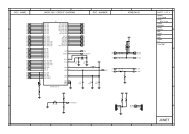
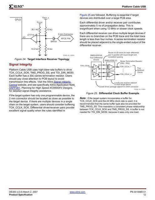
CPLD<br />
V CC33<br />
V REF_A<br />
Figure 25 are followed. Buffering is essential if target<br />
devices are distributed over a large PCB area.<br />
Each differential driver and/or receiver pair contributes<br />
approximately 5 ns of propagation delay. This is<br />
insignificant when using 12 MHz or slower clock speeds.<br />
I/O<br />
LT1719<br />
BAT54<br />
2 mm Connector<br />
XFCE PIN<br />
Each differential receiver can drive multiple target devices if<br />
there are no branches on the PCB trace and the total trace<br />
length is less than four inches. A series termination resistor<br />
should be placed adjacent to the single-ended output of the<br />
differential receiver.<br />
Figure 24: Target Interface Receiver Topology<br />
Signal Integrity<br />
DS300_23_120904<br />
<strong>Plat<strong>for</strong>m</strong> <strong>Cable</strong> <strong>USB</strong> uses high-slew-rate buffers to drive<br />
TCK_CCLK_SCK, TMS_PROG_SS, and TDI_DIN_MOSI.<br />
Each buffer has a 30Ω series termination resistor. Users<br />
should pay close attention to PCB layout to avoid<br />
transmission line effects. Visit the <strong>Xilinx</strong> Signal Integrity<br />
Central website, and see specifically <strong>Xilinx</strong> Application Note<br />
XAPP361, Planning <strong>for</strong> High Speed XC9500XV Designs,<br />
<strong>for</strong> detailed signal integrity assistance.<br />
If the target system has only one programmable device, the<br />
2 mm connector should be located as close as possible to<br />
the target device. If there are multiple devices in a single<br />
chain on the target system, users should consider buffering<br />
TCK_CCLK_SCK. Differential driver/receiver pairs provide<br />
excellent signal quality when the rules identified in<br />
TCK_CCLK<br />
Route A & B traces <strong>for</strong> each differential<br />
SN65LVDS105<br />
Four Differential<br />
pair in parallel with equal length and<br />
consistent spacing<br />
Drivers SN65LVDS2 (2)<br />
Series Termination Resistor<br />
1<br />
TCK_CCLK_1<br />
4 TCK_CCLK_4<br />
Locate one receiver adacent<br />
to each target device<br />
Locate driver package adjacent to 2mm connector<br />
Figure 25: Differential Clock Buffer Example<br />
Four<br />
Buffered<br />
Clocks<br />
DS300_24_110804<br />
Note: If the target system incorporates a buffer <strong>for</strong><br />
TCK_CCLK_SCK and the 24 MHz clock rate is used, it is<br />
recommended that the same buffer type also be provided <strong>for</strong><br />
TMS_PROG_SS. This maintains a consistent phase relationship<br />
between TCK_CCLK_SCK and TMS_PROG_SS. A buffer is not<br />
needed <strong>for</strong> TDI_DIN_MOSI, because it sees only one load.<br />
DS300 (v3.0) March 2, 2007 www.xilinx.com PN 0010989 01<br />
Product Specification 12