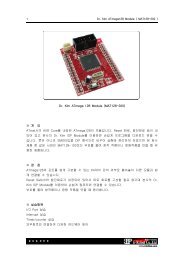
Platform Cable USB 2 JTAG (for Xilinx)
Platform Cable USB 2 JTAG (for Xilinx)
Platform Cable USB 2 JTAG (for Xilinx)

Create successful ePaper yourself
Turn your PDF publications into a flip-book with our unique Google optimized e-Paper software.
R<br />
<strong>Plat<strong>for</strong>m</strong> <strong>Cable</strong> <strong>USB</strong><br />
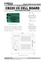
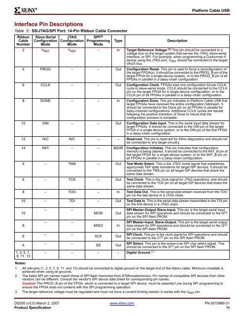
Interface Pin Descriptions<br />
Table 5: SS/<strong>JTAG</strong>/SPI Port: 14-Pin Ribbon <strong>Cable</strong> Connector<br />
Ribbon<br />
<strong>Cable</strong><br />
Number<br />
Slave-Serial<br />
Configuration<br />
Mode<br />
<strong>JTAG</strong><br />
Configuration<br />
Mode<br />
SPI (2)<br />
Programming<br />
Mode<br />
Type<br />
Description<br />
2 V REF V REF – In Target Reference Voltage. (3) This pin should be connected to a<br />
voltage bus on the target system that serves the <strong>JTAG</strong>, slave-serial<br />
interface. or SPI. For example, when programming a Coolrunner-II<br />
device using the <strong>JTAG</strong> port, V REF should be connected to the target<br />
VAUX bus.<br />
4 PROG – – Out Configuration Reset. This pin is used to <strong>for</strong>ce a reconfiguration of<br />
the target FPGA(s). It should be connected to the PROG_B pin of the<br />
target FPGA <strong>for</strong> a single-device system, or to the PROG_B pin of all<br />
FPGAs in parallel in a daisy-chain configuration.<br />
6 CCLK – – Out Configuration Clock. FPGAs load one configuration bit per CCLK<br />
cycle in slave-serial mode. CCLK should be connected to the CCLK<br />
pin on the target FPGA <strong>for</strong> a single-device configuration, or to the<br />
CCLK pin of all FPGAs in parallel in a daisy-chain configuration.<br />
8 DONE – – In Configuration Done. This pin indicates to <strong>Plat<strong>for</strong>m</strong> <strong>Cable</strong> <strong>USB</strong> that<br />
target FPGAs have received the entire configuration bitstream. It<br />
should be connected to the Done pin on all FPGAs in parallel <strong>for</strong><br />
daisy-chained configurations. Additional CCLK cycles are issued<br />
following the positive transition of Done to insure that the<br />
configuration process is complete.<br />
10 DIN – – Out Configuration Data Input. This is the serial input data stream <strong>for</strong><br />
target FPGAs. It should be connected to the DIN pin of the target<br />
FPGA in a single-device system, or to the DIN pin of the first FPGA<br />
in a daisy-chain configuration.<br />
12 N/C N/C – – Reserved. This pin is reserved <strong>for</strong> <strong>Xilinx</strong> diagnostics and should not<br />
be connected to any target circuitry.<br />
14 INIT – – BIDIR Configuration Initialize. This pin indicates that configuration<br />
memory is being cleared. It should be connected to the INIT_B pin of<br />
the target FPGA <strong>for</strong> a single-device system, or to the INIT_B pin on<br />
all FPGAs in parallel in a daisy-chain configuration.<br />
4 – TMS – Out Test Mode Select. This is the <strong>JTAG</strong> mode signal that establishes<br />
appropriate TAP state transitions <strong>for</strong> target ISP devices. It should be<br />
connected to the TMS pin on all target ISP devices that share the<br />
same data stream.<br />
6 – TCK – Out Test Clock. This is the clock signal <strong>for</strong> <strong>JTAG</strong> operations, and should<br />
be connected to the TCK pin on all target ISP devices that share the<br />
same data stream.<br />
8 – TDO – In Test Data Out. This is the serial data stream received from the TDO<br />
pin on the last device in a <strong>JTAG</strong> chain.<br />
10 – TDI – Out Test Data In. This is the serial data stream transmitted to the TDI pin<br />
on the first device in a <strong>JTAG</strong> chain.<br />
10<br />
8<br />
6<br />
4<br />
1, 3, 5, 7,<br />
9, 11, 13<br />
– –<br />
– –<br />
– –<br />
– –<br />
MOSI<br />
MISO<br />
SCK<br />
SS<br />
Out<br />
In<br />
Out<br />
Out<br />
– – – – Digital Ground. (1)<br />
SPI Master-Output Slave-Input. This pin is the target serial input<br />
data stream <strong>for</strong> SPI operations and should be connected to the D (2)<br />
pin on the SPI flash PROM.<br />
SPI Master-Input, Slave-Output. This pin is the target serial output<br />
data stream <strong>for</strong> SPI operations and should be connected to the Q (2)<br />
pin on the SPI flash PROM.<br />
SPI Clock. This pin is the clock signal <strong>for</strong> SPI operations and should<br />
be connected to the C (2) pin on the SPI flash PROM.<br />
SPI Select. This pin is the active-Low SPI chip select signal. This<br />
should be connected to the S (2) pin on the SPI flash PROM.<br />
Notes:<br />
1. All odd pins (1, 3, 5, 7, 9, 11, and 13) should be connected to digital ground on the target end of the ribbon cable. Minimum crosstalk is<br />
achieved when using all grounds.<br />
2. The listed SPI pin names match those of SPI flash memories from STMicroelectronics. Pin names of compatible SPI devices from other<br />
vendors can be different. Consult the vendor's SPI device data sheet <strong>for</strong> corresponding pin names.<br />
Caution! The PROG_B pin of the FPGA, which is connected to a target SPI device, must be asserted Low during SPI programming to<br />
ensure the FPGA does not contend with the SPI programming operation.<br />
3. The target reference voltage must be regulated and must not have a current-limiting resistor in series with the V REF pin.<br />
DS300 (v3.0) March 2, 2007 www.xilinx.com PN 0010989 01<br />
Product Specification 16