Platform Cable USB 2 JTAG (for Xilinx)
Platform Cable USB 2 JTAG (for Xilinx)
Platform Cable USB 2 JTAG (for Xilinx)

You also want an ePaper? Increase the reach of your titles
YUMPU automatically turns print PDFs into web optimized ePapers that Google loves.
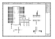
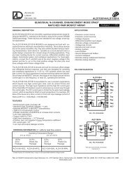
R<br />
<strong>Plat<strong>for</strong>m</strong> <strong>Cable</strong> <strong>USB</strong><br />
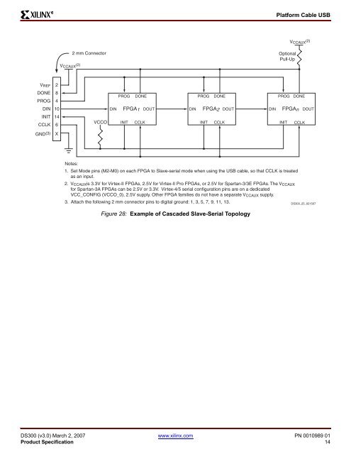
V CCAUX<br />
(2)<br />
V CCAUX<br />
(2)<br />
2 mm Connector<br />
Optional<br />
Pull-Up<br />
V REF 2<br />
DONE 8<br />
PROG 4<br />
DIN 10<br />
INIT<br />
CCLK<br />
14<br />
6<br />
GND (3) X<br />
VCCO<br />
DIN<br />
PROG DONE<br />
PROG DONE<br />
PROG DONE<br />
FPGA 1 DOUT<br />
DIN FPGA 2 DOUT<br />
DIN FPGA n<br />
INIT CCLK<br />
INIT CCLK<br />
INIT CCLK<br />
DOUT<br />
Notes:<br />
1. Set Mode pins (M2-M0) on each FPGA to Slave-serial mode when using the <strong>USB</strong> cable, so that CCLK is treated<br />
as an input.<br />
2. V CCAUX is 3.3V <strong>for</strong> Virtex-II FPGAs, 2.5V <strong>for</strong> Virtex-II Pro FPGAs, or 2.5V <strong>for</strong> Spartan-3/3E FPGAs. The V CCAUX<br />
<strong>for</strong> Spartan-3A FPGAs can be 2.5V or 3.3V. Virtex-4/5 serial configuration pins are on a dedicated<br />
VCC_CONFIG (VCCO_0), 2.5V supply. Other FPGA families do not have a separate V CCAUX supply.<br />
3. Attach the following 2 mm connector pins to digital ground: 1, 3, 5, 7, 9, 11, 13.<br />
Figure 28: Example of Cascaded Slave-Serial Topology<br />
DS300_25_021507<br />
DS300 (v3.0) March 2, 2007 www.xilinx.com PN 0010989 01<br />
Product Specification 14