Platform Cable USB 2 JTAG (for Xilinx)
Platform Cable USB 2 JTAG (for Xilinx)
Platform Cable USB 2 JTAG (for Xilinx)

Create successful ePaper yourself
Turn your PDF publications into a flip-book with our unique Google optimized e-Paper software.
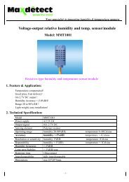
R<br />
<strong>Plat<strong>for</strong>m</strong> <strong>Cable</strong> <strong>USB</strong><br />
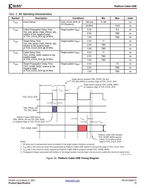
Table 8: AC Operating Characteristics<br />
Symbol Description Conditions Min Max Units<br />
T CLK Clock Period TCK_CCLK_SCK_S<br />
CK frequency:<br />
T CPD<br />
T TSU<br />
T CSU<br />
T TPD<br />
<strong>Cable</strong> Propagation Delay Time<br />
TDI_DIN_MOSI (TMS_PROG_SS)<br />
relative to the negative edge<br />
of TCK_CCLK_SCK @ 24 MHz<br />
Target Setup Time<br />
TDI_DIN_MOSI (TMS_PROG_SS)<br />
relative to the positive edge<br />
of TCK_CCLK_SCK @ 24 MHz<br />
<strong>Cable</strong> Setup Time<br />
TDO_DONE_MISO relative to the<br />
positive edge<br />
of TCK_CCLK_SCK @ 24 MHz<br />
Target Propagation Delay Time<br />
TDO_DONE_MISO relative to the<br />
negative edge<br />
of TCK_CCLK_SCK @ 24 MHz<br />
750 kHz 41.66 ns<br />
24 MHz 1333 ns<br />
Target system V REF : 3.3V 9.2 ns<br />
2.5V TBD ns<br />
1.8V TBD ns<br />
Target system V REF : 3.3V 11 ns<br />
2.5V TBD ns<br />
1.8V TBD ns<br />
Target system V REF : 3.3V 11 ns<br />
2.5V TBD ns<br />
1.8V TBD ns<br />
Target system V REF : 3.3V 10 ns<br />
2.5V TBD ns<br />
1.8V TBD ns<br />
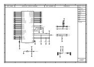
T CLK<br />
Target device samples TMS_PROG_SS and<br />
TDI_DIN_MOSI on positive edge of TCK_CCLK_SCK<br />
Target device asserts TDO_DONE_MISO<br />
on negative edge of TCK_CCLK_SCK<br />
T TSU<br />
TCK_CCLK_SCK<br />
T CPD<br />
T TPD<br />
DS300_28_021707<br />
TMS_PROG_SS/<br />
TDI_DIN_MOSI<br />
<strong>Plat<strong>for</strong>m</strong> <strong>Cable</strong> <strong>USB</strong> asserts<br />
TMS_PROG_SS and TDI_DIN_MOSI<br />
on negative edge of TCK_CCLK_SCK<br />
T CSU<br />
TDO_DONE_MISO<br />
<strong>Plat<strong>for</strong>m</strong> cable <strong>USB</strong> samples<br />
TDO_DONE_MISO approximately<br />
15 ns after positive<br />
Notes:<br />
edge of TCK_CCLK_SCK<br />
1. All times are in nanoseconds and are relative to the target system interface connector.<br />
2. T TSU Min is the minimum setup time guaranteed by <strong>Plat<strong>for</strong>m</strong> <strong>Cable</strong> <strong>USB</strong> relative to the positive edge of TCK_CCLK_SCK.<br />
3. T CSU Min is the minimum setup required by <strong>Plat<strong>for</strong>m</strong> <strong>Cable</strong> <strong>USB</strong> to properly sample TDO_DONE_MISO.<br />
4. Propagation delays associated with buffers on the target system must be taken into account to satisfy the minimum setup times.<br />
Figure 30: <strong>Plat<strong>for</strong>m</strong> <strong>Cable</strong> <strong>USB</strong> Timing Diagram<br />
DS300 (v3.0) March 2, 2007 www.xilinx.com PN 0010989 01<br />
Product Specification 18