LinkSwitch-HP Family - Codico
LinkSwitch-HP Family - Codico
LinkSwitch-HP Family - Codico

You also want an ePaper? Increase the reach of your titles
YUMPU automatically turns print PDFs into web optimized ePapers that Google loves.
<strong>LinkSwitch</strong>-<strong>HP</strong><br />
Layout Considerations for eSIP-7C Package<br />
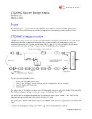
Figure 12 is the layout for a 30 W adapter shown in the schematic<br />
Figure 11. An eSIP-7C package is used as indicated by the<br />
suffix in LNK6766E which allows the use of a stand-up heat<br />
sink. The mounting pin for the heat sink should be electrically<br />
isolated. It can be seen that the primary return trace wraps<br />
around the <strong>LinkSwitch</strong>-<strong>HP</strong> device which acts as a shield around<br />
the critical external control related components of <strong>LinkSwitch</strong>-<strong>HP</strong>.<br />
These components include R7, R8, R19, R20 and C5, C8, C20.<br />
Of particular importance is placing the bypass capacitor C5 and<br />
COMPENSATION pin noise filter capacitor C8 as close as<br />
possible to SOURCE pin with very short trace lengths to<br />
COMPENSATION and BYPASS pins as done in the layout<br />
above. The ground trace wrap, tight layout and single point<br />
grounding to SOURCE pin of these components avoids having<br />
noise related issues during peak loads or during line transient<br />
such as surge or ESD events.<br />
Another consideration for ESD and line surge is the primaryside<br />
termination of the Y capacitor. The Y capacitor C18 should<br />
be tied to the positive terminal of the bulk capacitor C2 in order<br />
to route the potential of high currents away from the more<br />
sensitive primary return traces.<br />
Because of the tight layout common to adapter applications,<br />
this design uses triple insulated wire and flying leads for output<br />
winding termination to avoid secondary arcing to core during<br />
ESD events.<br />
The trace connecting the drain to transformer should be very<br />
short and the primary clamp circuitry should be grouped<br />
together and away from the more sensitive components. The<br />
bias winding return and return of bias capacitor C6 should be<br />
routed separately to the negative terminal of the input capacitor<br />
C2 away from SOURCE pin.<br />
The secondary rectifying loop that includes the secondary<br />
winding, the output diode D8, and the first output capacitor C13<br />
should be as tight as possible to minimize adding series<br />
inductance which can reduce high load efficiency and degrade<br />
the quality of regulation.<br />
Figure 12. Layout for 30 W Adapter Using a eSIP-7C Package.<br />
10<br />
Rev. A 07/12<br />
www.powerint.com