LinkSwitch-HP Family - Codico
LinkSwitch-HP Family - Codico
LinkSwitch-HP Family - Codico

You also want an ePaper? Increase the reach of your titles
YUMPU automatically turns print PDFs into web optimized ePapers that Google loves.
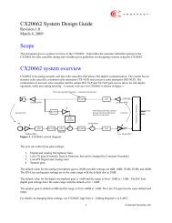
<strong>LinkSwitch</strong>-<strong>HP</strong><br />
Absolute Maximum Ratings (3)<br />
DRAIN Pin Voltage....................................-0.3 V to 725 V (677x)<br />
DRAIN Pin Voltage...........................-0.3 V to 650 V (666x/676x)<br />
DRAIN Pin Peak Current: ……………………........... 1.6 x I LIMIT(TYP)<br />
(1)<br />
BYPASS Pin Voltage .............................................. -0.3 V to 9 V<br />
BYPASS Pin Current ..................................................... 100 mA<br />
FEEDBACK Pin Voltage ........................................-0.3 V to 9 V (2)<br />
COMPENSATION Pin Voltage ................................ -0.3 V to 9 V<br />
PROGRAM/DELAY Pin Voltage............................... -0.3 V to 9 V<br />
Storage Temperature....................................... -65 °C to 150 °C<br />
Operating Junction Temperature ................... -40 °C to 150 °C (4)<br />
Notes:<br />
1. Peak DRAIN current is allowed while the DRAIN voltage is<br />
simultaneously less than 400 V.<br />
2. -1 V for current pulses ≤5 mA out of the pin and a duration<br />
of ≤500 ns.<br />
3. Maximum ratings specified may be applied one at a time<br />
without causing permanent damage to the product.<br />
Exposure to Absolute Maximum Rating conditions for<br />
extended periods of time may affect product reliability.<br />
4. Normally limited by internal circuitry.<br />
Thermal Resistance<br />
Thermal Resistance: E Package<br />
Notes:<br />
(q JA<br />
)........................................... 105 °C/W (1)<br />
(q JC<br />
)............................................... 2 °C/W (2)<br />
V Package<br />
(q JA<br />
) .......................... .74 °C/W (3) , 63 °C/W (4)<br />
(q JC<br />
)............................................... 2 °C/W (2)<br />
1. Free standing with no heat sink.<br />
2. Measured at the back surface of tab.<br />
3. Soldered to typical application PCB with a heat sinking area<br />
of 0.36 sq. in. (232 mm 2 ), 2 oz. (610 g/m 2 ) copper clad.<br />
4. Soldered to typical application PCB with a heat sinking area<br />
of 1 sq. in. (645 mm 2 ), 2 oz. (610 g/m 2 ) copper clad.<br />
Parameter<br />
Symbol<br />
Conditions<br />
SOURCE = 0 V; T J<br />
= -40 to 125 °C<br />
(Unless Otherwise Specified)<br />
Min Typ Max Units<br />
Control Functions<br />
Switching Frequency f OSC<br />
Average value, T J<br />
= +25 °C, 120 132 136 kHz<br />
Switching Frequency<br />
Temperature Variation<br />
Frequency Jitter<br />
Deviation<br />
Frequency Jitter<br />
Modulation Rate<br />
Δf OSC<br />
0 °C ≤ T J<br />
≤ +100 °C, See Note A ±10 %<br />
Δf f OSC<br />
= 128 kHz ±5 kHz<br />
f M<br />
250 Hz<br />
Maximum Duty Cycle DC MAX<br />
VFB < V FB(REF)<br />
Maximum Duty Cycle<br />
Temperature Variation<br />
∆DC MAX<br />
V FB(REF)<br />
= 2 V<br />
Minimum Peak<br />
Current to Set<br />
Current Limit Ratio<br />
Multi-Cycle<br />
Modulation Switching<br />
Frequency<br />
Multi-Cycle<br />
Modulation Max<br />
Off-Time<br />
T J<br />
= +25 °C 62 64 66 %<br />
See Note A<br />
0 °C ≤ T J<br />
≤ +100 °C<br />
+2% %<br />
k PS<br />
T J<br />
= +25 °C<br />
di/dt (KPS)<br />
= di/dt (ILIMIT)<br />
23 25 %<br />
f MCM<br />
T J<br />
= +25 °C 25 32 kHz<br />
T MCM(OFF)<br />
T J<br />
= +25 °C<br />
LNK666x 0.5<br />
LNK67xx 4<br />
Soft-Start Time t SOFT<br />
T J<br />
= +25 °C 15 ms<br />
ms<br />
Auto-Restart Shut-<br />
Down Default Delay<br />
t SD(AR)<br />
T J<br />
= +25 °C 35 ms<br />
Auto-Restart<br />
t AR(ON) T J<br />
= +25 °C, t SOFT<br />
+ t SD(AR)<br />
50<br />
T AR(OFF)1 First switch off-period 150<br />
T AR(OFF)2<br />
Subsequent switch off-periods 1500<br />
ms<br />
12<br />
Rev. A 07/12<br />
www.powerint.com