LinkSwitch-HP Family - Codico
LinkSwitch-HP Family - Codico
LinkSwitch-HP Family - Codico

You also want an ePaper? Increase the reach of your titles
YUMPU automatically turns print PDFs into web optimized ePapers that Google loves.
<strong>LinkSwitch</strong>-<strong>HP</strong><br />
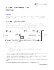
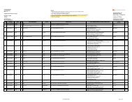
Applications Example<br />
30 W, 12 V Universal Adapter<br />
The circuit shown in Figure 11 is a high efficiency universal input<br />
30 W, 12 V output adapter using the LNK6766E.<br />
The supply uses primary winding coupled sensing for the<br />
following features: output regulation, line undervoltage lockout,<br />
input and output OVP. With primary winding sense there is no<br />
need for an external secondary referenced error amplifier such<br />
as a TL431 and optocoupler. The winding sense of bus voltage<br />
also eliminates the need for direct input voltage sensing which<br />
requires more components and is more dissipative than winding<br />
sense method.<br />
Output regulation is ±5%, active-on efficiency is 86% and<br />
no-load input power is less than 30 mW.<br />
The rectified and filtered input voltage is applied to the primary<br />
winding of T1. The other side of the primary is driven by the<br />
integrated power MOSFET in U3. Diode D1, C3, R2, R3 and<br />
VR1 comprise the clamp circuit, limiting the leakage inductance<br />
turn-off voltage spike to safe value. Zener diode VR1 also helps<br />
to reduce input power consumption during no-load conditions.<br />
Start-up of the power supply is initiated by sensing the forward<br />
negative pulse current from feedback winding through R19 into<br />
the FEEDBACK pin. This sensing is accomplished by periodically<br />
turning on the power MOSFET to sense input voltage condition<br />
with very short low frequency sampling pulses. During the<br />
forward pulse sampling time the FEEDBACK pin is held to zero<br />
volts by an internal clamp. When negative forward pulse<br />
current exceeds 250 mA, <strong>LinkSwitch</strong>-<strong>HP</strong> for two consecutive<br />
switching cycles will initiate start-up with a soft-start sequence<br />
that reduces component stress and allows the output to rise in<br />
a smooth monotonic manner. The desired input voltage for<br />
start-up is determined by the turns ratio of primary winding to<br />
feedback winding and the value of R19.<br />
Regulation is accomplished by sampling the feedback winding<br />
during flyback period through the resistor divider R19 and R20<br />
through FEEDBACK pin. This sampled voltage is compared to<br />
an internal error amplifier threshold of 2 V. The value of R19 is<br />
already determined by the line undervoltage function so the<br />
output regulation point is determined by setting the proper<br />
value for R20.<br />
The loop compensation is provided by the network from<br />
COMPENSATION pin to ground. In the case above, a low<br />
frequency to mid frequency gain of 20 dB for the error amplifier<br />
is established by R7 and C7. Capacitor C8 functions essentially<br />
as a noise filter and is typically 100 pF. There is also an internal<br />
16 kHz filter within the device. It is advised to limit R7 to no<br />
greater than 260 kW to avoid stability and noise sensitivity.<br />
L4<br />
10 mH<br />
BR1<br />
2KBP06M<br />
600 V<br />
C14<br />
150 nF<br />
275 VAC<br />
C2<br />
68 µF<br />
400 V<br />
R3<br />
VR1<br />
BZY97C150<br />
150 V<br />
D1<br />
DL4937<br />
C18<br />
1 nF<br />
250 VAC<br />
3 kΩ C12 C21<br />
R28<br />
C3<br />
680 µF 470 µF<br />
27 kΩ<br />
10 nF<br />
25 V 25 V<br />
630 V<br />
R2<br />
20 Ω<br />
1%<br />
9<br />
T1<br />
RM8<br />
FL1<br />
FL2<br />
7<br />
6 8<br />
R13<br />
C13 10 Ω<br />
470 pF 1%<br />
200 V 1/8 W<br />
D8<br />
V12P10-M3/86A<br />
D2<br />
BAV21WS- C6<br />
7-F 22 µF<br />
16 V<br />
R19<br />
51.1 kΩ<br />
1%<br />
R9<br />
4.32 kΩ<br />
1%<br />
1/8 W<br />
L5<br />
100 µH<br />
C22<br />
100 nF<br />
50 V<br />
12 V, 2.5 A<br />
J3<br />
RTN<br />
J4<br />
F1<br />
2 A<br />
R29 R30<br />
3.3 MΩ 3.3 MΩ<br />
J1<br />
90 - 265<br />
VAC<br />
J2<br />
<strong>LinkSwitch</strong>-<strong>HP</strong><br />
U3<br />
LNK6766E<br />
C20<br />
4.7 nF<br />
50 V<br />
R8<br />
23.2 kΩ<br />
1%<br />
1/8 W<br />
D<br />
S<br />
PD<br />
BP<br />
CONTROL<br />
CP<br />
FB<br />
R7<br />
120 kΩ<br />
1/8 W<br />
C7<br />
100 nF<br />
25 V<br />
C8<br />
100 pF<br />
50 V<br />
R20<br />
12.4 kΩ<br />
1%<br />
1/8 W<br />
C5<br />
470 nF<br />
50 V<br />
PI-6844-072312<br />
Figure 11. Schematic of a Universal Input 30 W, 12 V, 2.5 A Adapter.<br />
8<br />
Rev. A 07/12<br />
www.powerint.com