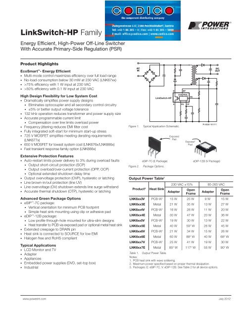
LinkSwitch-HP Family - Codico
LinkSwitch-HP Family - Codico
LinkSwitch-HP Family - Codico

You also want an ePaper? Increase the reach of your titles
YUMPU automatically turns print PDFs into web optimized ePapers that Google loves.
<strong>LinkSwitch</strong>-<strong>HP</strong> <strong>Family</strong><br />
Energy Efficient, High-Power Off-Line Switcher<br />
With Accurate Primary-Side Regulation (PSR)<br />
Product Highlights<br />
EcoSmart - Energy Efficient<br />
• Multi-mode control maximizes efficiency over full load range<br />
• No-load consumption below 30 mW at 230 VAC (LNK67xx)<br />
• >75% efficiency with 1 W input at 230 VAC<br />
• >50% efficiency with 0.1 W input at 230 VAC<br />
AC<br />
IN<br />
D<br />
BP<br />
DC<br />
OUT<br />
High Design Flexibility for Low System Cost<br />
• Dramatically simplifies power supply designs<br />
• Eliminates optocoupler and all secondary control circuitry<br />
• ±5% or better output voltage tolerance<br />
• 132 kHz operation reduces transformer and power supply size<br />
• Accurate programmable current limit<br />
• Compensation over line limits overload power<br />
• Frequency jittering reduces EMI filter cost<br />
• Fully integrated soft-start for minimum start-up stress<br />
• 725 V MOSFET simplifies meeting derating requirements<br />
(LNK677x)<br />
• 650 V MOSFET for lowest system cost (LNK676x/LNK666x)<br />
• Fast transient response family option (LNK666x)<br />
Figure 1.<br />
<strong>LinkSwitch</strong>-<strong>HP</strong><br />
Typical Application Schematic.<br />
S<br />
Exposed<br />
Pad<br />
CONTROL<br />
PD<br />
CP<br />
FB<br />
Exposed<br />
Pad<br />
PI-6530-101711<br />
Extensive Protection Features<br />
• Auto-restart limits power delivery to 3% during overload faults<br />
• Output short-circuit protection (SCP)<br />
• Output overload/over-current protection (OPP, OCP)<br />
• Optional extended shutdown delay time<br />
• Output overvoltage protection (OVP), hysteretic or latching<br />
• Line brown-in/out protection (line UV)<br />
• Line overvoltage (OV) shutdown extends line surge withstand<br />
• Accurate thermal shutdown (OTP), hysteretic or latching<br />
Advanced Green Package Options<br />
• eSIP -7C package:<br />
• Vertical orientation for minimum PCB footprint<br />
• Simple heat sink mounting using clip or adhesive pad<br />
• eDIP -12B package:<br />
• Low profile through-hole mounted for ultra-slim designs<br />
• Heat transfer to PCB via exposed pad or optional metal heat sink<br />
• Extended creepage to DRAIN pin<br />
• Heat sink is connected to SOURCE for low EMI<br />
• Halogen free and RoHS compliant<br />
Typical Applications<br />
• LCD Monitor and TV<br />
• Adapter<br />
• Appliances<br />
• Embedded power supplies (DVD, set-top box)<br />
• Industrial<br />
Figure 2.<br />
Output Power Table 1<br />
Product 3<br />
eSIP-7C (E Package)<br />
Package Options.<br />
Heat Sink<br />
230 VAC ±15% 85-265 VAC<br />
Adapter<br />
Open<br />
Frame<br />
eDIP-12B (V Package)<br />
Adapter<br />
Open<br />
Frame<br />
LNK6xx3V PCB-W 1 15 W 25 W 9 W 15 W<br />
LNK6xx3E Metal 21 W 35 W 13 W 27 W<br />
LNK6xx4V PCB-W 1 16 W 28 W 11 W 20 W<br />
LNK6xx4E Metal 30 W 47 W 20 W 36 W<br />
LNK6xx5V PCB-W 1 19 W 30 W 13 W 22 W<br />
LNK6xx5E Metal 40 W 59 2 W 26 W 45 W<br />
LNK6xx6V PCB-W 1 21 W 34 W 15 W 26 W<br />
LNK6xx6E Metal 60 W 88 2 W 40 W 68 2 W<br />
LNK6xx7V PCB-W 1 25 W 41 W 19 W 30 W<br />
LNK6xx7E Metal 85 2 W 117 2 W 55 W 90 2 W<br />
Table 1. Output Power Table.<br />
Notes:<br />
1. PCB heat sink with wave soldering.<br />
2. Maximum power specified based on proper thermal dissipation.<br />
3. Packages: E: eSIP-7C, V: eDIP-12B. See Table 2 for all device options.<br />
www.powerint.com July 2012
<strong>LinkSwitch</strong>-<strong>HP</strong><br />
BYPASS<br />
(BP)<br />
LATCH/HYSTERETIC<br />
5.75 V<br />
REGULATOR<br />
DRAIN<br />
(D)<br />
THERMAL<br />
SHUTDOWN<br />
FAULT FILTER<br />
+<br />
COMPENSATION<br />
(CP)<br />
BYPASS<br />
PROGRAM<br />
MULTI-CYCLE<br />
MODE CONTROL<br />
MCM<br />
5.75 V<br />
4.9 V<br />
-<br />
2 V<br />
REFERENCE<br />
VOLTAGE<br />
FEEDBACK<br />
(FB)<br />
+<br />
SOFT-<br />
START<br />
S/H<br />
OV<br />
AUTO-<br />
RESTART<br />
OUTPUT<br />
OVERVOLTAGE<br />
AUTO-RESTART<br />
HIGH GAIN<br />
TRANS-<br />
CONDUCTANCE<br />
AMPLIFIER<br />
+<br />
AMP<br />
ERROR<br />
VOLTAGE<br />
GATE<br />
DRIVER<br />
PROGRAM/<br />
DELAY<br />
(PD)<br />
LINE<br />
COMP<br />
LINE<br />
COMPENSATION<br />
LINE OVERVOLTAGE/<br />
UNDERVOLTAGE<br />
DETECTION<br />
LUV<br />
LOV<br />
CUSTOM<br />
SHUTDOWN<br />
DELAY<br />
CLOCK<br />
OSC<br />
DC MAX<br />
OSCILLATOR<br />
PROGRAM<br />
I LIM<br />
40% ~ 100%<br />
CURRENT<br />
LIMIT<br />
SETTING<br />
S<br />
R<br />
Q<br />
Q<br />
LEB<br />
CURRENT LIMIT<br />
COMPARATOR<br />
PI-6565-072012<br />
+<br />
SOURCE<br />
(S)<br />
Figure 3.<br />
Block Diagram.<br />
Part Number BV DSS<br />
1<br />
T MCM(OFF)<br />
2<br />
Packages<br />
LNK6663E/V 650 V 0.5 ms eSIP-7C (E), eDIP-12B (V)<br />
LNK6664E/V 650 V 0.5 ms eSIP-7C (E), eDIP-12B (V)<br />
LNK6665E/V 650 V 0.5 ms eSIP-7C (E), eDIP-12B (V)<br />
LNK6666E/V 650 V 0.5 ms eSIP-7C (E), eDIP-12B (V)<br />
LNK6667E/V 650 V 0.5 ms eSIP-7C (E), eDIP-12B (V)<br />
LNK6763E/V 650 V 4.0 ms eSIP-7C (E), eDIP-12B (V)<br />
LNK6764E/V 650 V 4.0 ms eSIP-7C (E), eDIP-12B (V)<br />
LNK6765E/V 650 V 4.0 ms eSIP-7C (E), eDIP-12B (V)<br />
LNK6766E/V 650 V 4.0 ms eSIP-7C (E), eDIP-12B (V)<br />
LNK6767E/V 650 V 4.0 ms eSIP-7C (E), eDIP-12B (V)<br />
LNK6773E/V 725 V 4.0 ms eSIP-7C (E), eDIP-12B (V)<br />
LNK6774E/V 725 V 4.0 ms eSIP-7C (E), eDIP-12B (V)<br />
LNK6775E/V 725 V 4.0 ms eSIP-7C (E), eDIP-12B (V)<br />
LNK6776E/V 725 V 4.0 ms eSIP-7C (E), eDIP-12B (V)<br />
LNK6777E/V 725 V 4.0 ms eSIP-7C (E), eDIP-12B (V)<br />
Table 2. Device Part Numbers and Options.<br />
Notes:<br />
1. Minimum breakdown voltage at T J<br />
= +25 °C.<br />
2. T MCM(OFF)<br />
= 0.5 ms for fastest transient response, T MCM(OFF)<br />
= 4 ms for
<strong>LinkSwitch</strong>-<strong>HP</strong><br />
Pin Functional Description<br />
BYPASS (BP) Pin:<br />
An external bypass capacitor is connected to this pin for the<br />
internally generated 5.75 V supply. Based on the connected<br />
capacitance determined at start-up, it will provide either<br />
auto-restart or latching shutdown option dependant on the fault<br />
condition. Please see Table 2.<br />
COMPENSATION (CP) Pin:<br />
This pin is the output of transconductance amplifier. An RC<br />
compensation network on this pin provides control loop<br />
compensation.<br />
DRAIN (D) Pin:<br />
This pin is the high-voltage power MOSFET drain connection. It<br />
also provides internal operating current for start-up until output<br />
is in regulation.<br />
FEEDBACK (FB) Pin:<br />
The FEEDBACK pin is used to sense output and input voltage<br />
by sensing the auxiliary winding voltage. During MOSFET<br />
on-time, the current out of the FEEDBACK pin is sensed to<br />
detect the line voltage. During the secondary rectifier<br />
conduction time, the feedback voltage is proportional to the<br />
output voltage via the turns ratio between the bias and<br />
secondary windings.<br />
PROGRAM (PD) Pin:<br />
This MULTI-FUNCTIONAL pin sets device current limit and<br />
optional shutdown delay time extension. During start-up, the<br />
internal circuit decodes the current limit based on resistor<br />
loaded on the PROGRAM pin. Please see Table 3. It can also<br />
be used for optionally extending shutdown delay time by<br />
changing the capacitance on the pin. See Figure 6.<br />
SOURCE (S) Pin:<br />
This pin is the power MOSFET source connection. It is also the<br />
ground reference for the BYPASS, FEEDBACK, PROGRAM and<br />
COMPENSATION pins.<br />
E Package<br />
(eSIP-7C)<br />
1 2 3 4 5<br />
P F C B S<br />
D B P P<br />
7<br />
D<br />
Exposed Pad<br />
(Hidden)<br />
Internally<br />
Connected to<br />
SOURCE Pin<br />
S 12<br />
S 11<br />
S 10<br />
S 9<br />
S 8<br />
S 7<br />
Exposed Pad Internally<br />
Connected to SOURCE Pin<br />
V Package<br />
(eDIP-12)<br />
1 PD<br />
2 FB<br />
3 CP<br />
4 BP<br />
6 D<br />
PI-6831-062212<br />
Functional Description<br />
A <strong>LinkSwitch</strong>-<strong>HP</strong> device monolithically integrates a controller<br />
and high-voltage power MOSFET into one package. It has a<br />
newly developed analogue control scheme, which enables<br />
continuous conduction mode (CCM), primary side regulated<br />
(PSR) power supplies up to 90 W without the efficiency<br />
limitation of DCM or audible noise. It uses an enhanced peak<br />
current mode PWM control scheme with multi-mode operation.<br />
The multi-mode control engine uses the error amplifier output<br />
signal voltage at the COMPENSATION pin to set the operating<br />
peak current and switching frequency to maintain the output<br />
voltage in regulation as shown in Figure 5. For COMPENSATION<br />
pin voltages lower than V C(MCM)<br />
(typ. 1.25 V) the device enters<br />
multi-cycle modulation (MCM) with a fixed peak current of 25%<br />
of the programmed current limit. Several innovative improvements<br />
have been added to the peak current mode control to allow<br />
primary side regulated CCM operation with no instability. The<br />
device meets less than 30 mW input power with no-load at<br />
high-line (LNK67xx families).<br />
It also offers extensive built-in features:<br />
• External current limit selection<br />
• Optional programmable shutdown delay time extension<br />
• Optional remote On/Off<br />
• Optional fast AC reset<br />
• Primary-side sensed output overvoltage protection (OVP)<br />
• Lost regulation protection during output overload or<br />
short-circuit (auto-restart)<br />
• Internal current limit over line compensation for constant<br />
overload power over line<br />
• High-voltage bus overvoltage sense (line OV) for extended line<br />
surge withstand<br />
• High-voltage bus undervoltage sense (line UV) for brown-in/<br />
out protection<br />
• Accurate over-temperature protection (OTP)<br />
• Output OVP/OCP/OTP shutdown type selection (hysteretic/<br />
latching)<br />
• Optional external latching shutdown input (current threshold)<br />
• Cycle-by-cycle current limit control<br />
Regulator/Shunt Voltage Clamp<br />
The internal 5.75 V regulator charges the bypass capacitor<br />
connected to the BYPASS pin to 5.75 V by drawing a current<br />
from DRAIN whenever the power MOSFET is off. When the<br />
power MOSFET is on, the device operates from the energy<br />
stored in the bypass capacitor. In addition, there is a shunt<br />
regulator clamping the bypass at 6.4 V when supply current is<br />
provided by a bias winding through an external resistor. This<br />
makes the device insensitive to bias winding voltage variations.<br />
Auto-Restart<br />
In the event of an open-loop fault (open feedback resistor or<br />
broken path to feedback winding), output short-circuit or<br />
overload condition, the device enters into auto-restart mode.<br />
Auto-restart minimizes the power dissipation under fault<br />
conditions, the device will turn on and off at duty cycle of<br />
Figure 4.<br />
Pin Configuration.<br />
www.powerint.com<br />
3<br />
Rev. A 07/12
<strong>LinkSwitch</strong>-<strong>HP</strong><br />
Frequency (kHz)<br />
Normalized Peak Current<br />
132<br />
f SW(LF)<br />
30<br />
100%<br />
50%<br />
25%<br />
V V C(MIN) C(MCM)<br />
V C(MAX)<br />
Compensation<br />
Voltage (∝ P OUT<br />
)<br />
Compensation<br />
Voltage (∝ P OUT<br />
)<br />
voltage is sampled after the turn-off of the internal switch to<br />
compensate for diode conduction time differences. Sampling<br />
time increases monotonically from 1.2 ms at no or light load to<br />
2.5 ms at full load. Sampled voltage is held until the next clock<br />
cycle. The output of S/H is fed to the error amplifier, once in<br />
regulation the sampled voltage is 2 V.<br />
BYPASS (BP) Programming<br />
This feature selects either hysteretic or latching OVP/OCP and<br />
OTP protection based on capacitor loading on the BYPASS pin.<br />
The shutdown type is determined at the device power-up as<br />
shown in Table 2.<br />
C BP<br />
0.47 mF 4.7 mF 47 mF<br />
OVP Latching Auto-Restart Latching<br />
Lost Regulation (SC,<br />
OC, Open-Loop<br />
Auto-Restart Auto-Restart Latching<br />
OTP Latching Hysteretic Latching<br />
Figure 5.<br />
PI-6722-032012<br />
Compensation Pin Characteristics (Multi-Mode Operation).<br />
typically 3% as long as the fault condition persists. In autorestart<br />
switching is disabled for t AR(OFF)1<br />
(typ. 1500 ms) when the<br />
FEEDBACK pin voltage has dropped below the auto-restart<br />
threshold V FB(AR)<br />
for the shutdown default delay time t AR(ON)<br />
(typ.<br />
35 ms). After this period switching is enabled again with the<br />
device entering soft-start (typ. 15 ms). For the first auto-restart<br />
off-period switching is disabled for a reduced time t AR(OFF)2<br />
(typ.<br />
150 ms) to reduce the power supply restart time during line<br />
cycling. Optionally the default shutdown delay time can be<br />
extended by adding a capacitor to the PROGRAM pin.<br />
Hysteretic Thermal Shutdown<br />
The thermal shutdown circuitry senses the controller die<br />
temperature. The threshold is set at 142 °C with a 75 °C<br />
hysteresis (both typical). Once the device temperature rises<br />
above 142 °C, the power MOSFET is disabled and remains<br />
disabled until the die temperature falls by 75 °C, at which point<br />
the device is re-enabled. The large hysteresis maintain the<br />
average temperature below the temperature rating of low cost<br />
CEM type PCB material in most cases.<br />
Safe Operating Area (SOA) Protection<br />
The device features a safe operating area (SOA) protection<br />
mode which disables MOSFET switching for 4 consecutive<br />
cycles in the event the peak switching current reaches the<br />
current limit in less than time t ON(SOA)<br />
. This prevents excessive<br />
drain currents during start-up and output short-circuit<br />
conditions by providing additional time for the primary<br />
inductance to reset. The SOA protection is disabled when the<br />
output voltage is within 10% of regulation voltage.<br />
Sample and Hold (S/H)<br />
The sample and hold block senses the output voltage at auxiliary<br />
winding during secondary rectifier on-time. The FEEDBACK pin<br />
Table 2.<br />
Current Limit Setting<br />
During power-up the cycle-by-cycle current limit is determined<br />
by measuring the resistor value connected to the PROGRAM<br />
pin by the measurement is performed by applying 1.25 V (see<br />
Figure 8). The current limit can be set between 40% to 100% in<br />
steps of 10% as shown in Table 3. After the current limit is set<br />
the PROGRAM pin voltage is reduced to ~0 in order to minimize<br />
power dissipation.<br />
Table 3.<br />
Shutdown Type vs. Value of BYPASS Pin Capacitance.<br />
I PD<br />
R PD<br />
I LIMIT(NORM)<br />
I PD<br />
R PD<br />
I LIMIT(NORM)<br />
mA kW % mA kW %<br />
10 124 100 54 23.2 60<br />
16 78.7 90 83 15.0 50<br />
24 52.3 80 125 10.0 40<br />
36 34.8 70<br />
Current Limit Selection vs. Program Pin Resistor Value.<br />
Programmable Shutdown Delay<br />
The default auto-restart shutdown delay time t SD(AR)<br />
(typ. 35 ms)<br />
can optionally be extended by connecting a capacitor to the<br />
PROGRAM pin. Once a lost regulation fault is detected the<br />
PROGRAM pin voltage is cycled 128 times between V PD(DL)<br />
(typ.<br />
0.5 V) and V PD(DU)<br />
(typ. 1.2 V) as shown in Figure 8. Figure 6<br />
depicts the relationship between extended shutdown delay<br />
time, added PROGRAM pin capacitor and current limit<br />
programming resistor.<br />
Remote On/Off and Fast AC Reset<br />
The PROGRAM pin can be used to turn on/off the device<br />
remotely. If the voltage on the pin is set to 1.3 V externally, the<br />
device stops switching. After releasing the PROGRAM pin the<br />
PROGRAM pin device commences switching when the voltage<br />
drops below 0.55 V.<br />
4<br />
Rev. A 07/12<br />
www.powerint.com
<strong>LinkSwitch</strong>-<strong>HP</strong><br />
Auto-Restart On-Time Extension (ms)<br />
500<br />
450<br />
400<br />
350<br />
300<br />
250<br />
200<br />
150<br />
100<br />
50<br />
PD Pin Resistor Value<br />
124 kΩ<br />
78.7 kΩ<br />
52.3 kΩ<br />
34.8 kΩ<br />
23.2 kΩ<br />
15.0 kΩ<br />
10.0 kΩ<br />
0<br />
1 10 100<br />
PI-6646-040412<br />
U3<br />
D<br />
S<br />
V BUS V SEC<br />
D<br />
N P N S C O<br />
N A<br />
BP<br />
R FB1<br />
T1<br />
CONTROL<br />
FB<br />
PD CP<br />
V FB<br />
R FB2<br />
V O<br />
V AUX<br />
Figure 6.<br />
PD Pin Capacitor Value (nF)<br />
Optional Shutdown Time Extension Programming.<br />
PI-6837-072312<br />
The PROGRAM pin can also be used to reset the device latch<br />
after a latching OVP or OTP event. If the voltage on the pin is<br />
set to 3.4 V externally, the device latch is reset. Once the<br />
voltage drops below 0.55 V, device will start switching.<br />
Normalized Set Current Limit (%)<br />
110<br />
100<br />
90<br />
80<br />
Figure 7.<br />
70<br />
-150 -300 -450 -600 -750 -900 -1050 -1200<br />
FEEDBACK Pin Current During MOSFET On-Time<br />
Current Limit Compensation Over Line.<br />
High-Voltage Bus Sensing<br />
<strong>LinkSwitch</strong>-<strong>HP</strong> senses indirectly the HV voltage bus V BUS<br />
during<br />
the power MOSFET on-time by monitoring the current flowing<br />
out of the FEEDBACK pin. During the MOSFET on-time the<br />
voltage across the auxiliary winding is proportional to the voltage<br />
across the bias winding. The current flowing through resistor<br />
R FB1<br />
(see Figure 1) is therefore representing V BUS<br />
. Indirect line<br />
sensing minimizes power dissipation and is used for line UV or<br />
line OV protection and current limit compensation over line.<br />
At power-up the current out of the FEEDBACK pin has to<br />
exceed the line undervoltage turn-on threshold (brown-in)<br />
current I FB(UVREF)<br />
= -250 µA (typ.) before switching is enabled.<br />
During normal operation switching is disabled if the FEEDBACK<br />
pin current falls below the line undervoltage turn-off threshold<br />
(brown-out) current I FB(UVOFF)<br />
= -100 µA (typ.) for at least 8<br />
consecutive switching cycles. After switching has ended, the<br />
PI-6721-040412<br />
Figure 8.<br />
Indirect High-Voltage Bus Sensing.<br />
device enters auto-restart. The applicable auto-restart offperiod<br />
t AR(OFF)<br />
1 = 150 ms (typ.) or t AR(OFF)<br />
2 = 1500 ms (typ.) is<br />
determined by the status of V BUS<br />
. Figure 2 summarizes the line<br />
UV and line OV sensing function in detail.<br />
Switching is also stopped if the FEEDBACK pin current exceeds<br />
the line overvoltage threshold current I FB(OV)<br />
= -1150 µA (typ.) for<br />
at least 2 consecutive switching cycles.<br />
Current Limit Compensation Over Line<br />
The high-voltage bus is sensed by means of measuring the<br />
current out of the FEEDBACK pin during the MOSFET on-time.<br />
To limit available overload power over line the set current limit is<br />
compensated as shown in Figure 7. The compensation is<br />
disabled at peak currents below 50% of the set current limit,<br />
and is re-enabled at 62.5% of the set current limit.<br />
Soft-Start<br />
A digital soft-start is implemented to reduce component stress<br />
at power supply start-up. The internal reference voltage will ramp<br />
up to 2 V during t SOFT<br />
(typ. 15 ms) at start-up. The loop will<br />
typically close (output reaches regulation) during this time to<br />
ensure smooth output voltage rise.<br />
Fault Filter<br />
This is the digital filter to handle all the fault conditions including<br />
line overvoltage, line undervoltage, output overvoltage, and<br />
output undervoltage, thermal shutdown as well as package<br />
level fault.<br />
Transconductance Amplifier<br />
The controller uses a high gain (typ. 70 dB) transconductance<br />
amplifier to ensure exceptional output regulation.<br />
OSC<br />
This is an adjustable frequency oscillator. Based on error<br />
voltage, the frequency will adjust from 35 kHz at light load to<br />
132 kHz at heavy load. The oscillator employes ±5 kHz<br />
frequency jitter to reduce EMI levels.<br />
www.powerint.com<br />
5<br />
Rev. A 07/12
<strong>LinkSwitch</strong>-<strong>HP</strong><br />
1. Startup<br />
26. Pause 150 ms<br />
(Auto-Restart Off<br />
Period (t AR(OFF) )<br />
No<br />
2. Latching<br />
Shutdown?<br />
(C BF = 47 µF)<br />
Yes<br />
3. AC<br />
Present?<br />
(I FB > -250 µA)<br />
Yes<br />
4. Start Switching<br />
(With 15 ms<br />
Soft-Start)<br />
5. Line OV?<br />
(I FB > -1.15 mA<br />
for 2 Cycles)<br />
No<br />
No<br />
Yes<br />
Yes<br />
6. Brown-Out?<br />
(I FB < -100 µA<br />
for 8 Cycles)<br />
11. AC<br />
Present?<br />
(I FB > -250 µA)<br />
No<br />
27. Pause 150 ms<br />
(Auto-Restart Off<br />
Period t AR(OFF)1 )<br />
No<br />
Yes<br />
7. Regulation<br />
Lost? (V FB < 1.85 V<br />
for 35 ms)<br />
No<br />
12. Start Switching<br />
(With 15 ms<br />
Soft-Start)<br />
14. Line OV?<br />
(I FB > -1.15 mA<br />
for 2 Cycles)<br />
No<br />
Yes<br />
20. Start Switching<br />
(With 15 ms<br />
Soft-Start)<br />
Yes<br />
15. Brown-Out?<br />
(I FB < -100 µA<br />
for 8 Cycles)<br />
8. Stop Switching<br />
No<br />
Yes<br />
21. Line OV?<br />
(I FB > 1.15 mA<br />
for 2 Cycles)<br />
16. Regulation<br />
Lost? (V FB < 1.85 V<br />
for 35 ms)<br />
No<br />
No<br />
9. Latch Reset?<br />
(V PD > 3.4 V)<br />
Yes<br />
No<br />
Yes<br />
10. Reset Latch<br />
Yes<br />
22. Brown-Out?<br />
(I FB < -100 µA<br />
for 8 Cycles)<br />
17. Stop Switching<br />
PI-6838-072312<br />
No<br />
23. Regulation<br />
Lost? (V FB < 1.85 V<br />
for 35 ms)<br />
No<br />
18. Pause 150 ms<br />
(Auto-Restart Off<br />
Period t AR(OFF)1 )<br />
Yes<br />
24. Stop Switching 19. AC Present?<br />
(I FB > -250 µA)<br />
No<br />
25. Pause 1500 ms<br />
(Auto-Restart Off<br />
Period t AR(OFF)2 )<br />
Yes<br />
Figure 9.<br />
Line Sensing and Auto-Restart Flow Chart.<br />
6<br />
Rev. A 07/12<br />
www.powerint.com
<strong>LinkSwitch</strong>-<strong>HP</strong><br />
SW<br />
V FB<br />
V PDTHACR 3.40 V<br />
Fast AC Reset<br />
V PDI<br />
V PDTHRM 1.25 V<br />
V PDT<strong>HP</strong>DH 1.20 V<br />
V PDT<strong>HP</strong>DL 0.50 V<br />
ID I LIMIT<br />
Shutdown Delay<br />
t PD Programmable<br />
Remote On/Off<br />
t1 t2 t3 t4 t5 t6 t7 t8 t9 t10 t11<br />
PI-6692-032012<br />
Figure 10. PROGRAM (PD) Pin Timing Diagram.<br />
Current Limit Comparator<br />
This is a high-speed current limit comparator. It compares the<br />
current from the power MOSFET to the internal current reference.<br />
Once the current reaches the threshold the MOSFET on-cycle<br />
is terminated.<br />
Multi-Cycle Modulation (MCM)<br />
When voltage on COMPENSATION pin reaches V C(MCM)<br />
(about<br />
1.25 V) the peak drain current is reduced to 25% of programmed<br />
value and the switching frequency approaches f MCM<br />
= 32 kHz<br />
(typical). During MCM operation the controller intelligently<br />
maintains a relatively high output sampling rate while reducing<br />
the average switching frequency to keep the output voltage in<br />
regulation. Switching at 25% of the set current limit reduces the<br />
transformer core flux density significantly. This and the intelligent<br />
MCM operation reduce audible noise well below acceptable levels.<br />
LNK666x has a maximum MCM off-time T MCM(OFF)<br />
= 0.5 ms<br />
(typ.). The high minimum output sampling rate provides<br />
excellent transient load response from 0% to 50% or 100% of<br />
nominal load while offering typically below 100 mW no-load<br />
input power.<br />
LNK67xx has a maximum MCM off-time T MCM(OFF)<br />
= 4 ms (typ.).<br />
The lower minimum output sampling rate enables designs<br />
below 30 mW no-load input power while providing fair transient<br />
load performance for load steps from 0% to 50% or 100% of<br />
nominal load.<br />
www.powerint.com<br />
7<br />
Rev. A 07/12
<strong>LinkSwitch</strong>-<strong>HP</strong><br />
Applications Example<br />
30 W, 12 V Universal Adapter<br />
The circuit shown in Figure 11 is a high efficiency universal input<br />
30 W, 12 V output adapter using the LNK6766E.<br />
The supply uses primary winding coupled sensing for the<br />
following features: output regulation, line undervoltage lockout,<br />
input and output OVP. With primary winding sense there is no<br />
need for an external secondary referenced error amplifier such<br />
as a TL431 and optocoupler. The winding sense of bus voltage<br />
also eliminates the need for direct input voltage sensing which<br />
requires more components and is more dissipative than winding<br />
sense method.<br />
Output regulation is ±5%, active-on efficiency is 86% and<br />
no-load input power is less than 30 mW.<br />
The rectified and filtered input voltage is applied to the primary<br />
winding of T1. The other side of the primary is driven by the<br />
integrated power MOSFET in U3. Diode D1, C3, R2, R3 and<br />
VR1 comprise the clamp circuit, limiting the leakage inductance<br />
turn-off voltage spike to safe value. Zener diode VR1 also helps<br />
to reduce input power consumption during no-load conditions.<br />
Start-up of the power supply is initiated by sensing the forward<br />
negative pulse current from feedback winding through R19 into<br />
the FEEDBACK pin. This sensing is accomplished by periodically<br />
turning on the power MOSFET to sense input voltage condition<br />
with very short low frequency sampling pulses. During the<br />
forward pulse sampling time the FEEDBACK pin is held to zero<br />
volts by an internal clamp. When negative forward pulse<br />
current exceeds 250 mA, <strong>LinkSwitch</strong>-<strong>HP</strong> for two consecutive<br />
switching cycles will initiate start-up with a soft-start sequence<br />
that reduces component stress and allows the output to rise in<br />
a smooth monotonic manner. The desired input voltage for<br />
start-up is determined by the turns ratio of primary winding to<br />
feedback winding and the value of R19.<br />
Regulation is accomplished by sampling the feedback winding<br />
during flyback period through the resistor divider R19 and R20<br />
through FEEDBACK pin. This sampled voltage is compared to<br />
an internal error amplifier threshold of 2 V. The value of R19 is<br />
already determined by the line undervoltage function so the<br />
output regulation point is determined by setting the proper<br />
value for R20.<br />
The loop compensation is provided by the network from<br />
COMPENSATION pin to ground. In the case above, a low<br />
frequency to mid frequency gain of 20 dB for the error amplifier<br />
is established by R7 and C7. Capacitor C8 functions essentially<br />
as a noise filter and is typically 100 pF. There is also an internal<br />
16 kHz filter within the device. It is advised to limit R7 to no<br />
greater than 260 kW to avoid stability and noise sensitivity.<br />
L4<br />
10 mH<br />
BR1<br />
2KBP06M<br />
600 V<br />
C14<br />
150 nF<br />
275 VAC<br />
C2<br />
68 µF<br />
400 V<br />
R3<br />
VR1<br />
BZY97C150<br />
150 V<br />
D1<br />
DL4937<br />
C18<br />
1 nF<br />
250 VAC<br />
3 kΩ C12 C21<br />
R28<br />
C3<br />
680 µF 470 µF<br />
27 kΩ<br />
10 nF<br />
25 V 25 V<br />
630 V<br />
R2<br />
20 Ω<br />
1%<br />
9<br />
T1<br />
RM8<br />
FL1<br />
FL2<br />
7<br />
6 8<br />
R13<br />
C13 10 Ω<br />
470 pF 1%<br />
200 V 1/8 W<br />
D8<br />
V12P10-M3/86A<br />
D2<br />
BAV21WS- C6<br />
7-F 22 µF<br />
16 V<br />
R19<br />
51.1 kΩ<br />
1%<br />
R9<br />
4.32 kΩ<br />
1%<br />
1/8 W<br />
L5<br />
100 µH<br />
C22<br />
100 nF<br />
50 V<br />
12 V, 2.5 A<br />
J3<br />
RTN<br />
J4<br />
F1<br />
2 A<br />
R29 R30<br />
3.3 MΩ 3.3 MΩ<br />
J1<br />
90 - 265<br />
VAC<br />
J2<br />
<strong>LinkSwitch</strong>-<strong>HP</strong><br />
U3<br />
LNK6766E<br />
C20<br />
4.7 nF<br />
50 V<br />
R8<br />
23.2 kΩ<br />
1%<br />
1/8 W<br />
D<br />
S<br />
PD<br />
BP<br />
CONTROL<br />
CP<br />
FB<br />
R7<br />
120 kΩ<br />
1/8 W<br />
C7<br />
100 nF<br />
25 V<br />
C8<br />
100 pF<br />
50 V<br />
R20<br />
12.4 kΩ<br />
1%<br />
1/8 W<br />
C5<br />
470 nF<br />
50 V<br />
PI-6844-072312<br />
Figure 11. Schematic of a Universal Input 30 W, 12 V, 2.5 A Adapter.<br />
8<br />
Rev. A 07/12<br />
www.powerint.com
<strong>LinkSwitch</strong>-<strong>HP</strong><br />
The transient load response is dependent on the loop gain and<br />
minimum switching frequency. The values of R7 and C7 shown<br />
here typically give good transient response for most designs.<br />
When the supply is at no-load, the minimum switching frequency<br />
at no-load will create a delay to respond to any step load event<br />
during the off-time. In the case above, the minimum frequency<br />
is 250 Hz so there is a potential 4 ms delay to response. If a<br />
faster response is desired from no-load initial condition there is<br />
the option to use the LNK666x which has a minimum frequency<br />
of 2 kHz. There is a trade off in using this family as no-load<br />
input power will be slightly higher and a smaller pre-load resistor<br />
will be required.<br />
In order to have good efficiency, regulation performance and<br />
stability, the transformer leakage inductance should be minimized.<br />
Low leakage will minimize ringing on the sense winding which<br />
can create an error in the feedback sampling. The example<br />
above uses split primary winding technique to lower leakage<br />
inductance. Leakage inductance should not be greater than<br />
2% of nominal primary inductance and 1% is typically the<br />
desirable target value.<br />
Resistor R28 serves as a pre-load resistor to minimize output<br />
voltage rising in no-load condition. The pre-load resistor should<br />
be no smaller than is necessary to maintain output within<br />
specification limits to minimize added dissipation. In this<br />
example, the added pre-load dissipation is only 4.8 mW.<br />
<strong>LinkSwitch</strong>-<strong>HP</strong> provides an internal current source to bias the<br />
BYPASS pin which is necessary for start-up. When the supply<br />
is operating and in regulation an external bias is provided from<br />
the rectified flyback voltage from the bias winding (D2 and C6).<br />
Resistor R9 is sourced from the bias voltage across C6 into the<br />
BYPASS pin to provide external bias. The external bias current<br />
should set via R9 to be at least 500 mA to guarantee the internal<br />
current source of <strong>LinkSwitch</strong>-<strong>HP</strong> is turned off as this will allow<br />
the supply to operate more efficiently, especially at light load.<br />
For best no-load performance the external supply voltage<br />
across C6 should be minimized (typically 8-9 V) and the current<br />
into the BYPASS pin set by R9 should be as low as possible.<br />
Input overvoltage protection is done through sensing the<br />
negative forward pulse of feedback winding. When the negative<br />
forward voltage is sufficiently high to produce more than 1.15 mA<br />
current into the FEEDBACK pin, for 2 consecutive on-cycles the<br />
device will stop switching for auto-restart delay period.<br />
Output overvoltage protection is achieved by sensing the<br />
flyback pulse through the FEEDBACK pin. When the<br />
FEEDBACK pin sees 2.5 V or greater for 16 consecutive cycles,<br />
the supply will latch off. If non-latching OVP is desired then<br />
changing C5 from 0.47 mF to 4.7 mF will change fault mode<br />
accordingly (see Table 2 for details).<br />
OCP protection is accomplished by sensing when the output<br />
drops below 0.925 of nominal regulation value for a duration<br />
greater than specified delay time. In the example above, the<br />
total delay time is about 50 ms. Capacitor C20 extends the<br />
default internal delay time of 35 ms (see Figure 6 for details).<br />
The latching shut-off option is used in the design above.<br />
The primary current limit of <strong>LinkSwitch</strong>-<strong>HP</strong> can be adjusted by<br />
selecting the value for R8 (see Table 3 for details). For this<br />
design 60% of maximum current limit was chosen. A lower<br />
current limit setting is typical for an adapter where lower R DS(ON)<br />
is desirable for higher efficiency and also lower thermal rise of<br />
<strong>LinkSwitch</strong>-<strong>HP</strong>.<br />
www.powerint.com<br />
9<br />
Rev. A 07/12
<strong>LinkSwitch</strong>-<strong>HP</strong><br />
Layout Considerations for eSIP-7C Package<br />
Figure 12 is the layout for a 30 W adapter shown in the schematic<br />
Figure 11. An eSIP-7C package is used as indicated by the<br />
suffix in LNK6766E which allows the use of a stand-up heat<br />
sink. The mounting pin for the heat sink should be electrically<br />
isolated. It can be seen that the primary return trace wraps<br />
around the <strong>LinkSwitch</strong>-<strong>HP</strong> device which acts as a shield around<br />
the critical external control related components of <strong>LinkSwitch</strong>-<strong>HP</strong>.<br />
These components include R7, R8, R19, R20 and C5, C8, C20.<br />
Of particular importance is placing the bypass capacitor C5 and<br />
COMPENSATION pin noise filter capacitor C8 as close as<br />
possible to SOURCE pin with very short trace lengths to<br />
COMPENSATION and BYPASS pins as done in the layout<br />
above. The ground trace wrap, tight layout and single point<br />
grounding to SOURCE pin of these components avoids having<br />
noise related issues during peak loads or during line transient<br />
such as surge or ESD events.<br />
Another consideration for ESD and line surge is the primaryside<br />
termination of the Y capacitor. The Y capacitor C18 should<br />
be tied to the positive terminal of the bulk capacitor C2 in order<br />
to route the potential of high currents away from the more<br />
sensitive primary return traces.<br />
Because of the tight layout common to adapter applications,<br />
this design uses triple insulated wire and flying leads for output<br />
winding termination to avoid secondary arcing to core during<br />
ESD events.<br />
The trace connecting the drain to transformer should be very<br />
short and the primary clamp circuitry should be grouped<br />
together and away from the more sensitive components. The<br />
bias winding return and return of bias capacitor C6 should be<br />
routed separately to the negative terminal of the input capacitor<br />
C2 away from SOURCE pin.<br />
The secondary rectifying loop that includes the secondary<br />
winding, the output diode D8, and the first output capacitor C13<br />
should be as tight as possible to minimize adding series<br />
inductance which can reduce high load efficiency and degrade<br />
the quality of regulation.<br />
Figure 12. Layout for 30 W Adapter Using a eSIP-7C Package.<br />
10<br />
Rev. A 07/12<br />
www.powerint.com
<strong>LinkSwitch</strong>-<strong>HP</strong><br />
Layout Considerations for eDIP-12B package<br />
Quick Design Checklist<br />
The schematic in Figure 13 is an example of <strong>LinkSwitch</strong>-<strong>HP</strong><br />
used in a dual output LCD monitor supply using eDIP-12B<br />
package. In this design the exposed metal tab on the topside<br />
of package is left open (no heat sink). The SOURCE pins of<br />
<strong>LinkSwitch</strong>-<strong>HP</strong> provide heat sinking through connection to the<br />
source copper pad of PCB. This technique is adequate for<br />
device dissipation up to 0.85 W (1/2 square inch of copper area<br />
required). The layout guidelines described for eSIP-7C are the<br />
same for eDIP-12B with an added consideration about sensitive<br />
component layout. The return referenced components C4, C8,<br />
C16, R9, R7 must be placed directly under the <strong>LinkSwitch</strong>-<strong>HP</strong><br />
BR1<br />
DF06M<br />
package as shown in Figure 14. This requires that these 600 V<br />
particular components be SMD type as this allows an ideal<br />
noise-immune layout.<br />
Output Power Table Assumptions<br />
L1<br />
10 mH<br />
• 12 V output<br />
C1<br />
• Schottky rectification<br />
100 nF<br />
310 VAC<br />
• 82% efficiency<br />
• V OR<br />
= 135 V<br />
• K P<br />
= 0.4 for 85-265 VAC input and K P<br />
= 0.6<br />
F1<br />
RT1<br />
for 195-265 VAC<br />
2 A<br />
5 Ω t O<br />
input<br />
90 - 265<br />
• V MIN<br />
= 100 V for 85-265 VAC input and V MIN<br />
= 250 V for<br />
J1-3 J1-1<br />
195-265 VAC input<br />
• 0.85 W device dissipation for open frame designs with PCB<br />
heat sink<br />
VAC<br />
C2<br />
47 µF<br />
450 V<br />
All <strong>LinkSwitch</strong>-<strong>HP</strong> designs should be verified on the bench<br />
particularly for specified worst-case stress conditions. The<br />
following set of tests are strongly recommended:<br />
C9<br />
1 nF<br />
250 VAC<br />
1/8 W 200 V<br />
1. Maximum drain voltage – Verify that VDS does not exceed<br />
675 V for LNK677X series 6 and 12600 V for LNK6X6X series.<br />
This gives a 50 V margin for design variations. D3<br />
30BQ100PBF<br />
R1<br />
R2 R3<br />
2. Under<br />
3 kΩ<br />
all 100 conditions, Ω 100 Ω the maximum Drain current R12 should be<br />
1% 1%<br />
10 Ω C15<br />
below the specified absolute maximum ratings. 1% 470 pF<br />
1/8 W 200 V<br />
3. Thermal check – At rated maximum output power, minimum<br />
VR1<br />
input P6KE130A<br />
C3<br />
voltage and maximum ambient<br />
7,8<br />
temperature, verify that<br />
130 V<br />
10 nF<br />
630 V<br />
the maximum allowed temperature is not exceeded D4 for any<br />
B340LB-13-F<br />
component in the design. Of particular importance is<br />
R4<br />
9,10<br />
checking the 20 temperature Ω rise of the major power conversion<br />
1%<br />
3<br />
components such as transformer, output D2 diodes, input<br />
BAV21WS- C6<br />
bridge, primary<br />
D1<br />
clamp circuit and <strong>LinkSwitch</strong>-<strong>HP</strong>. 7-F 22 µF Under the<br />
DL4937<br />
25 V<br />
R5<br />
stated conditions above, <strong>LinkSwitch</strong>-<strong>HP</strong> tab temperature 6.98 kΩ<br />
5 1<br />
1%<br />
should not exceed 110 °C.<br />
1/8 W<br />
<strong>LinkSwitch</strong>-<strong>HP</strong><br />
U3<br />
LNK6774V<br />
C4*<br />
*Optional<br />
D<br />
S<br />
R6<br />
23.2 kΩ<br />
1%<br />
1/16 W<br />
PD<br />
BP<br />
CONTROL<br />
CP<br />
FB<br />
R7<br />
100 kΩ<br />
1%<br />
1/16 W<br />
C7<br />
100 nF<br />
25 V<br />
T1<br />
EF25<br />
C16<br />
10 pF<br />
50 V<br />
C8<br />
100 pF<br />
50 V<br />
R8<br />
46.4 kΩ<br />
1%<br />
1/16 W<br />
R9<br />
10.5 kΩ<br />
1%<br />
1/16 W<br />
R10<br />
10 Ω<br />
1%<br />
C10<br />
470 pF<br />
PI-6860-072412<br />
L2<br />
Ferrite Bead<br />
(3.5 × 4.45 mm)<br />
C13<br />
820 µF<br />
6.3 V<br />
C5<br />
4.7 µF<br />
10 V<br />
PI-6860-072412<br />
C11<br />
220 µ<br />
35 V<br />
C14<br />
820 µ<br />
6.3 V<br />
Figure 13. 17 W LCD Monitor Supply (+18 V, +5 V).<br />
Figure 14. Layout for LCD Monitor Supply Using eDIP-12B Package.<br />
www.powerint.com<br />
11<br />
Rev. A 07/12
<strong>LinkSwitch</strong>-<strong>HP</strong><br />
Absolute Maximum Ratings (3)<br />
DRAIN Pin Voltage....................................-0.3 V to 725 V (677x)<br />
DRAIN Pin Voltage...........................-0.3 V to 650 V (666x/676x)<br />
DRAIN Pin Peak Current: ……………………........... 1.6 x I LIMIT(TYP)<br />
(1)<br />
BYPASS Pin Voltage .............................................. -0.3 V to 9 V<br />
BYPASS Pin Current ..................................................... 100 mA<br />
FEEDBACK Pin Voltage ........................................-0.3 V to 9 V (2)<br />
COMPENSATION Pin Voltage ................................ -0.3 V to 9 V<br />
PROGRAM/DELAY Pin Voltage............................... -0.3 V to 9 V<br />
Storage Temperature....................................... -65 °C to 150 °C<br />
Operating Junction Temperature ................... -40 °C to 150 °C (4)<br />
Notes:<br />
1. Peak DRAIN current is allowed while the DRAIN voltage is<br />
simultaneously less than 400 V.<br />
2. -1 V for current pulses ≤5 mA out of the pin and a duration<br />
of ≤500 ns.<br />
3. Maximum ratings specified may be applied one at a time<br />
without causing permanent damage to the product.<br />
Exposure to Absolute Maximum Rating conditions for<br />
extended periods of time may affect product reliability.<br />
4. Normally limited by internal circuitry.<br />
Thermal Resistance<br />
Thermal Resistance: E Package<br />
Notes:<br />
(q JA<br />
)........................................... 105 °C/W (1)<br />
(q JC<br />
)............................................... 2 °C/W (2)<br />
V Package<br />
(q JA<br />
) .......................... .74 °C/W (3) , 63 °C/W (4)<br />
(q JC<br />
)............................................... 2 °C/W (2)<br />
1. Free standing with no heat sink.<br />
2. Measured at the back surface of tab.<br />
3. Soldered to typical application PCB with a heat sinking area<br />
of 0.36 sq. in. (232 mm 2 ), 2 oz. (610 g/m 2 ) copper clad.<br />
4. Soldered to typical application PCB with a heat sinking area<br />
of 1 sq. in. (645 mm 2 ), 2 oz. (610 g/m 2 ) copper clad.<br />
Parameter<br />
Symbol<br />
Conditions<br />
SOURCE = 0 V; T J<br />
= -40 to 125 °C<br />
(Unless Otherwise Specified)<br />
Min Typ Max Units<br />
Control Functions<br />
Switching Frequency f OSC<br />
Average value, T J<br />
= +25 °C, 120 132 136 kHz<br />
Switching Frequency<br />
Temperature Variation<br />
Frequency Jitter<br />
Deviation<br />
Frequency Jitter<br />
Modulation Rate<br />
Δf OSC<br />
0 °C ≤ T J<br />
≤ +100 °C, See Note A ±10 %<br />
Δf f OSC<br />
= 128 kHz ±5 kHz<br />
f M<br />
250 Hz<br />
Maximum Duty Cycle DC MAX<br />
VFB < V FB(REF)<br />
Maximum Duty Cycle<br />
Temperature Variation<br />
∆DC MAX<br />
V FB(REF)<br />
= 2 V<br />
Minimum Peak<br />
Current to Set<br />
Current Limit Ratio<br />
Multi-Cycle<br />
Modulation Switching<br />
Frequency<br />
Multi-Cycle<br />
Modulation Max<br />
Off-Time<br />
T J<br />
= +25 °C 62 64 66 %<br />
See Note A<br />
0 °C ≤ T J<br />
≤ +100 °C<br />
+2% %<br />
k PS<br />
T J<br />
= +25 °C<br />
di/dt (KPS)<br />
= di/dt (ILIMIT)<br />
23 25 %<br />
f MCM<br />
T J<br />
= +25 °C 25 32 kHz<br />
T MCM(OFF)<br />
T J<br />
= +25 °C<br />
LNK666x 0.5<br />
LNK67xx 4<br />
Soft-Start Time t SOFT<br />
T J<br />
= +25 °C 15 ms<br />
ms<br />
Auto-Restart Shut-<br />
Down Default Delay<br />
t SD(AR)<br />
T J<br />
= +25 °C 35 ms<br />
Auto-Restart<br />
t AR(ON) T J<br />
= +25 °C, t SOFT<br />
+ t SD(AR)<br />
50<br />
T AR(OFF)1 First switch off-period 150<br />
T AR(OFF)2<br />
Subsequent switch off-periods 1500<br />
ms<br />
12<br />
Rev. A 07/12<br />
www.powerint.com
<strong>LinkSwitch</strong>-<strong>HP</strong><br />
Parameter<br />
Symbol<br />
Conditions<br />
SOURCE = 0 V; T J<br />
= -40 to 125 °C<br />
(Unless Otherwise Specified)<br />
Min Typ Max Units<br />
Control Functions (cont.)<br />
Transconductance<br />
Amplifier Gain<br />
Transconductance<br />
Amplifier Gain<br />
Temperature Variation<br />
Transconductance<br />
Amplifier Max Output<br />
Current<br />
g M<br />
T J<br />
= +25 °C 95 115 125 μA/V<br />
Δg M<br />
0 °C ≤ T J<br />
≤ +100 °C<br />
See Note A<br />
±20 %<br />
I GM<br />
T J<br />
= +25 °C 10.0 12.5 15.0 μA<br />
COMPENSATION Pin<br />
Input Impedance<br />
Bypass (BP) Input<br />
OVP/UVP/OTP<br />
Programming<br />
Capacitor Value<br />
Z CP<br />
See Note A 30 MW<br />
C BP<br />
T J<br />
= +25 °C<br />
See Table 2 for programming<br />
BYPASS Pin Voltage V BP<br />
5.46 5.75 6.04 V<br />
BYPASS Pin<br />
Voltage Hysteresis<br />
BYPASS Pin<br />
Charge Current<br />
BYPASS Pin Shutdown<br />
Threshold Current<br />
BYPASS Pin<br />
Shutdown Delay<br />
BYPASS Pin<br />
Source Current<br />
BYPASS Pin Charge<br />
Current Temperature<br />
Variation<br />
BYPASS Pin<br />
Shunt Voltage<br />
BYPASS Pin<br />
Supply Current<br />
V BPH<br />
0.85 0.95 1.1 V<br />
I CH1<br />
I CH2<br />
V BP<br />
= 0 V<br />
T J<br />
= +25 °C<br />
V DS<br />
≥ 50 V<br />
V BP<br />
= 5 V<br />
T J<br />
= +25 °C<br />
V DS<br />
≥ 50 V<br />
0.47<br />
4.7<br />
47<br />
LNK6xx3 -6.8 -4.8 -2.0<br />
LNK6xx4-5 -9.2 -6.6 -2.8<br />
LNK6xx6-7 -12.0 -8.3 -4.3<br />
LNK6xx3 -4.7 -2.7 -1.5<br />
LNK6xx4-5 -7.0 -4.0 -2.2<br />
LNK6xx6-7 -8.8 -5.2 -2.9<br />
I BPSD<br />
T J<br />
= +25 °C 5.7 8.2 10.7 mA<br />
I BPSC<br />
T J<br />
= +25 °C 8<br />
V BP<br />
= 6 V<br />
T J<br />
= +25 °C<br />
mF<br />
mA<br />
mA<br />
Switching<br />
Cycles<br />
-0.5 mA<br />
ΔI BPSC<br />
See Note A 0.5 %/°C<br />
V BP(SHUNT)<br />
I BP<br />
= 2 mA 6.1 6.4 6.7 V<br />
I BPS1<br />
T J<br />
= +25 °C, See Note B 525 mA<br />
I BPS2<br />
MOSFET switching<br />
at f OSC<br />
LNKxxx3<br />
LNKxxx4<br />
LNKxxx5<br />
0.9<br />
1.0<br />
1.1<br />
1.2<br />
1.3<br />
1.4<br />
LNKxxx6 1.3 1.6<br />
LNKxxx7 1.4 1.7<br />
mA<br />
www.powerint.com<br />
13<br />
Rev. A 07/12
<strong>LinkSwitch</strong>-<strong>HP</strong><br />
Parameter<br />
Symbol<br />
Conditions<br />
SOURCE = 0 V; T J<br />
= -40 to 125 °C<br />
(Unless Otherwise Specified)<br />
Min Typ Max Units<br />
Voltage Sense (FB) Input<br />
FEEDBACK Pin<br />
Reference Voltage<br />
FEEDBACK Pin<br />
Reference Voltage<br />
Temperature Variation<br />
Line Undervoltage<br />
Turn-On Threshold<br />
Current<br />
FEEDBACK Pin Bus<br />
Voltage Reference<br />
Current Temperature<br />
Variation<br />
Line Undervoltage<br />
Turn-Off Threshold<br />
Current<br />
Line Undervoltage<br />
Turn-Off Delay<br />
Line Overvoltage<br />
Turn-Off Threshold<br />
Current<br />
Line Overvoltage<br />
Turn-Off Delay<br />
Output Overvoltage<br />
Detection Threshold<br />
Voltage<br />
Output Overvoltage<br />
Detection Delay<br />
FEEDBACK Pin<br />
Auto-Restart<br />
Threshold Voltage<br />
Current Limit<br />
Reduction Onset<br />
Threshold Current<br />
V FBth<br />
T J<br />
= +25 °C 1.974 2.000 2.026 V<br />
ΔV FB(th)<br />
0 °C ≤ T J<br />
≤ +100 °C<br />
See Note A<br />
-0.02 %/°C<br />
I FB(UV,REF)<br />
T ON<br />
= 220 ns, T J<br />
= +25 °C -250 mA<br />
ΔI FB(REF)<br />
T ON<br />
= 220 ns, 0 °C ≤ T J<br />
≤ +100 °C<br />
See Note A<br />
I FB(UVOFF)<br />
T ON<br />
= 220 ns,<br />
T J<br />
= +25 °C<br />
T J<br />
= 25 °C 8<br />
±10 %<br />
-115 -100 -85 mA<br />
Switching<br />
Cycles<br />
I FB(OV)<br />
T ON<br />
= 220 ns, T J<br />
= +25 °C -1200 -1150 -1100 mA<br />
T J<br />
= +25 °C 2<br />
Switching<br />
Cycles<br />
V FB(OVP)<br />
T J<br />
= +25 °C 2.375 2.5 2.625 V<br />
T J<br />
= +25 °C 16<br />
Switching<br />
Cycles<br />
V FB(AR)<br />
T J<br />
= +25 °C 1.794 1.85 1.906 V<br />
I FB(LIM)<br />
T ON<br />
= 220 ns, T J<br />
= +25 °C -210 mA<br />
Current Limit<br />
Reduction Slope<br />
FEEDBACK Pin<br />
Sampling Delay Time<br />
I LIM(LINE)<br />
0 °C ≤ T J<br />
≤ +100 °C -463 mA < I ≤ I -0.032<br />
FB FB(LIM)<br />
I FB<br />
< -463 mA -0.008<br />
T SAMP1<br />
I PK<br />
= I SET<br />
2.5 2.65<br />
0 °C ≤ T J<br />
≤ +100 °C<br />
T SAMP2<br />
I PK<br />
= 0.25 × I SET<br />
1.2 1.3<br />
%/mA<br />
ms<br />
Missing Feedback<br />
Voltage Protection<br />
Sense Delay Time<br />
T MFVP<br />
T J<br />
= +25 °C 0.8 ms<br />
Missing Feedback<br />
Voltage Protection<br />
Delay<br />
4<br />
Switching<br />
Cycles<br />
14<br />
Rev. A 07/12<br />
www.powerint.com
<strong>LinkSwitch</strong>-<strong>HP</strong><br />
Parameter<br />
Symbol<br />
Conditions<br />
SOURCE = 0 V; T J<br />
= -40 to 125 °C<br />
(Unless Otherwise Specified)<br />
Min Typ Max Units<br />
Multi-Function (PD) Input<br />
PROGRAM/DELAY<br />
Pin Voltage<br />
PROGRAM/DELAY<br />
Pin Time Lower<br />
Voltage Threshold<br />
PROGRAM/DELAY<br />
Pin Time Upper<br />
Voltage Threshold<br />
Fast AC Reset<br />
Threshold<br />
V PD<br />
T J<br />
= +25 °C 1.20 1.25 1.30 V<br />
V PD(DL)<br />
T J<br />
= +25 °C 0.50 0.535 0.57 V<br />
V PD(DU)<br />
T J<br />
= +25 °C 1.20 1.25 1.30 V<br />
V PDTHACR<br />
3.06 3.4 3.74 V<br />
Remote On/Off<br />
Threshold<br />
V PDTHRM<br />
T J<br />
= +25 °C<br />
Threshold 1.25 1.35 1.45<br />
Hysteresis 1<br />
Remote On/Off Delay T J<br />
= +25 °C 8<br />
PROGRAM/DELAY<br />
Pin Open Fault<br />
Current Threshold<br />
Circuit Protection<br />
Self Protection<br />
Current Limit<br />
Programmed Current<br />
Limit Variation<br />
Operational Peak<br />
Current Variation<br />
Thermal Shutdown<br />
Temperature<br />
Thermal Shutdown<br />
Hysteresis<br />
Leading Edge<br />
Blanking Time<br />
Current Limit<br />
Delay Time<br />
Minimum Switch<br />
ON-Time<br />
V<br />
Switching<br />
Cycles<br />
I PDOP<br />
T J<br />
= +25 °C 9.75 10 10.25 mA<br />
I LIMIT<br />
ΔI LIMIT<br />
LNK6xx3<br />
LNK6xx4<br />
LNK6xx5<br />
LNK6xx6<br />
LNK6xx7<br />
di/dt = 180 mA/ms<br />
T J<br />
= +25 °C<br />
di/dt = 245 mA/ms<br />
T J<br />
= +25 °C<br />
di/dt = 305 mA/ms<br />
T J<br />
= +25 °C<br />
di/dt = 460 mA/ms<br />
T J<br />
= +25 °C<br />
di/dt = 610 mA/ms<br />
T J<br />
= +25 °C<br />
See Table 3 for programming<br />
0 °C ≤ T J<br />
≤ +100 °C, See Note A<br />
ΔI PK(OP)<br />
I PK(OP)<br />
= 25 -100% × I LIMIT<br />
,<br />
0 °C ≤ T J<br />
≤ +100 °C, See Note A<br />
0.716 0.77 0.824<br />
0.967 1.04 1.113<br />
1.209 1.30 1.391<br />
1.814 1.95 2.087<br />
2.418 2.60 2.782<br />
A<br />
±7 %<br />
±7 %<br />
T SD<br />
135 142 150 °C<br />
T SDH<br />
C BP<br />
= 0.47 μF or C BP<br />
= 4.7 μF 75 °C<br />
t LEB<br />
T J<br />
= +25 °C<br />
See Note A<br />
175 220 ns<br />
t ILD<br />
T J<br />
= +25 °C 100 ns<br />
T ON(MIN)<br />
t LEB(MAX)<br />
+ t ILD(MAX)<br />
T J<br />
= +25 °C<br />
325 400 500 ns<br />
www.powerint.com<br />
15<br />
Rev. A 07/12
<strong>LinkSwitch</strong>-<strong>HP</strong><br />
Parameter<br />
Symbol<br />
Conditions<br />
SOURCE = 0 V; T J<br />
= -40 to 125 °C<br />
(Unless Otherwise Specified)<br />
Min Typ Max Units<br />
Output<br />
LNK6xx3<br />
I D<br />
= 100 mA<br />
LNK6xx4<br />
I D<br />
= 150 mA<br />
ON-State Resistance R DS(ON)<br />
LNK6xx5<br />
I D<br />
= 200 mA<br />
LNK6xx6<br />
I D<br />
= 300 mA<br />
LNK6xx7<br />
I D<br />
= 400 mA<br />
T J<br />
= +25 °C 6.9 7.97<br />
T J<br />
= +100 °C 10.5 12.08<br />
T J<br />
= +25 °C 4.6 5.30<br />
T J<br />
= +100 °C 7.0 8.09<br />
T J<br />
= +25 °C 3.5 4.03<br />
T J<br />
= +100 °C 5.4 6.21<br />
T J<br />
= +25 °C 2.3 2.65<br />
T J<br />
= +100 °C 3.6 4.14<br />
T J<br />
= +25 °C 1.8 2.07<br />
T J<br />
= +100 °C 2.7 3.11<br />
W<br />
OFF-State Drain<br />
Leakage Current<br />
I DSS<br />
V PD<br />
=<br />
Floating<br />
V DS<br />
= 560 V, T J<br />
= 125 °C 470<br />
V DS<br />
= 325 V, T J<br />
= 100 °C 10<br />
mA<br />
Breakdown Voltage BV DSS<br />
T J<br />
= +25 °C<br />
LNK666x/LNK676x, V PD<br />
= Floating,<br />
LNK677x, V PD<br />
= Floating,<br />
T J<br />
= +25 °C<br />
725<br />
650<br />
V<br />
DRAIN Supply Voltage 50 V<br />
Rise Time t R Measured in a typical flyback<br />
100<br />
Fall Time T F<br />
Converter application<br />
50<br />
ns<br />
NOTES:<br />
A. Parameter not tested over specified temperature range. Guaranteed by design and characterization.<br />
B. Average device switching frequency below 1 kHz.<br />
16<br />
Rev. A 07/12<br />
www.powerint.com
<strong>LinkSwitch</strong>-<strong>HP</strong><br />
Figure 15. Duty Cycle Measurement.<br />
www.powerint.com<br />
17<br />
Rev. A 07/12
<strong>LinkSwitch</strong>-<strong>HP</strong><br />
Typical Performance Characteristics<br />
Breakdown Voltage<br />
(Normalized to 25 °C)<br />
1.1<br />
1.0<br />
PI-2213-012301<br />
Standard Current Limit<br />
(Normalized to 25 °C)<br />
1.05<br />
1.00<br />
95<br />
90<br />
85<br />
PI-6787-053112<br />
0.9<br />
-50 -25 0 25 50 75 100 125 150<br />
Junction Temperature (°C)<br />
Figure 16. Breakdown vs. Temperature.<br />
80<br />
-40 -20 0 20 40 60 80 100 120<br />
Temperature (C)<br />
Figure 17. Standard Current Limit vs. Temperature.<br />
Drain Current (mA)<br />
1200<br />
1000<br />
800<br />
600<br />
400<br />
200<br />
Scaling Factors:<br />
LNK6xx3 1<br />
LNK6xx4 1.5<br />
LNK6xx5 2<br />
LNK6xx6 3<br />
LNK6xx7 4<br />
T CASE<br />
=25 °C<br />
T CASE =100 °C<br />
PI-6850-071912<br />
Drain Capacitance (pF)<br />
1000<br />
100<br />
10<br />
Scaling Factors:<br />
LNK6xx3 1<br />
LNK6xx4 1.5<br />
LNK6xx5 2<br />
LNK6xx6 3<br />
LNK6xx7 4<br />
PI-6851-071912<br />
0<br />
0 2 4 6 8 10<br />
DRAIN Voltage (V)<br />
Figure 18. Output Characteristic.<br />
1<br />
0 100 200 300 400 500 600<br />
Drain Voltage (V)<br />
Figure 19. C OSS vs. Drain Voltage.<br />
Power (mW)<br />
160<br />
120<br />
80<br />
40<br />
Scaling Factors:<br />
LNK6xx3 1<br />
LNK6xx4 1.5<br />
LNK6xx5 2<br />
LNK6xx6 3<br />
LNK6xx7 4<br />
PI-6852-071912<br />
Output Frequency<br />
(Normalized to 25 °C)<br />
1.2<br />
1.0<br />
0.8<br />
0.6<br />
0.4<br />
0.2<br />
PI-6853-071812<br />
0<br />
0 100 200 300 400 500 600<br />
Drain Voltage (V)<br />
Figure 20. Drain Capacitance Power.<br />
0<br />
-50 -25 0 25 50 75 100 125 150<br />
Junction Temperature (°C)<br />
Figure 21. Frequency vs. Temperature.<br />
18<br />
Rev. A 07/12<br />
www.powerint.com
<strong>LinkSwitch</strong>-<strong>HP</strong><br />
Typical Performance Characteristics<br />
Overvoltage Threshold<br />
(Normalized to 25 °C)<br />
1.2<br />
1.0<br />
0.8<br />
0.6<br />
0.4<br />
0.2<br />
PI-4761-061407<br />
Undervoltage Threshold<br />
(Normalized to 25 °C)<br />
1.2<br />
1.0<br />
0.8<br />
0.6<br />
0.4<br />
0.2<br />
PI-6854-071812<br />
0<br />
-50 -25 0 25 50 75 100 125 150<br />
Junction Temperature (°C)<br />
Figure 22. Overvoltage Threshold vs. Temperature.<br />
0<br />
-50 -25 0 25 50 75 100 125 150<br />
Junction Temperature (°C)<br />
Figure 23. Undervoltage Threshold vs. Temperature.<br />
Undervoltage Turn-On Threshold<br />
(Normalized to 25 °C)<br />
1.2<br />
1.0<br />
0.8<br />
0.6<br />
0.4<br />
0.2<br />
0<br />
-50 -25 0 25 50 75 100 125 150<br />
Junction Temperature (°C)<br />
Figure 24. Overvoltage Threshold vs. Temperature.<br />
PI-6855-071812<br />
Undervoltage Turn-Off Threshold<br />
(Normalized to 25 °C)<br />
1.2<br />
1.0<br />
0.8<br />
0.6<br />
0.4<br />
0.2<br />
0<br />
-50 -25 0 25 50 75 100 125 150<br />
Junction Temperature (°C)<br />
Figure 25. Undervoltage Threshold vs. Temperature.<br />
PI-6856-071812<br />
DRAIN Current<br />
(Normalized to Absolute Maximum Rating)<br />
1.2<br />
1<br />
0.8<br />
0.6<br />
0.4<br />
0.2<br />
0<br />
0 100 200 300 400 500 600 700 800<br />
DRAIN Voltage (V)<br />
PI-6010-060410<br />
DRAIN Current<br />
(Normalized to Absolute Maximum Rating)<br />
1.2<br />
1<br />
0.8<br />
0.6<br />
0.4<br />
0.2<br />
0<br />
0 100 200 300 400 500 600 700<br />
DRAIN Voltage (V)<br />
PI-6731-040212<br />
Figure 26. Maximum Allowable Drain Current vs. Drain Voltage<br />
(LNK6773-6777).<br />
Figure 27. Maximum Allowable Drain Current vs. Drain Voltage<br />
(LNK6763-6767/LNK6663-6667).<br />
www.powerint.com<br />
19<br />
Rev. A 07/12
<strong>LinkSwitch</strong>-<strong>HP</strong><br />
eSIP-7C (E Package)<br />
B<br />
A<br />
2<br />
0.403 (10.24)<br />
0.397 (10.08)<br />
C<br />
0.081 (2.06)<br />
0.077 (1.96)<br />
0.264 (6.70)<br />
Ref.<br />
2<br />
0.325 (8.25)<br />
0.320 (8.13)<br />
Detail A<br />
0.290 (7.37)<br />
Ref.<br />
0.519 (13.18)<br />
Ref.<br />
0.198 (5.04) Ref.<br />
Pin #1<br />
I.D.<br />
0.140 (3.56)<br />
0.120 (3.05)<br />
0.016 (0.41)<br />
Ref.<br />
0.207 (5.26)<br />
0.187 (4.75)<br />
0.050 (1.27)<br />
FRONT VIEW<br />
0.070 (1.78) Ref.<br />
3 0.016 (0.41)<br />
6×<br />
0.011 (0.28)<br />
0.020 M 0.51 M C<br />
SIDE VIEW<br />
0.047 (1.19)<br />
0.118 (3.00)<br />
0.100 (2.54)<br />
3 4<br />
0.033 (0.84)<br />
6×<br />
0.028 (0.71)<br />
0.010 M 0.25 M C A B<br />
BACK VIEW<br />
10° Ref.<br />
All Around<br />
0.100 (2.54)<br />
0.021 (0.53)<br />
0.019 (0.48)<br />
0.060 (1.52)<br />
Ref.<br />
0.020 (0.50)<br />
PIN 1<br />
0.050 (1.27)<br />
0.050 (1.27)<br />
0.378 (9.60)<br />
Ref.<br />
0.048 (1.22)<br />
0.046 (1.17)<br />
0.019 (0.48) Ref.<br />
END VIEW<br />
Notes:<br />
1. Dimensioning and tolerancing per ASME Y14.5M-1994.<br />
2. Dimensions noted are determined at the outermost<br />
extremes of the plastic body exclusive of mold flash,<br />
tie bar burrs, gate burrs, and interlead flash, but including<br />
any mismatch between the top and bottom of the plastic<br />
body. Maximum mold protrusion is 0.007 [0.18] per side.<br />
3. Dimensions noted are inclusive of plating thickness.<br />
4. Does not include inter-lead flash or protrusions.<br />
5. Controlling dimensions in inches (mm).<br />
DETAIL A<br />
0.027 (0.70)<br />
0.023 (0.58)<br />
0.059 (1.50)<br />
0.100 (2.54) 0.100 (2.54)<br />
MOUNTING HOLE PATTERN<br />
(not to scale)<br />
0.155 (3.93)<br />
PIN 7<br />
0.059 (1.50)<br />
PI-4917-061510<br />
20<br />
Rev. A 07/12<br />
www.powerint.com
<strong>LinkSwitch</strong>-<strong>HP</strong><br />
eDIP-12B (V Package)<br />
0.004 [0.10] C A<br />
Pin #1 I.D.<br />
(Laser Marked)<br />
2X<br />
0.004 [0.10] C B<br />
0.325 [8.26]<br />
Max.<br />
10<br />
1 2 3 4 6<br />
0.120 [3.05]<br />
Ref.<br />
Seating Plane C<br />
0.010 [0.25] Ref.<br />
0.016 [0.41]<br />
0.011 [0.28]<br />
11×<br />
6<br />
2<br />
0.400 [10.16]<br />
1<br />
A<br />
0.059 [1.50]<br />
Ref, typ.<br />
2<br />
0.350 [8.89]<br />
0.225 [5.72]<br />
Max.<br />
10<br />
0.412 [10.46]<br />
Ref.<br />
0.306 [7.77]<br />
Ref.<br />
7<br />
0.400 [10.16] 8<br />
0.436 [11.08]<br />
0.406 [10.32]<br />
0.059 [1.50]<br />
Ref, typ.<br />
B<br />
12 11 10 9 8 7 7 12<br />
3 4<br />
Detail A<br />
0.023 [0.58]<br />
5 ±° 4 °<br />
11×<br />
0.018 [0.46]<br />
TOP VIEW<br />
0.104 [2.65] Ref.<br />
0.010 [0.25] M C A B<br />
END VIEW<br />
BOTTOM VIEW<br />
0.019 [0.48]<br />
Ref.<br />
0.356 [9.04]<br />
Ref.<br />
0.092 [2.34]<br />
0.086 [2.18]<br />
0.049 [1.23]<br />
0.046 [1.16] 0.022 [0.56]<br />
Ref.<br />
H<br />
0.031 [0.80]<br />
0.028 [0.72]<br />
0.070 [1.78]<br />
0.192 [4.87]<br />
Ref.<br />
0.020 [0.51]<br />
Ref.<br />
0.028 [0.71]<br />
Ref.<br />
SIDE VIEW<br />
0.07 [1.78] 0.03 [0.76]<br />
Mounting<br />
Hole Pattern<br />
Dimensions<br />
0.400 [10.16]<br />
DETAIL A (Scale = 9X)<br />
Drill Hole 0.03 [0.76]<br />
Round Pad 0.05 [1.27]<br />
Solder Mask 0.056 [1.42]<br />
Notes:<br />
1. Dimensioning and tolerancing per<br />
ASME Y14.5M-1994.<br />
2. Dimensions noted are determined at the outermost<br />
extremes of the plastic body exclusive of<br />
mold flash, tie bar burrs, gate burrs, and interlead<br />
flash, but including any mismatch between the<br />
top and bottom of the plastic body. Maximum<br />
mold protrusion is 0.007 [0.18] per side.<br />
3. Dimensions noted are inclusive of plating<br />
thickness.<br />
4. Does not include inter-lead flash or protrusions.<br />
5. Controlling dimensions in inches [mm].<br />
6. Datums A and B to be determined at Datum H.<br />
7. Measured with the leads constrained to be<br />
perpendicular to Datum C.<br />
8. Measured with the leads unconstrained.<br />
9. Lead numbering per JEDEC SPP-012.<br />
10. Exposed pad is nominally located at the centerline<br />
of Datums A and B. “Max” dimensions<br />
noted include both size and positional tolerances.<br />
PI-5556a-100311<br />
www.powerint.com<br />
21<br />
Rev. A 07/12
<strong>LinkSwitch</strong>-<strong>HP</strong><br />
Part Ordering Information<br />
LNK 6xx7 E<br />
• <strong>LinkSwitch</strong> Product <strong>Family</strong><br />
• <strong>HP</strong> Series Number<br />
• Package Identifier<br />
E eSIP-7C<br />
V eDIP-12B<br />
22<br />
Rev. A 07/12<br />
www.powerint.com
<strong>LinkSwitch</strong>-<strong>HP</strong><br />
www.powerint.com<br />
23<br />
Rev. A 07/12
Revision Notes Date<br />
A Initial Release 07/12<br />
For the latest updates, visit our website: www.powerint.com<br />
Power Integrations reserves the right to make changes to its products at any time to improve reliability or manufacturability. Power<br />
Integrations does not assume any liability arising from the use of any device or circuit described herein. POWER INTEGRATIONS MAKES<br />
NO WARRANTY HEREIN AND SPECIFICALLY DISCLAIMS ALL WARRANTIES INCLUDING, WITHOUT LIMITATION, THE IMPLIED<br />
WARRANTIES OF MERCHANTABILITY, FITNESS FOR A PARTICULAR PURPOSE, AND NON-INFRINGEMENT OF THIRD PARTY RIGHTS.<br />
Patent Information<br />
The products and applications illustrated herein (including transformer construction and circuits external to the products) may be covered<br />
by one or more U.S. and foreign patents, or potentially by pending U.S. and foreign patent applications assigned to Power Integrations. A<br />
complete list of Power Integrations patents may be found at www.powerint.com. Power Integrations grants its customers a license under<br />
certain patent rights as set forth at http://www.powerint.com/ip.htm.<br />
Life Support Policy<br />
POWER INTEGRATIONS PRODUCTS ARE NOT AUTHORIZED FOR USE AS CRITICAL COMPONENTS IN LIFE SUPPORT DEVICES OR<br />
SYSTEMS WITHOUT THE EXPRESS WRITTEN APPROVAL OF THE PRESIDENT OF POWER INTEGRATIONS. As used herein:<br />
1. A Life support device or system is one which, (i) is intended for surgical implant into the body, or (ii) supports or sustains life, and (iii)<br />
whose failure to perform, when properly used in accordance with instructions for use, can be reasonably expected to result in significant<br />
injury or death to the user.<br />
2. A critical component is any component of a life support device or system whose failure to perform can be reasonably expected to cause<br />
the failure of the life support device or system, or to affect its safety or effectiveness.<br />
The PI logo, TOPSwitch, TinySwitch, <strong>LinkSwitch</strong>, LYTSwitch, DPA-Switch, PeakSwitch, CAPZero, SENZero, LinkZero, HiperPFS, HiperTFS,<br />
HiperLCS, Qspeed, EcoSmart, Clampless, E-Shield, Filterfuse, StakFET, PI Expert and PI FACTS are trademarks of Power Integrations, Inc.<br />
Other trademarks are property of their respective companies. ©2012, Power Integrations, Inc.<br />
Power Integrations Worldwide Sales Support Locations<br />
World Headquarters<br />
5245 Hellyer Avenue<br />
San Jose, CA 95138, USA.<br />
Main: +1-408-414-9200<br />
Customer Service:<br />
Phone: +1-408-414-9665<br />
Fax: +1-408-414-9765<br />
e-mail: usasales@powerint.com<br />
China (Shanghai)<br />
Rm 1601/1610, Tower 1,<br />
Kerry Everbright City<br />
No. 218 Tianmu Road West,<br />
Shanghai, P.R.C. 200070<br />
Phone: +86-21-6354-6323<br />
Fax: +86-21-6354-6325<br />
e-mail: chinasales@powerint.com<br />
China (ShenZhen)<br />
3rd Floor, Block A,<br />
Zhongtou International Business<br />
Center, No. 1061, Xiang Mei Rd,<br />
FuTian District, ShenZhen,<br />
China, 518040<br />
Phone: +86-755-8379-3243<br />
Fax: +86-755-8379-5828<br />
e-mail: chinasales@powerint.com<br />
Germany<br />
Lindwurmstrasse 114<br />
80337 Munich<br />
Germany<br />
Phone: +49-895-527-39110<br />
Fax: +49-895-527-39200<br />
e-mail: eurosales@powerint.com<br />
India<br />
#1, 14th Main Road<br />
Vasanthanagar<br />
Bangalore-560052 India<br />
Phone: +91-80-4113-8020<br />
Fax: +91-80-4113-8023<br />
e-mail: indiasales@powerint.com<br />
Italy<br />
Via Milanese 20, 3rd. Fl.<br />
20099 Sesto San Giovanni (MI)<br />
Italy<br />
Phone: +39-024-550-8701<br />
Fax: +39-028-928-6009<br />
e-mail: eurosales@powerint.com<br />
Japan<br />
Kosei Dai-3 Bldg.<br />
2-12-11, Shin-Yokomana,<br />
Kohoku-ku<br />
Yokohama-shi Kanagwan<br />
222-0033 Japan<br />
Phone: +81-45-471-1021<br />
Fax: +81-45-471-3717<br />
e-mail: japansales@powerint.com<br />
Korea<br />
RM 602, 6FL<br />
Korea City Air Terminal B/D, 159-6<br />
Samsung-Dong, Kangnam-Gu,<br />
Seoul, 135-728, Korea<br />
Phone: +82-2-2016-6610<br />
Fax: +82-2-2016-6630<br />
e-mail: koreasales@powerint.com<br />
Singapore<br />
51 Newton Road<br />
#15-08/10 Goldhill Plaza<br />
Singapore, 308900<br />
Phone: +65-6358-2160<br />
Fax: +65-6358-2015<br />
e-mail: singaporesales@powerint.com<br />
Taiwan<br />
5F, No. 318, Nei Hu Rd., Sec. 1<br />
Nei Hu Dist.<br />
Taipei, Taiwan 114, R.O.C.<br />
Phone: +886-2-2659-4570<br />
Fax: +886-2-2659-4550<br />
e-mail: taiwansales@powerint.com<br />
Europe HQ<br />
1st Floor, St. James’s House<br />
East Street, Farnham<br />
Surrey GU9 7TJ<br />
United Kingdom<br />
Phone: +44 (0) 1252-730-141<br />
Fax: +44 (0) 1252-727-689<br />
e-mail: eurosales@powerint.com<br />
Applications Hotline<br />
World Wide +1-408-414-9660<br />
Applications Fax<br />
World Wide +1-408-414-9760