Smart Highside High Current Power Switch
Smart Highside High Current Power Switch
Smart Highside High Current Power Switch

Create successful ePaper yourself
Turn your PDF publications into a flip-book with our unique Google optimized e-Paper software.
Data Sheet BTS550P<br />
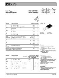
Inverse load current operation<br />
Maximum allowable load inductance for<br />
E AS = IL· L<br />
IL·RL<br />
(V<br />
2·R bb + |V OUT(CL) |) ln (1+<br />
L |V OUT(CL) | ) a single switch off<br />
L = f (I L ); T j,start = 150°C, V bb = 12 V, R L = 0 Ω<br />
V bb<br />
V<br />
bb<br />
- I L<br />
L [µH]<br />
+<br />
IN PROFET OUT<br />
100000<br />
-<br />
IS<br />
V OUT +<br />
V<br />
I IS<br />
IN<br />
10000<br />
-<br />
V IS R IS<br />
1000<br />
The device is specified for inverse load current<br />
operation (V OUT > V bb > 0V). The current sense<br />
feature is not available during this kind of operation<br />
100<br />
(I IS = 0). With I IN = 0 (e.g. input open) only the intrinsic<br />
drain source diode is conducting resulting in<br />
considerably increased power dissipation. If the<br />
10<br />
device is switched on (V IN = 0), this power<br />
dissipation is decreased to the much lower value<br />
R ON(INV) * I 2 (specifications see page 4).<br />
1<br />
Note: Temperature protection during inverse load<br />
current operation is not possible!<br />
1 10 100 1000<br />
I L [A]<br />
Inductive load switch-off energy<br />
Externally adjustable current limit<br />
dissipation<br />
If the device is conducting, the sense current can be<br />
E bb<br />
used to reduce the short circuit current and allow<br />
E AS<br />
higher lead inductance (see diagram above). The<br />
device will be turned off, if the threshold voltage of<br />
E Load T2 is reached by I<br />
V<br />
S<br />
*R IS<br />
. After a delay time defined<br />
bb<br />
by R<br />
i L(t)<br />
V<br />
*C V<br />
T1 will be reset. The device is turned on<br />
V bb<br />
again, the short circuit current is defined by I<br />
IN PROFET OUT<br />
L(SC)<br />
and<br />
the device is shut down after t d(SC)<br />
with latch<br />
E<br />
L function.<br />
IS<br />
L<br />
Z L<br />
{<br />
I IN<br />
R E<br />
V<br />
R L R<br />
bb<br />
IS<br />
V bb<br />
Energy stored in load inductance:<br />
IN PROFET OUT<br />
E L = 1 /2·L·I 2 L<br />
IS<br />
R<br />
While demagnetizing load inductance, the energy<br />
V<br />
R<br />
dissipated in PROFET is<br />
load<br />
IN<br />
E AS = E bb + E L - E R = V ON(CL)·i L (t) dt,<br />
Signal<br />
T1 C V T2<br />
R<br />
IS<br />
Signal<br />
GND<br />
<strong>Power</strong><br />
with an approximate solution for R L > 0 Ω:<br />
GND<br />
Infineon Technologies AG Page 10 2000-Mar-24

![AT89C1051 [ä¸ææ°æ®æå] [PDF] - ä¸æºåçæº](https://img.yumpu.com/44984295/1/184x260/at89c1051-a-aeaeaeraea-pdf-a-aeacae.jpg?quality=85)