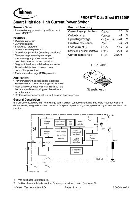
Smart Highside High Current Power Switch
Smart Highside High Current Power Switch
Smart Highside High Current Power Switch

Create successful ePaper yourself
Turn your PDF publications into a flip-book with our unique Google optimized e-Paper software.
PROFET® Data Sheet BTS550P<br />
<strong>Smart</strong> <strong><strong>High</strong>side</strong> <strong>High</strong> <strong>Current</strong> <strong>Power</strong> <strong>Switch</strong><br />
Reverse Save<br />
• Reverse battery protection by self turn on of<br />
power MOSFET<br />
Features<br />
• Overload protection<br />
• <strong>Current</strong> limitation<br />
• Short circuit protection<br />
• Overtemperature protection<br />
• Overvoltage protection (including load dump)<br />
• Clamp of negative voltage at output<br />
• Fast deenergizing of inductive loads 1)<br />
• Low ohmic inverse current operation<br />
• Diagnostic feedback with load current sense<br />
• Open load detection via current sense<br />
• Loss of Vbb protection 2)<br />
• Electrostatic discharge (ESD) protection<br />
Application<br />
• <strong>Power</strong> switch with current sense diagnostic<br />
feedback for 12 V and 24 V DC grounded loads<br />
• Most suitable for loads with high inrush current<br />
like lamps and motors; all types of resistive and<br />
inductive loads<br />
• Replaces electromechanical relays, fuses and discrete circuits<br />
Product Summary<br />
Overvoltage protection V bb(AZ) 62 V<br />
Output clamp V ON(CL) 44 V<br />
Operating voltage Vbb(on) 5.0 ... 34 V<br />
On-state resistance RON 3.6 mΩ<br />
Load current (ISO) IL(ISO) 115 A<br />
Short circuit current limitation IL(SC) 220 A<br />
<strong>Current</strong> sense ratio IL : I IS 21000<br />
TO-218AB/5<br />
1<br />
Straight leads<br />
General Description<br />
N channel vertical power FET with charge pump, current controlled input and diagnostic feedback with load<br />
current sense, integrated in <strong>Smart</strong> SIPMOS chip on chip technology. Fully protected by embedded protection<br />
functions.<br />
5<br />
3 & Tab<br />
Voltage<br />
source<br />
Overvoltage<br />
protection<br />
<strong>Current</strong><br />
limit<br />
Gate<br />
protection<br />
R bb<br />
+ V bb<br />
2<br />
IN<br />
ESD<br />
Voltage<br />
sensor<br />
Logic<br />
Charge pump<br />
Level shifter<br />
Rectifier<br />
Limit for<br />
unclamped<br />
ind. loads<br />
Output<br />
Voltage<br />
detection<br />
<strong>Current</strong><br />
Sense<br />
OUT<br />
1, 5<br />
I L<br />
Load<br />
I IN<br />
Temperature<br />
sensor<br />
V IN<br />
IS<br />
4<br />
I IS<br />
PROFET<br />
Load GND<br />
V IS<br />
R IS<br />
Logic GND<br />
1 ) With additional external diode.<br />
2) Additional external diode required for energized inductive loads (see page 9).<br />
Infineon Technologies AG Page 1 of 14 2000-Mar-24
Data Sheet BTS550P<br />
Pin Symbol Function<br />
1 OUT O Output to the load. The pins 1 and 5 must be shorted with each other<br />
especially in high current applications! 3)<br />
2 IN I Input, activates the power switch in case of short to ground<br />
3 Vbb +<br />
Positive power supply voltage, the tab is electrically connected to this pin.<br />
In high current applications the tab should be used for the V bb connection<br />
instead of this pin 4) .<br />
4 IS S Diagnostic feedback providing a sense current proportional to the load<br />
current; zero current on failure (see Truth Table on page 7)<br />
5 OUT O Output to the load. The pins 1 and 5 must be shorted with each other<br />
especially in high current applications! 3)<br />
Maximum Ratings at Tj = 25 °C unless otherwise specified<br />
Parameter Symbol Values Unit<br />
Supply voltage (overvoltage protection see page 4) V bb 40 V<br />
Supply voltage for short circuit protection,<br />
V bb 34 V<br />
T j,start =-40 ...+150°C: (E AS<br />
limitation see diagram on page 9)<br />
Load current (short circuit current, see page 5) I L self-limited A<br />
Load dump protection V LoadDump = U A + V s , U A = 13.5 V<br />
R<br />
5) I = 2 Ω, R L = 0.54 Ω, t d = 200 ms,<br />
6)<br />
V Load dump 80 V<br />
IN, IS = open or grounded<br />
Operating temperature range<br />
T j<br />
-40 ...+150 °C<br />
Storage temperature range<br />
T stg -55 ...+150<br />
<strong>Power</strong> dissipation (DC), T C ≤ 25 °C P tot 360 W<br />
Inductive load switch-off energy dissipation, single pulse<br />
V bb = 12V, T j,start = 150°C, T C = 150°C const.,<br />
E AS 3 J<br />
I L = 20 A, Z L = 15 mH, 0 Ω, see diagrams on page 10<br />
Electrostatic discharge capability (ESD)<br />
Human Body Model acc. MIL-STD883D, method 3015.7 and ESD<br />
assn. std. S5.1-1993, C = 100 pF, R = 1.5 kΩ<br />
V ESD 4 kV<br />
<strong>Current</strong> through input pin (DC)<br />
<strong>Current</strong> through current sense status pin (DC)<br />
see internal circuit diagrams on page 8<br />
I IN<br />
+15 , -250<br />
I IS +15 , -250<br />
mA<br />
3) Not shorting all outputs will considerably increase the on-state resistance, reduce the peak current capability<br />
and decrease the current sense accuracy<br />
4) Otherwise add up to 0.5 mΩ (depending on used length of the pin) to the R ON if the pin is used instead of the<br />
tab.<br />
5) R I = internal resistance of the load dump test pulse generator.<br />
6) V Load dump is setup without the DUT connected to the generator per ISO 7637-1 and DIN 40839.<br />
Infineon Technologies AG Page 2 2000-Mar-24
Thermal Characteristics<br />
Data Sheet BTS550P<br />
Parameter and Conditions Symbol Values Unit<br />
min typ max<br />
Thermal resistance chip - case: R thJC<br />
7) -- -- 0.35 K/W<br />
Junction - ambient (free air): R thJA -- 30 --<br />
Electrical Characteristics<br />
Parameter and Conditions Symbol Values Unit<br />
at Tj = -40 ... +150 °C, V bb = 12 V unless otherwise specified min typ max<br />
Load <strong>Switch</strong>ing Capabilities and Characteristics<br />
On-state resistance (Tab to pins 1,5, see measurement<br />
circuit page 8)<br />
I L = 20 A, T j = 25 °C:<br />
V IN = 0, I L = 20 A, T j = 150 °C:<br />
R ON -- 2.8<br />
5.0<br />
3.6<br />
6.5<br />
I L = 120 A, T j = 150 °C: -- 6.5<br />
V bb = 6V 8) , I L = 20 A, T j = 150 °C: R ON(Static) -- 7 10<br />
Nominal load current 9) (Tab to pins 1,5)<br />
I L(ISO) 90 115 -- A<br />
ISO 10483-1/6.7: V ON = 0.5 V, Tc = 85 °C 10)<br />
Maximum load current in resistive range<br />
(Tab to pins 1,5)<br />
see diagram on page 12<br />
V ON = 1.8 V, Tc = 25 °C:<br />
V ON = 1.8 V, Tc = 150 °C:<br />
Turn-on time 11) I IN to 90% V OUT :<br />
Turn-off time I IN to 10% V OUT :<br />
R L = 1 Ω , T j =-40...+150°C<br />
Slew rate on 11) (10 to 30% V OUT )<br />
R L = 1 Ω ,T j =25°C<br />
Slew rate off 11) (70 to 40% V OUT )<br />
R L = 1 Ω=,T j =25°C<br />
I L(Max) 390<br />
215<br />
t on 120<br />
t off 40<br />
--<br />
--<br />
250<br />
90<br />
600<br />
150<br />
mΩ<br />
--<br />
-- A<br />
µs<br />
dV/dt on 0.2 0.5 0.8 V/µs<br />
-dV/dt off 0.2 0.6 1 V/µs<br />
7) Thermal resistance R thCH case to heatsink (about 0.25 K/W with silicone paste) not included!<br />
8) Decrease of V bb below 10 V causes a slowly a dynamic increase of R ON to a higher value of R ON(Static) . As<br />
long as V bIN > V bIN(u) max , R ON increase is less than 10 % per second for T J < 85 °C.<br />
9) Not tested, specified by design.<br />
10) T J is about 105°C under these conditions.<br />
11) See timing diagram on page 13.<br />
Infineon Technologies AG Page 3 2000-Mar-24
Data Sheet BTS550P<br />
Parameter and Conditions Symbol Values Unit<br />
at Tj = -40 ... +150 °C, V bb = 12 V unless otherwise specified min typ max<br />
Inverse Load <strong>Current</strong> Operation<br />
On-state resistance (Pins 1,5 to pin 3)<br />
V bIN = 12 V, I L = - 20 A<br />
see diagram on page 10<br />
T j = 25 °C:<br />
T j = 150 °C:<br />
R ON(inv) -- 2.8<br />
5.0<br />
Nominal inverse load current (Pins 1,5 to Tab) I L(inv) 90 115 -- A<br />
V ON = -0.5 V, Tc = 85 °C 10<br />
Drain-source diode voltage (Vout<br />
I > Vbb)<br />
-V ON -- 0.6 0.7 V<br />
L = - 20 A, I IN = 0, Tj = +150°C<br />
3.6<br />
6.5<br />
mΩ<br />
Operating Parameters<br />
Operating voltage (V IN = 0) 8, 12) V bb(on) 5.0 -- 34 V<br />
Undervoltage shutdown 13) V bIN(u) 1.5 3.0 4.5 V<br />
Undervoltage start of charge pump<br />
see diagram page 14 V bIN(ucp) 3.0 4.5 6.0 V<br />
Overvoltage protection 14)<br />
T j =-40°C: V bIN(Z) 60 -- -- V<br />
I bb = 15 mA<br />
T j = 25...+150°C:<br />
62 64 --<br />
Standby current<br />
T j =-40...+25°C: I bb(off) -- 15 25 µA<br />
I IN = 0<br />
T j = 150°C:<br />
-- 25 50<br />
12) If the device is turned on before a Vbb -decrease, the operating voltage range is extended down to V bIN(u) . For<br />
the voltage range 0..34 V the device is fully protected against overtemperature and short circuit.<br />
13) VbIN = Vbb - VIN see diagram on page 8. When V bIN increases from less than V bIN(u) up to V bIN(ucp) = 5 V<br />
(typ.) the charge pump is not active and V OUT ≈V bb - 3 V.<br />
14) See also VON(CL) in circuit diagram on page 9.<br />
Infineon Technologies AG Page 4 2000-Mar-24
Data Sheet BTS550P<br />
Parameter and Conditions Symbol Values Unit<br />
at Tj = -40 ... +150 °C, V bb = 12 V unless otherwise specified min typ max<br />
Protection Functions<br />
Short circuit current limit (Tab to pins 1,5) 15<br />
VON = 12 V, time until shutdown max. 350 µs T c =-40°C:<br />
T c =25°C:<br />
T c =+150°C:<br />
Short circuit shutdown delay after input current<br />
positive slope, V ON > V ON(SC)<br />
min. value valid only if input "off-signal" time exceeds 30 µs<br />
Output clamp 16)<br />
I L = 40 mA:<br />
(inductive load switch off)<br />
Output clamp (inductive load switch off)<br />
at V OUT = V bb - V ON(CL) (e.g. overvoltage)<br />
I L = 40 mA<br />
I L(SCp) 100<br />
110<br />
120<br />
190<br />
220<br />
210<br />
350<br />
330<br />
310<br />
t d(SC) 80 -- 350 µs<br />
-V OUT(CL) 14 17 20 V<br />
V ON(CL) 40 44 47 V<br />
Short circuit shutdown detection voltage<br />
(pin 3 to pins 1,5) V ON(SC) -- 6 -- V<br />
Thermal overload trip temperature T jt 150 -- -- °C<br />
Thermal hysteresis ∆T jt -- 10 -- K<br />
Reverse Battery<br />
Reverse battery voltage 17) -V bb -- -- 32 V<br />
On-state resistance (Pins 1,5 to pin 3) T j = 25 °C: R ON(rev) -- 3.4 4.3<br />
V bb = -12V, V IN = 0, I L = - 20 A, R IS = 1 kΩ T j = 150 °C:<br />
-- 7.5<br />
mΩ<br />
Integrated resistor in Vbb line<br />
T j<br />
=25°C:<br />
T j<br />
=150°C:<br />
R bb 90<br />
105<br />
110<br />
125<br />
135<br />
150<br />
A<br />
Ω<br />
15 ) Short circuit is a failure mode. The device is not designed to operate continuously into a short circuit by<br />
permanent resetting the short circuit latch function. The lifetime will be reduced under such conditions.<br />
16) This output clamp can be "switched off" by using an additional diode at the IS-Pin (see page 8). If the diode<br />
is used, V OUT is clamped to V bb - V ON(CL) at inductive load switch off.<br />
17) The reverse load current through the intrinsic drain-source diode has to be limited by the connected load (as<br />
it is done with all polarity symmetric loads). Note that under off-conditions (IIN = IIS = 0) the power transistor<br />
is not activated. This results in raised power dissipation due to the higher voltage drop across the intrinsic<br />
drain-source diode. The temperature protection is not active during reverse current operation! Increasing<br />
reverse battery voltage capability is simply possible as described on page 9.<br />
Infineon Technologies AG Page 5 2000-Mar-24
Data Sheet BTS550P<br />
Parameter and Conditions Symbol Values Unit<br />
at Tj = -40 ... +150 °C, V bb = 12 V unless otherwise specified min typ max<br />
Diagnostic Characteristics<br />
<strong>Current</strong> sense ratio, I L = 120 A,T j =-40°C:<br />
static on-condition,<br />
T j =25°C:<br />
k ILIS = I L : I IS,<br />
T j =150°C:<br />
V ON < 1.5 V 18) ,<br />
I L = 20 A,T j =-40°C:<br />
V IS 4.0 V<br />
T j =150°C:<br />
see diagram on page 11 I L = 12 A,T j =-40°C:<br />
T j =25°C:<br />
T j =150°C:<br />
I L = 6 A,T j =-40°C:<br />
T j =25°C:<br />
T j =150°C:<br />
I IS<br />
=0 by I IN =0 (e.g. during deenergizing of inductive loads):<br />
k ILIS<br />
19 000<br />
19 000<br />
18 000<br />
18 500<br />
18 500<br />
18 000<br />
16 000<br />
17 000<br />
17 500<br />
12 000<br />
14 000<br />
16 000<br />
20 600<br />
20 500<br />
19 000<br />
22 300<br />
21 400<br />
19 500<br />
23 500<br />
22 000<br />
19 900<br />
28 000<br />
24 000<br />
20 500<br />
23 000<br />
22 500<br />
21 500<br />
26 000<br />
25 000<br />
23 000<br />
30 000<br />
26 500<br />
24 500<br />
46 000<br />
34 000<br />
30 000<br />
--<br />
Sense current saturation I IS,lim 6.5 -- -- mA<br />
<strong>Current</strong> sense leakage current<br />
I IN = 0: I IS(LL)<br />
-- 0.5 µA<br />
V IN = 0, I L ≤ 0: I IS(LH) -- 2 --<br />
<strong>Current</strong> sense settling time 19) t s(IS) -- -- 500 µs<br />
Overvoltage protection<br />
T j =-40°C: V bIS(Z) 60 -- -- V<br />
I bb = 15 mA<br />
T j = 25...+150°C:<br />
62 64 --<br />
Input<br />
Input and operating current (see diagram page 12) I IN(on) -- 0.8 1.5 mA<br />
IN grounded (V IN = 0)<br />
Input current for turn-off 20) I IN(off) -- -- 80 µA<br />
18) If V ON is higher, the sense current is no longer proportional to the load current due to sense current<br />
saturation, see I IS,lim .<br />
19) Not tested, specified by design.<br />
20) We recommend the resistance between IN and GND to be less than 0.5 kΩ for turn-on and more than<br />
500kΩ for turn-off. Consider that when the device is switched off (I IN = 0) the voltage between IN and GND<br />
reaches almost Vbb.<br />
Infineon Technologies AG Page 6 2000-Mar-24
Truth Table<br />
Data Sheet BTS550P<br />
Input<br />
current<br />
Output<br />
<strong>Current</strong><br />
Sense<br />
Remark<br />
Normal<br />
operation<br />
Very high<br />
load current<br />
<strong>Current</strong>limitation<br />
Short circuit to<br />
GND<br />
Overtemperature<br />
Short circuit to<br />
V bb<br />
Open load<br />
Negative output<br />
voltage clamp<br />
Inverse load<br />
current<br />
L = "Low" Level<br />
H = "<strong>High</strong>" Level<br />
level level I IS<br />
L<br />
H<br />
L<br />
H<br />
0<br />
nominal<br />
=I L / k ilis , up to I IS =I IS,lim<br />
up to V<br />
H H I ON =V ON(Fold back)<br />
IS, lim<br />
I IS no longer proportional to I L<br />
H H 0<br />
V ON > V ON(Fold back)<br />
if V ON >V ON(SC) , shutdown will occure<br />
L L<br />
0<br />
H L<br />
0<br />
L L<br />
0<br />
H L<br />
0<br />
L H<br />
0<br />
H H 150 °C, latch function 23)<br />
X<br />
Tj >150 °C, with auto-restart on cooling X<br />
Short circuit to GND protection<br />
switches off when V ON >6 V typ.<br />
(when first turned on after approx. 180 µs)<br />
Overvoltage shutdown - -<br />
Output negative voltage transient limit<br />
to V bb - V ON(CL) X X<br />
to V OUT = -19 V typ X 24) X 24)<br />
Overtemperature reset by cooling: Tj < Tjt (see diagram on page 14)<br />
Short circuit to GND: Shutdown remains latched until next reset via input (see diagram on page 13)<br />
X<br />
X<br />
21) Low ohmic short to Vbb may reduce the output current I L and can thus be detected via the sense current I IS .<br />
22) <strong>Power</strong> Transistor "OFF", potential defined by external impedance.<br />
23) Latch except when Vbb -V OUT < V ON(SC) after shutdown. In most cases V OUT = 0 V after shutdown (V OUT ≠<br />
0 V only if forced externally). So the device remains latched unless V bb < V ON(SC) (see page 5). No latch<br />
between turn on and t d(SC) .<br />
24) Can be "switched off" by using a diode DS (see page 8) or leaving open the current sense output.<br />
Infineon Technologies AG Page 7 2000-Mar-24
Data Sheet BTS550P<br />
Terms<br />
<strong>Current</strong> sense status output<br />
3<br />
V<br />
bb<br />
V ON<br />
V<br />
bb<br />
R bb<br />
ZD<br />
V<br />
Z,IS<br />
V bIN<br />
R IN<br />
V IN<br />
2<br />
V bIS<br />
IN<br />
V bb I bb I L V OUT<br />
PROFET<br />
4<br />
IS<br />
I IS<br />
OUT<br />
1,5<br />
I<br />
IS<br />
IS<br />
R<br />
IS<br />
V<br />
IS<br />
I IN<br />
V IS<br />
D S<br />
R IS<br />
Two or more devices can easily be connected in<br />
parallel to increase load current capability.<br />
R ON measurement layout<br />
≤ 5.5 mm<br />
V bb force contacts Out Force<br />
contacts<br />
(both out<br />
pins parallel)<br />
Sense<br />
contacts<br />
V Z,IS = 64 V (typ.), R IS = 1 kΩ nominal (or 1 kΩ /n, if<br />
n devices are connected in parallel). I S = I L /k ilis can<br />
be driven only by the internal circuit as long as V out -<br />
V IS > 5 V. If you want to measure load currents up<br />
to I L(M) , R IS should be less than V bb - 5 V<br />
I L(M) / K ilis<br />
.<br />
Note: For large values of R IS the voltage V IS can<br />
reach almost Vbb. See also overvoltage protection.<br />
If you don't use the current sense output in your<br />
application, you can leave it open.<br />
Short circuit detection<br />
Fault Condition: V ON > V ON(SC) (6 V typ.) and t> t d(SC)<br />
(80 ...350 µs).<br />
+ V bb<br />
V ON<br />
Input circuit (ESD protection)<br />
V bb<br />
Logic<br />
unit<br />
Short circuit<br />
detection<br />
OUT<br />
V Z,IN<br />
ZD<br />
R bb<br />
Inductive and overvoltage output clamp<br />
+ V bb<br />
V bIN<br />
IN<br />
V Z1<br />
I<br />
IN<br />
V ON<br />
V ZG<br />
OUT<br />
V IN<br />
When the device is switched off (I IN = 0) the<br />
voltage between IN and GND reaches almost Vbb.<br />
Use a mechanical switch, a bipolar or MOS<br />
transistor with appropriate breakdown voltage as<br />
driver. V Z,IN = 64 V (typ).<br />
D S<br />
IS<br />
PROFET<br />
V OUT<br />
VON is clamped to VON(Cl) = 42 V typ. At inductive<br />
load switch-off without D S , V OUT is clamped to<br />
Infineon Technologies AG Page 8 2000-Mar-24
V OUT(CL) = -19 V typ. via V ZG . With D S , V OUT is<br />
clamped to V bb - V ON(CL) via V Z1 . Using D S gives<br />
faster deenergizing of the inductive load, but higher<br />
peak power dissipation in the PROFET. In case of a<br />
floating ground with a potential higher than 19V<br />
referring to the OUT – potential the device will<br />
switch on, if diode DS is not used.<br />
Overvoltage protection of logic part<br />
Data Sheet BTS550P<br />
Vbb disconnect with energized<br />
inductive load<br />
Provide a current path with load current capability<br />
by using a diode, a Z-diode, or a varistor. (V ZL < 72<br />
V or V Zb < 30 V if R IN =0). For higher clamp voltages<br />
currents at IN and IS have to be limited to 250 mA.<br />
Version a:<br />
+ V bb<br />
V bb<br />
V<br />
bb<br />
V Z,IS<br />
R bb<br />
IN<br />
PROFET<br />
OUT<br />
R IN<br />
IN<br />
Logic<br />
IS<br />
V OUT<br />
V Z,IN<br />
R V<br />
V Z,VIS<br />
IS<br />
PROFET<br />
V ZL<br />
R IS<br />
Version b:<br />
Signal GND<br />
R bb = 120 Ω typ., V Z,IN = V Z,IS = 64 V typ., R IS = 1 kΩ<br />
nominal. Note that when overvoltage exceeds 69 V<br />
typ. a voltage above 5V can occur between IS and<br />
GND, if R V , V Z,VIS are not used.<br />
Reverse battery protection<br />
-V bb<br />
IN<br />
V<br />
bb<br />
PROFET<br />
IS<br />
OUT<br />
V bb<br />
V Zb<br />
R bb<br />
IN<br />
R IN<br />
Logic<br />
<strong>Power</strong><br />
Transistor<br />
OUT<br />
Note that there is no reverse battery protection<br />
when using a diode without additional Z-diode V ZL ,<br />
V Zb .<br />
D<br />
D S<br />
RIS<br />
IS<br />
RV<br />
R L<br />
Version c: Sometimes a neccessary voltage clamp<br />
is given by non inductive loads R L connected to the<br />
same switch and eliminates the need of clamping<br />
circuit:<br />
Signal GND<br />
<strong>Power</strong> GND<br />
R V ≥ 1 kΩ, R IS = 1 kΩ nominal. Add R IN for reverse<br />
battery protection in applications with Vbb above<br />
16 V 17) ; recommended value: 1 + 1 + 1 =<br />
R IN R IS R V<br />
0.1A<br />
|V bb | - 12V if D S is not used (or 1 0.1A<br />
=<br />
R IN |V bb | - 12V if<br />
D S is used).<br />
To minimize power dissipation at reverse battery<br />
operation, the summarized current into the IN and<br />
IS pin should be about 120mA. The current can be<br />
provided by using a small signal diode D in parallel<br />
to the input switch, by using a MOSFET input switch<br />
or by proper adjusting the current through R IS and<br />
R V .<br />
V bb<br />
IN<br />
V<br />
bb<br />
PROFET<br />
IS<br />
OUT<br />
R L<br />
Infineon Technologies AG Page 9 2000-Mar-24
Data Sheet BTS550P<br />
Inverse load current operation<br />
Maximum allowable load inductance for<br />
E AS = IL· L<br />
IL·RL<br />
(V<br />
2·R bb + |V OUT(CL) |) ln (1+<br />
L |V OUT(CL) | ) a single switch off<br />
L = f (I L ); T j,start = 150°C, V bb = 12 V, R L = 0 Ω<br />
V bb<br />
V<br />
bb<br />
- I L<br />
L [µH]<br />
+<br />
IN PROFET OUT<br />
100000<br />
-<br />
IS<br />
V OUT +<br />
V<br />
I IS<br />
IN<br />
10000<br />
-<br />
V IS R IS<br />
1000<br />
The device is specified for inverse load current<br />
operation (V OUT > V bb > 0V). The current sense<br />
feature is not available during this kind of operation<br />
100<br />
(I IS = 0). With I IN = 0 (e.g. input open) only the intrinsic<br />
drain source diode is conducting resulting in<br />
considerably increased power dissipation. If the<br />
10<br />
device is switched on (V IN = 0), this power<br />
dissipation is decreased to the much lower value<br />
R ON(INV) * I 2 (specifications see page 4).<br />
1<br />
Note: Temperature protection during inverse load<br />
current operation is not possible!<br />
1 10 100 1000<br />
I L [A]<br />
Inductive load switch-off energy<br />
Externally adjustable current limit<br />
dissipation<br />
If the device is conducting, the sense current can be<br />
E bb<br />
used to reduce the short circuit current and allow<br />
E AS<br />
higher lead inductance (see diagram above). The<br />
device will be turned off, if the threshold voltage of<br />
E Load T2 is reached by I<br />
V<br />
S<br />
*R IS<br />
. After a delay time defined<br />
bb<br />
by R<br />
i L(t)<br />
V<br />
*C V<br />
T1 will be reset. The device is turned on<br />
V bb<br />
again, the short circuit current is defined by I<br />
IN PROFET OUT<br />
L(SC)<br />
and<br />
the device is shut down after t d(SC)<br />
with latch<br />
E<br />
L function.<br />
IS<br />
L<br />
Z L<br />
{<br />
I IN<br />
R E<br />
V<br />
R L R<br />
bb<br />
IS<br />
V bb<br />
Energy stored in load inductance:<br />
IN PROFET OUT<br />
E L = 1 /2·L·I 2 L<br />
IS<br />
R<br />
While demagnetizing load inductance, the energy<br />
V<br />
R<br />
dissipated in PROFET is<br />
load<br />
IN<br />
E AS = E bb + E L - E R = V ON(CL)·i L (t) dt,<br />
Signal<br />
T1 C V T2<br />
R<br />
IS<br />
Signal<br />
GND<br />
<strong>Power</strong><br />
with an approximate solution for R L > 0 Ω:<br />
GND<br />
Infineon Technologies AG Page 10 2000-Mar-24
Characteristics<br />
Data Sheet BTS550P<br />
<strong>Current</strong> sense versus load current:<br />
I IS = f(I L )<br />
I IS [mA]<br />
7<br />
<strong>Current</strong> sense ratio:<br />
K ILIS = f(I L ), T J = 25 °C<br />
k ilis<br />
34000<br />
6<br />
32000<br />
5<br />
max<br />
30000<br />
28000<br />
4<br />
3<br />
26000<br />
24000<br />
max<br />
2<br />
min<br />
22000<br />
typ<br />
20000<br />
1<br />
0<br />
0 20 40 60 80 100 120<br />
18000<br />
min<br />
16000<br />
0 20 40 60 80 100 120<br />
<strong>Current</strong> sense ratio:<br />
K ILIS = f(I L ), T J = -40 °C<br />
K ilis<br />
46000<br />
44000<br />
42000<br />
40000<br />
38000<br />
36000<br />
34000<br />
32000<br />
30000<br />
28000<br />
26000<br />
24000<br />
22000<br />
20000<br />
18000<br />
16000<br />
14000<br />
max<br />
typ<br />
min<br />
I L [A]<br />
12000<br />
0 20 40 60 80 100 120<br />
<strong>Current</strong> sense ratio:<br />
K ILIS = f(I L ), T J = 150 °C<br />
K ilis<br />
30000<br />
28000<br />
26000<br />
24000<br />
22000<br />
20000<br />
18000<br />
max<br />
typ<br />
I L [A]<br />
min<br />
16000<br />
0 20 40 60 80 100 120<br />
I L [A]<br />
I L [A]<br />
Infineon Technologies AG Page 11 2000-Mar-24
Data Sheet BTS550P<br />
Typ. current limitation characteristic<br />
I L = f (VON, T j )<br />
I L [A]<br />
Typ. input current<br />
I IN = f (V bIN ), V bIN = V bb - V IN<br />
1.6<br />
1.4<br />
800<br />
700<br />
600<br />
500<br />
V ON > V ON(SC) only fort< t d( S C)<br />
(otherwise immediate shutdown)<br />
1.2<br />
1<br />
0.8<br />
400<br />
300<br />
T J = 25°C<br />
0.6<br />
0.4<br />
200<br />
100<br />
T J = -40°C<br />
T J = 150°C<br />
0.2<br />
0<br />
0 5 10 15 20<br />
V ON(FB)<br />
0<br />
0 20 40 60 80<br />
V ON [V]<br />
In case of V ON > V ON(SC) (typ. 6 V) the device will be<br />
switched off by internal short circuit detection.<br />
Typ. on-state resistance<br />
R ON = f (V bb , T j ); I L = 20 A; V IN = 0<br />
R ON [mOhm]<br />
10<br />
I IN [mA]<br />
V bIN [V]<br />
9<br />
8<br />
7<br />
6<br />
5<br />
4<br />
3<br />
2<br />
static<br />
dynamic<br />
T j<br />
= 150°C<br />
85°C<br />
25°C<br />
-40°C<br />
1<br />
0<br />
0 5 10 15 20 40<br />
V bb [V]<br />
Infineon Technologies AG Page 12 2000-Mar-24
Timing diagrams<br />
Figure 1a: <strong>Switch</strong>ing a resistive load,<br />
change of load current in on-condition:<br />
Figure 2b: <strong>Switch</strong>ing an inductive load:<br />
Data Sheet BTS550P<br />
I IN<br />
I IN<br />
V OUT<br />
dV/dtoff<br />
90%<br />
t on<br />
V OUT<br />
10%<br />
dV/dton<br />
t off<br />
I L<br />
I IS<br />
tslc(IS)<br />
tslc(IS)<br />
I L<br />
Load 1 Load 2<br />
t son(IS)<br />
t soff(IS)<br />
t<br />
I IS<br />
t<br />
The sense signal is not valid during a settling time<br />
after turn-on/off and after change of load current.<br />
Figure 3a: Short circuit:<br />
shut down by short circuit detection, reset by I IN = 0.<br />
Figure 2a: <strong>Switch</strong>ing motors and lamps:<br />
I IN<br />
I IN<br />
I L<br />
I L(SCp)<br />
V OUT<br />
t d(SC)<br />
I IL<br />
I IS<br />
V OUT >>0<br />
V OUT =0<br />
t<br />
I IS<br />
Sense current saturation can occur at very high<br />
inrush currents (see IIS,lim on page 6).<br />
t<br />
Shut down remains latched until next reset via input.<br />
Infineon Technologies AG Page 13 2000-Mar-24
Figure 4a: Overtemperature<br />
Reset if T j
Package and Ordering Code<br />
All dimensions in mm<br />
TO-218AB/5 Option E3146 Ordering code<br />
E3146<br />
Q67060-S6952A3<br />
Published by<br />
Infineon Technologies AG i Gr.,<br />
Bereichs Kommunikation<br />
St.-Martin-Strasse 76,<br />
D-81541 München<br />
© Infineon Technologies AG 1999<br />
All Rights Reserved.<br />
Data Sheet BTS550P<br />
Attention please!<br />
The information herein is given to describe certain<br />
components and shall not be considered as warranted<br />
characteristics.<br />
Terms of delivery and rights to technical change reserved.<br />
We hereby disclaim any and all warranties, including but not<br />
limited to warranties of non-infringement, regarding circuits,<br />
descriptions and charts stated herein.<br />
Infineon Technologies is an approved CECC manufacturer.<br />
Information<br />
For further information on technology, delivery terms and<br />
conditions and prices please contact your nearest Infineon<br />
Technologies Office in Germany or our Infineon<br />
Technologies Representatives worldwide (see address list).<br />
Warnings<br />
Due to technical requirements components may contain<br />
dangerous substances. For information on the types in<br />
question please contact your nearest Infineon Technologies<br />
Office.<br />
Infineon Technologies Components may only be used in lifesupport<br />
devices or systems with the express written approval<br />
of Infineon Technologies, if a failure of such components can<br />
reasonably be expected to cause the failure of that lifesupport<br />
device or system, or to affect the safety or<br />
effectiveness of that device or system. Life support devices<br />
or systems are intended to be implanted in the human body,<br />
or to support and/or maintain and sustain and/or protect<br />
human life. If they fail, it is reasonable to assume that the<br />
health of the user or other persons may be endangered.<br />
Infineon Technologies AG Page 15 2000-Mar-24
![AT89C1051 [ä¸ææ°æ®æå] [PDF] - ä¸æºåçæº](https://img.yumpu.com/44984295/1/184x260/at89c1051-a-aeaeaeraea-pdf-a-aeacae.jpg?quality=85)