

Arria V Device Handbook - Altera
Arria V Device Handbook - Altera
Arria V Device Handbook - Altera

Create successful ePaper yourself
Turn your PDF publications into a flip-book with our unique Google optimized e-Paper software.
<strong>Arria</strong> V <strong>Device</strong> <strong>Handbook</strong> Volume 1: <strong>Device</strong> Interfaces and<br />
Integration<br />
101 Innovation Drive<br />
San Jose, CA 95134<br />
www.altera.com<br />
AV-5V2-2.1<br />
<strong>Arria</strong> V <strong>Device</strong> <strong>Handbook</strong><br />
Volume 1: <strong>Device</strong> Interfaces and Integration
© 2012 <strong>Altera</strong> Corporation. All rights reserved. ALTERA, ARRIA, CYCLONE, HARDCOPY, MAX, MEGACORE, NIOS, QUARTUS and STRATIX words and logos<br />
are trademarks of <strong>Altera</strong> Corporation and registered in the U.S. Patent and Trademark Office and in other countries. All other words and logos identified as<br />
trademarks or service marks are the property of their respective holders as described at www.altera.com/common/legal.html. <strong>Altera</strong> warrants performance of its<br />
semiconductor products to current specifications in accordance with <strong>Altera</strong>'s standard warranty, but reserves the right to make changes to any products and<br />
services at any time without notice. <strong>Altera</strong> assumes no responsibility or liability arising out of the application or use of any information, product, or service<br />
described herein except as expressly agreed to in writing by <strong>Altera</strong>. <strong>Altera</strong> customers are advised to obtain the latest version of device specifications before relying<br />
on any published information and before placing orders for products or services.<br />
ISO<br />
9001:2008<br />
Registered<br />
June 2012 <strong>Altera</strong> Corporation <strong>Arria</strong> V <strong>Device</strong> <strong>Handbook</strong><br />
Volume 1: <strong>Device</strong> Interfaces and Integration
Contents<br />
Chapter Revision Dates ...................................................................... xi<br />
Section I. <strong>Device</strong> Core for <strong>Arria</strong> V <strong>Device</strong>s<br />
Revision History ........................................................................ I–1<br />
Chapter 1. Logic Array Blocks and Adaptive Logic Modules in <strong>Arria</strong> V <strong>Device</strong>s<br />
LAB ...................................................................................1–2<br />
MLAB ...............................................................................1–3<br />
Interconnects .........................................................................1–4<br />
LAB Control Signals ...................................................................1–5<br />
ALM Registers ........................................................................1–6<br />
ALM Outputs ........................................................................1–7<br />
ALM Operating Modes ..................................................................1–9<br />
Normal Mode ........................................................................1–9<br />
Extended LUT Mode ..................................................................1–9<br />
Arithmetic Mode .....................................................................1–10<br />
Carry Chain ......................................................................1–11<br />
Shared Arithmetic Mode ..............................................................1–12<br />
Shared Arithmetic Chain ...........................................................1–12<br />
Document Revision History .............................................................1–13<br />
Chapter 2. Memory Blocks in <strong>Arria</strong> V <strong>Device</strong>s<br />
Memory Types ..........................................................................2–1<br />
Memory Features ........................................................................2–2<br />
Memory Modes .........................................................................2–3<br />
Mixed-Width Port Configurations .........................................................2–4<br />
M10K Blocks Mixed-Width Configurations ...............................................2–4<br />
MLABs Mixed-Width Configurations ....................................................2–5<br />
Clocking Modes .........................................................................2–5<br />
Clocking Modes for Each Memory Mode .................................................2–5<br />
Asynchronous Clears ..................................................................2–5<br />
Output Read Data in Simultaneous Read/Write ...........................................2–6<br />
Independent Clock Enables ............................................................2–6<br />
Parity Bit ...............................................................................2–6<br />
Byte Enable .............................................................................2–6<br />
byteena Controls ......................................................................2–7<br />
Data Byte Output .....................................................................2–7<br />
RAM Blocks Operations ...............................................................2–8<br />
Design Considerations ...................................................................2–8<br />
Memory Block Selection ...............................................................2–8<br />
Conflict Resolution ....................................................................2–9<br />
Read-During-Write Behavior ...........................................................2–9<br />
Same-Port Read-During-Write Mode ..................................................2–9<br />
Mixed-Port Read-During-Write Mode ................................................2–10<br />
Power-Up State and Memory Initialization ..............................................2–12<br />
Power Management ..................................................................2–13<br />
Document Revision History .............................................................2–13<br />
June 2012 <strong>Altera</strong> Corporation <strong>Arria</strong> V <strong>Device</strong> <strong>Handbook</strong><br />
Volume 1: <strong>Device</strong> Interfaces and Integration
iv Contents<br />
Chapter 3. Variable-Precision DSP Blocks in <strong>Arria</strong> V <strong>Device</strong>s<br />
Features ................................................................................3–1<br />
Supported Operational Modes ............................................................3–2<br />
Design Considerations ...................................................................3–3<br />
Operational Modes ....................................................................3–3<br />
Pre-Adder ...........................................................................3–3<br />
Internal Coefficient ....................................................................3–3<br />
Accumulator .........................................................................3–3<br />
Chainout Adder ......................................................................3–3<br />
Block Architecture .......................................................................3–4<br />
Input Register Bank ...................................................................3–5<br />
Pre-Adder ...........................................................................3–6<br />
Internal Coefficient ....................................................................3–6<br />
Multipliers ...........................................................................3–7<br />
Adder ...............................................................................3–7<br />
Accumulator and Chainout Adder ......................................................3–7<br />
Systolic Registers .....................................................................3–8<br />
Double Accumulation Register .........................................................3–8<br />
Output Register Bank ..................................................................3–8<br />
Operational Mode Descriptions ...........................................................3–9<br />
Independent Multiplier Mode ..........................................................3–9<br />
Independent Complex Multiplier Mode .................................................3–12<br />
Multiplier Adder Sum Mode ..........................................................3–13<br />
18 x 18 Multiplication Summed with 36-Bit Input Mode ...................................3–14<br />
Systolic FIR Mode ....................................................................3–15<br />
Document Revision History .............................................................3–17<br />
Chapter 4. Clock Networks and PLLs in <strong>Arria</strong> V <strong>Device</strong>s<br />
Clock Networks in <strong>Arria</strong> V <strong>Device</strong>s ........................................................4–1<br />
Global Clock Networks ................................................................4–3<br />
Regional Clock Networks ..............................................................4–4<br />
Periphery Clock Networks .............................................................4–5<br />
Clock Sources Per Quadrant ............................................................4–6<br />
Clock Regions ........................................................................4–7<br />
Entire <strong>Device</strong> Clock Region ..........................................................4–7<br />
Regional Clock Region ..............................................................4–7<br />
Dual-Regional Clock Region .........................................................4–7<br />
Clock Network Sources ................................................................4–8<br />
Dedicated Clock Input Pins ..........................................................4–8<br />
Internal Logic ......................................................................4–8<br />
DPA Outputs ......................................................................4–8<br />
HSSI Outputs ......................................................................4–8<br />
PLL Clock Outputs .................................................................4–8<br />
Clock Input Pin Connections to GCLK and RCLK Networks .............................4–9<br />
Clock Output Connections ............................................................4–12<br />
Clock Control Block ..................................................................4–12<br />
GCLK Control Block ...............................................................4–13<br />
RCLK Control Block ...............................................................4–14<br />
PCLK Control Block ...............................................................4–14<br />
External PLL Clock Output Control Block .............................................4–15<br />
Clock Power Down ...................................................................4–16<br />
Clock Enable Signals .................................................................4–16<br />
<strong>Arria</strong> V PLLs ...........................................................................4–18<br />
<strong>Arria</strong> V <strong>Device</strong> <strong>Handbook</strong> June 2012 <strong>Altera</strong> Corporation<br />
Volume 1: <strong>Device</strong> Interfaces and Integration
Contents v<br />
Fractional PLL Architecture ...........................................................4–23<br />
Fractional PLL Usage ..............................................................4–23<br />
PLL External Clock I/O Pins ..........................................................4–23<br />
PLL Control Signals ..................................................................4–25<br />
pfdena ...........................................................................4–25<br />
areset ............................................................................4–25<br />
locked ............................................................................4–26<br />
Clock Feedback Modes ...............................................................4–26<br />
Source Synchronous Mode ..........................................................4–27<br />
LVDS Compensation Mode .........................................................4–28<br />
Direct Compensation Mode .........................................................4–29<br />
NormalMode .....................................................................4–30<br />
Zero-Delay Buffer Mode ............................................................4–30<br />
External Feedback Mode ...........................................................4–32<br />
Clock Multiplication and Division ......................................................4–33<br />
Programmable Duty Cycle ............................................................4–34<br />
Clock Switchover ....................................................................4–34<br />
Automatic Clock Switchover ........................................................4–35<br />
Manual Clock Switchover ..........................................................4–39<br />
Guidelines ........................................................................4–39<br />
PLL Reconfiguration and Dynamic Phase Shift ...........................................4–40<br />
Document Revision History .............................................................4–41<br />
Section II. I/O Interfaces for <strong>Arria</strong> V <strong>Device</strong>s<br />
Revision History ....................................................................... II–1<br />
Chapter 5. I/O Features in <strong>Arria</strong> V <strong>Device</strong>s<br />
I/O Standards Support ...................................................................5–2<br />
Design Considerations ...................................................................5–4<br />
I/O Bank Restrictions .................................................................5–4<br />
Non-Voltage-Referenced Standards ...................................................5–4<br />
Voltage-Referenced Standards ........................................................5–4<br />
Mixing Voltage-Referenced and Non-Voltage-Referenced Standards ......................5–4<br />
V CCPD Restriction .....................................................................5–5<br />
V CCIO Restriction .....................................................................5–5<br />
V REF Pin Restriction ...................................................................5–5<br />
3.3-V I/O Interface ....................................................................5–5<br />
LVDS Channels .......................................................................5–6<br />
I/O Banks ..............................................................................5–6<br />
Modular I/O Banks ...................................................................5–8<br />
IOE Structure ..........................................................................5–11<br />
Current Strength .....................................................................5–12<br />
MultiVolt I/O Interface ...............................................................5–13<br />
Programmable IOE Features .............................................................5–14<br />
Slew-Rate Control ....................................................................5–14<br />
I/O Delay ...........................................................................5–14<br />
Programmable IOE Delay ...........................................................5–14<br />
Programmable Output Buffer Delay ..................................................5–15<br />
Open-Drain Output ..................................................................5–15<br />
Bus-Hold ...........................................................................5–15<br />
Pull-Up Resistor .....................................................................5–16<br />
Pre-Emphasis ........................................................................5–16<br />
Differential Output Voltage ...........................................................5–16<br />
June 2012 <strong>Altera</strong> Corporation <strong>Arria</strong> V <strong>Device</strong> <strong>Handbook</strong><br />
Volume 1: <strong>Device</strong> Interfaces and Integration
vi Contents<br />
OCT Schemes ..........................................................................5–17<br />
OCT Calibration Block ................................................................5–18<br />
Sharing an OCT Calibration Block on Multiple I/O Banks ...............................5–21<br />
R S OCT with Calibration ..............................................................5–22<br />
R S OCT Without Calibration ...........................................................5–22<br />
R T OCT with Calibration ..............................................................5–23<br />
Dynamic OCT .......................................................................5–24<br />
LVDS Input R D OCT .................................................................5–25<br />
I/O Standards Termination Schemes ......................................................5–26<br />
Single-Ended I/O Standard Termination ................................................5–28<br />
Differential I/O Standard Termination ..................................................5–29<br />
LVDS, RSDS, and Mini-LVDS I/O Standard Termination ...............................5–31<br />
LVPECL I/O Standard Termination ..................................................5–32<br />
Emulated LVDS, RSDS, and Mini-LVDS I/O Standard Termination ......................5–32<br />
Document Revision History .............................................................5–34<br />
Chapter 6. High-Speed Differential I/O Interfaces and DPA in <strong>Arria</strong> V <strong>Device</strong>s<br />
Dedicated High-Speed I/O Circuitries .....................................................6–1<br />
SERDES and DPA Bank Locations .......................................................6–2<br />
LVDS SERDES Circuitry ...............................................................6–3<br />
LVDS Channels .......................................................................6–4<br />
True LVDS Buffers ....................................................................6–4<br />
Differential Transmitter ..................................................................6–6<br />
Transmitter Blocks ....................................................................6–6<br />
Transmitter Clocking ..................................................................6–6<br />
Serializer Bypass for DDR and SDR Operations ...........................................6–7<br />
Programmable V OD .....................................................................................6–8<br />
Programmable Pre-Emphasis ...........................................................6–8<br />
Differential Receiver .....................................................................6–9<br />
Receiver Blocks ......................................................................6–10<br />
DPA Block ........................................................................6–10<br />
Synchronizer ......................................................................6–11<br />
Data Realignment Block (Bit Slip) ....................................................6–12<br />
Deserializer .......................................................................6–13<br />
Receiver Modes ......................................................................6–13<br />
Non-DPAMode ...................................................................6–14<br />
DPAMode .......................................................................6–15<br />
Soft-CDR Mode ...................................................................6–16<br />
Receiver Clocking ....................................................................6–17<br />
Differential I/O Termination ..........................................................6–17<br />
PLLs and Clocking .....................................................................6–18<br />
Source Synchronous Timing Budget ......................................................6–18<br />
Differential Data Orientation ..........................................................6–19<br />
Differential I/O Bit Position ...........................................................6–19<br />
Transmitter Channel-to-Channel Skew ..................................................6–20<br />
Receiver Skew Margin for Non-DPA Mode ..............................................6–21<br />
Design Considerations ..................................................................6–21<br />
Differential Pin Placement .............................................................6–21<br />
DPA-Enabled Channels, DPA-Disabled Channels, and Single-Ended I/Os ................6–22<br />
Guidelines for DPA-Enabled Differential Channels .....................................6–22<br />
Guidelines for DPA-Disabled Differential Channels ....................................6–25<br />
Document Revision History .............................................................6–28<br />
<strong>Arria</strong> V <strong>Device</strong> <strong>Handbook</strong> June 2012 <strong>Altera</strong> Corporation<br />
Volume 1: <strong>Device</strong> Interfaces and Integration
Contents vii<br />
Chapter 7. External Memory Interfaces in <strong>Arria</strong> V <strong>Device</strong>s<br />
Memory Interface Pin Support ............................................................7–2<br />
Design Considerations ...................................................................7–5<br />
Memory Interface .....................................................................7–5<br />
Delay-Locked Loop ...................................................................7–5<br />
DQ/DQS Pins ........................................................................7–6<br />
Using the RZQ Pins in a DQ/DQS Group for Memory Interfaces ............................7–6<br />
PHYCLK Networks ...................................................................7–6<br />
DDR2 SDRAM Interface ...............................................................7–6<br />
DDR3 SDRAM DIMM .................................................................7–7<br />
Hard Memory Controller ..............................................................7–7<br />
Bonding ...........................................................................7–7<br />
External Memory Interface Features .......................................................7–8<br />
DQS Phase-Shift Circuitry ..............................................................7–9<br />
Delay-Locked Loop ................................................................7–11<br />
DLL Phase-Shift ...................................................................7–11<br />
PHY Clock (PHYCLK) Networks .......................................................7–13<br />
DQS Logic Block .....................................................................7–16<br />
Update Enable Circuitry ............................................................7–16<br />
DQS Delay Chain ..................................................................7–17<br />
DQS Postamble Circuitry ...........................................................7–17<br />
HDR Block .......................................................................7–17<br />
Dynamic OCT Control ................................................................7–18<br />
IOE Registers ........................................................................7–19<br />
Input Registers ....................................................................7–19<br />
Output Registers ..................................................................7–19<br />
Delay Chain .........................................................................7–21<br />
Hard Memory Controllers .............................................................7–22<br />
Features of the Hard Memory Controller .............................................7–22<br />
Multiport Logic ...................................................................7–24<br />
Bonding Support ..................................................................7–24<br />
UniPHY IP ............................................................................7–28<br />
Document Revision History .............................................................7–28<br />
Section III. System Integration for <strong>Arria</strong> V <strong>Device</strong>s<br />
Revision History ...................................................................... III–1<br />
Chapter 8. Configuration, Design Security, and Remote System Upgrades in <strong>Arria</strong> V <strong>Device</strong>s<br />
MSEL Pin Settings .......................................................................8–2<br />
Configuration Sequence ..................................................................8–3<br />
PowerUp ............................................................................8–4<br />
V CCPGM Pin........................................................................8–4<br />
V CCPD Pin .........................................................................8–4<br />
Reset ................................................................................8–4<br />
Configuration ........................................................................8–4<br />
Configuration Error Handling ..........................................................8–5<br />
Initialization .........................................................................8–5<br />
User Mode ...........................................................................8–5<br />
<strong>Device</strong> Configuration Pins ................................................................8–6<br />
Configuration Pins Summary ...........................................................8–6<br />
Configuration Pin Options in the Quartus II Software ......................................8–7<br />
Fast Passive Parallel Configuration ........................................................8–7<br />
FPP Single-<strong>Device</strong> Configuration ........................................................8–8<br />
June 2012 <strong>Altera</strong> Corporation <strong>Arria</strong> V <strong>Device</strong> <strong>Handbook</strong><br />
Volume 1: <strong>Device</strong> Interfaces and Integration
viii Contents<br />
FPP Multi-<strong>Device</strong> Configuration ........................................................8–8<br />
Pin Connections and Guidelines ......................................................8–8<br />
Using Multiple Configuration Data ...................................................8–9<br />
Configuring Multiple <strong>Device</strong>s Using One Configuration Data ...........................8–10<br />
Active Serial Configuration ..............................................................8–11<br />
DATA Clock (DCLK) .................................................................8–11<br />
AS Single-<strong>Device</strong> Configuration .......................................................8–12<br />
AS Multi-<strong>Device</strong> Configuration ........................................................8–13<br />
Pin Connections and Guidelines .....................................................8–13<br />
Using Multiple Configuration Data ..................................................8–14<br />
Configuring Multiple <strong>Device</strong>s Using One Configuration Data ...........................8–15<br />
Estimating the AS Configuration Time ..................................................8–15<br />
Using EPCS and EPCQ <strong>Device</strong>s ........................................................8–16<br />
Controlling EPCS and EPCQ <strong>Device</strong>s .................................................8–16<br />
Trace Length and Loading ..........................................................8–16<br />
Programming EPCS and EPCQ <strong>Device</strong>s ..............................................8–17<br />
Passive Serial Configuration .............................................................8–21<br />
PS Single-<strong>Device</strong> Configuration ........................................................8–21<br />
PS Multi-<strong>Device</strong> Configuration ........................................................8–23<br />
Pin Connections and Guidelines .....................................................8–23<br />
Using Multiple Configuration Data ..................................................8–23<br />
Configuring Multiple <strong>Device</strong>s Using One Configuration Data ...........................8–24<br />
Using PC Host and Download Cable .................................................8–25<br />
JTAG Configuration ....................................................................8–26<br />
JTAG Single-<strong>Device</strong> Configuration .....................................................8–26<br />
JTAG Multi-<strong>Device</strong> Configuration ......................................................8–29<br />
CONFIG_IO JTAG Instruction .........................................................8–30<br />
Configuration Data Compression .........................................................8–30<br />
Enabling Compression Before Design Compilation .......................................8–30<br />
Enabling Compression After Design Compilation ........................................8–31<br />
Using Compression in Multi-<strong>Device</strong> Configuration .......................................8–31<br />
Remote System Upgrades ...............................................................8–32<br />
Configuration Images ................................................................8–32<br />
Configuration Sequence ..............................................................8–33<br />
Remote System Upgrade Circuitry .....................................................8–34<br />
Enabling Remote System Upgrade Circuitry .............................................8–35<br />
Remote System Upgrade Registers .....................................................8–35<br />
Control Register ...................................................................8–36<br />
Status Register ....................................................................8–36<br />
Remote System Upgrade State Machine .................................................8–36<br />
User Watchdog Timer ................................................................8–37<br />
Design Security ........................................................................8–37<br />
JTAG Secure Mode ...................................................................8–38<br />
Security Key Types ...................................................................8–39<br />
Security Modes ......................................................................8–39<br />
Design Security Implementation Steps ..................................................8–40<br />
Document Revision History .............................................................8–41<br />
Chapter 9. SEU Mitigation in <strong>Arria</strong> V <strong>Device</strong>s<br />
Basic Description ........................................................................9–1<br />
Error Detection Features .................................................................9–1<br />
Types of Error Detection .................................................................9–2<br />
Configuration Error Detection ..........................................................9–2<br />
User Mode Error Detection .............................................................9–2<br />
<strong>Arria</strong> V <strong>Device</strong> <strong>Handbook</strong> June 2012 <strong>Altera</strong> Corporation<br />
Volume 1: <strong>Device</strong> Interfaces and Integration
Contents ix<br />
Error Detection Components ..............................................................9–3<br />
Error Detection Pin ....................................................................9–3<br />
Error Detection Registers ...............................................................9–3<br />
Error Message Register ................................................................9–5<br />
Storage Size for Error Detection .........................................................9–5<br />
Error Detection Timing ...................................................................9–6<br />
Minimum EMR Update Interval ........................................................9–6<br />
Error Detection Frequency .............................................................9–6<br />
CRC Calculation Time .................................................................9–7<br />
Using the Error Detection Feature .........................................................9–8<br />
Enabling the User Mode Error Detection .................................................9–8<br />
Error Detection Process ................................................................9–8<br />
Reading the Error Location Bit Through JTAG ............................................9–9<br />
Recovering From CRC Errors ...........................................................9–9<br />
Testing the Error Detection Block ..........................................................9–9<br />
Error Detection Instruction .............................................................9–9<br />
JTAG Fault Injection Register ..........................................................9–10<br />
Automating the Testing Process ........................................................9–10<br />
Document Revision History .............................................................9–10<br />
Chapter 10. JTAG Boundary-Scan Testing in <strong>Arria</strong> V <strong>Device</strong>s<br />
BST Operation Control ..................................................................10–1<br />
IDCODE ............................................................................10–1<br />
Supported JTAG Instruction ...........................................................10–2<br />
JTAG Secure Mode ................................................................10–4<br />
JTAG Private Instruction ..............................................................10–4<br />
I/O Voltage for JTAG Operation .........................................................10–4<br />
Enabling and Disabling IEEE Std. 1149.1 BST Circuitry ......................................10–5<br />
Performing BST ........................................................................10–5<br />
Guidelines for IEEE Std. 1149.1 Boundary-Scan Testing ......................................10–6<br />
IEEE Std. 1149.1 BST Architecture ........................................................10–7<br />
IEEE Std. 1149.1 BST Functionality .....................................................10–7<br />
IEEE Std. 1149.1 BST Circuitry Registers ................................................10–7<br />
IEEE Std. 1149.1 BST Pin Function ......................................................10–8<br />
IEEE Std. 1149.1 Boundary-Scan Register ................................................10–9<br />
Boundary-Scan Cells of a <strong>Arria</strong> V <strong>Device</strong> I/O Pin ......................................10–9<br />
IEEE Std. 1149.1 TAP Controller ......................................................10–11<br />
IEEE Std. 1149.1 JTAG Mandatory Instruction .............................................10–14<br />
SAMPLE/PRELOAD Instruction Mode ................................................10–14<br />
EXTEST Instruction Mode ............................................................10–16<br />
BYPASS Instruction Mode ............................................................10–18<br />
Document Revision History ............................................................10–19<br />
Chapter 11. Power Management in <strong>Arria</strong> V <strong>Device</strong>s<br />
Power Consumption ....................................................................11–2<br />
Internal Temperature Sensing Diode ......................................................11–2<br />
Hot-Socketing Feature ..................................................................11–3<br />
Hot-Socketing Implementation ...........................................................11–4<br />
Power-Up Sequencing ..................................................................11–5<br />
Power-On Reset Circuitry ...............................................................11–6<br />
Document Revision History .............................................................11–8<br />
June 2012 <strong>Altera</strong> Corporation <strong>Arria</strong> V <strong>Device</strong> <strong>Handbook</strong><br />
Volume 1: <strong>Device</strong> Interfaces and Integration
x Contents<br />
Additional Information<br />
How to Contact <strong>Altera</strong> ................................................................ Info–1<br />
Typographic Conventions ............................................................. Info–1<br />
<strong>Arria</strong> V <strong>Device</strong> <strong>Handbook</strong> June 2012 <strong>Altera</strong> Corporation<br />
Volume 1: <strong>Device</strong> Interfaces and Integration
Chapter Revision Dates<br />
The chapters in this document, Volume 1: <strong>Device</strong> Interfaces and Integration, were<br />
revised on the following dates. Where chapters or groups of chapters are available<br />
separately, part numbers are listed.<br />
Part Number:<br />
Chapter 1. Logic Array Blocks and Adaptive Logic Modules in <strong>Arria</strong> V <strong>Device</strong>s<br />
Revised: June 2012<br />
Part Number: AV-52001-2.0<br />
Chapter 2. Memory Blocks in <strong>Arria</strong> V <strong>Device</strong>s<br />
Revised: June 2012<br />
Part Number: AV-52002-2.0<br />
Chapter 3. Variable-Precision DSP Blocks in <strong>Arria</strong> V <strong>Device</strong>s<br />
Revised: June 2012<br />
Part Number: AV-52003-2.0<br />
Chapter 4. Clock Networks and PLLs in <strong>Arria</strong> V <strong>Device</strong>s<br />
Revised: June 2012<br />
Part Number: AV-52004-2.0<br />
Chapter 5. I/O Features in <strong>Arria</strong> V <strong>Device</strong>s<br />
Revised: June 2012<br />
Part Number: AV52005-2.0<br />
Chapter 6. High-Speed Differential I/O Interfaces and DPA in <strong>Arria</strong> V <strong>Device</strong>s<br />
Revised: June 2012<br />
Part Number: AV52006-2.0<br />
Chapter 7. External Memory Interfaces in <strong>Arria</strong> V <strong>Device</strong>s<br />
Revised: June 2012<br />
Part Number: AV52007-2.0<br />
Chapter 8. Configuration, Design Security, and Remote System Upgrades in <strong>Arria</strong> V <strong>Device</strong>s<br />
Revised: June 2012<br />
Part Number: AV-52008-2.0<br />
Chapter 9. SEU Mitigation in <strong>Arria</strong> V <strong>Device</strong>s<br />
Revised: June 2012<br />
Part Number: AV-52009-2.0<br />
Chapter 10. JTAG Boundary-Scan Testing in <strong>Arria</strong> V <strong>Device</strong>s<br />
Revised: June 2012<br />
Part Number: AV-52010-2.0<br />
Chapter 11. Power Management in <strong>Arria</strong> V <strong>Device</strong>s<br />
Revised: June 2012<br />
Part Number: AV-52011-2.0<br />
June 2012 <strong>Altera</strong> Corporation <strong>Arria</strong> V <strong>Device</strong> <strong>Handbook</strong><br />
Volume 1: <strong>Device</strong> Interfaces and Integration
xii<br />
<strong>Arria</strong> V <strong>Device</strong> <strong>Handbook</strong> June 2012 <strong>Altera</strong> Corporation<br />
Volume 1: <strong>Device</strong> Interfaces and Integration
Revision History<br />
© 2012 <strong>Altera</strong> Corporation. All rights reserved. ALTERA, ARRIA, CYCLONE, HARDCOPY, MAX, MEGACORE, NIOS, QUARTUS and STRATIX words and logos<br />
are trademarks of <strong>Altera</strong> Corporation and registered in the U.S. Patent and Trademark Office and in other countries. All other words and logos identified as<br />
trademarks or service marks are the property of their respective holders as described at www.altera.com/common/legal.html. <strong>Altera</strong> warrants performance of its<br />
semiconductor products to current specifications in accordance with <strong>Altera</strong>'s standard warranty, but reserves the right to make changes to any products and<br />
services at any time without notice. <strong>Altera</strong> assumes no responsibility or liability arising out of the application or use of any information, product, or service<br />
described herein except as expressly agreed to in writing by <strong>Altera</strong>. <strong>Altera</strong> customers are advised to obtain the latest version of device specifications before relying<br />
on any published information and before placing orders for products or services.<br />
<strong>Arria</strong> V <strong>Device</strong> <strong>Handbook</strong><br />
Volume 1: <strong>Device</strong> Interfaces and Integration<br />
June 2012<br />
Section I. <strong>Device</strong> Core for <strong>Arria</strong> V <strong>Device</strong>s<br />
This section provides a complete overview of all features relating to the <strong>Arria</strong> ® V<br />
device family. This section includes the following chapters:<br />
■ Chapter 1, Logic Array Blocks and Adaptive Logic Modules in <strong>Arria</strong> V <strong>Device</strong>s<br />
■ Chapter 2, Memory Blocks in <strong>Arria</strong> V <strong>Device</strong>s<br />
■ Chapter 3, Variable-Precision DSP Blocks in <strong>Arria</strong> V <strong>Device</strong>s<br />
■ Chapter 4, Clock Networks and PLLs in <strong>Arria</strong> V <strong>Device</strong>s<br />
Refer to each chapter for its own specific revision history. For information about when<br />
each chapter was updated, refer to the Chapter Revision Dates section, which appears<br />
in this volume.<br />
ISO<br />
9001:2008<br />
Registered
I–2<br />
Revision History<br />
<strong>Arria</strong> V <strong>Device</strong> <strong>Handbook</strong> June 2012 <strong>Altera</strong> Corporation<br />
Volume 1: <strong>Device</strong> Interfaces and Integration
June 2012<br />
AV-52001-2.0<br />
AV-52001-2.0<br />
© 2012 <strong>Altera</strong> Corporation. All rights reserved. ALTERA, ARRIA, CYCLONE, HARDCOPY, MAX, MEGACORE, NIOS, QUARTUS and STRATIX words and logos<br />
are trademarks of <strong>Altera</strong> Corporation and registered in the U.S. Patent and Trademark Office and in other countries. All other words and logos identified as<br />
trademarks or service marks are the property of their respective holders as described at www.altera.com/common/legal.html. <strong>Altera</strong> warrants performance of its<br />
semiconductor products to current specifications in accordance with <strong>Altera</strong>'s standard warranty, but reserves the right to make changes to any products and<br />
services at any time without notice. <strong>Altera</strong> assumes no responsibility or liability arising out of the application or use of any information, product, or service<br />
described herein except as expressly agreed to in writing by <strong>Altera</strong>. <strong>Altera</strong> customers are advised to obtain the latest version of device specifications before relying<br />
on any published information and before placing orders for products or services.<br />
<strong>Arria</strong> V <strong>Device</strong> <strong>Handbook</strong><br />
Volume 1: <strong>Device</strong> Interfaces and Integration<br />
June 2012<br />
1. Logic Array Blocks and Adaptive Logic<br />
Modules in <strong>Arria</strong> V <strong>Device</strong>s<br />
This chapter describes the features of the logic array block (LAB) in the <strong>Arria</strong> ® V core<br />
fabric.<br />
The LAB is composed of basic building blocks known as adaptive logic modules<br />
(ALMs) that you can configure to implement logic functions, arithmetic functions,<br />
and register functions.<br />
You can use a quarter of the available LABs in <strong>Arria</strong> V devices as a memory LAB<br />
(MLAB).<br />
The Quartus ® II software and other supported third-party synthesis tools, in<br />
conjunction with parameterized functions such as the library of parameterized<br />
modules (LPM), automatically choose the appropriate mode for common functions<br />
such as counters, adders, subtractors, and arithmetic functions.<br />
This chapter contains the following sections:<br />
■ “LAB”<br />
■ “ALM Operating Modes” on page 1–9<br />
ISO<br />
9001:2008<br />
Registered<br />
Feedback Subscribe
1–2 Chapter 1: Logic Array Blocks and Adaptive Logic Modules in <strong>Arria</strong> V <strong>Device</strong>s<br />
LAB<br />
LAB<br />
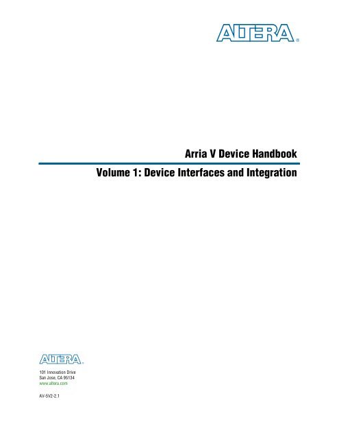
The LABs are configurable logic blocks that consist of a group of logic resources. Each<br />
LAB contains dedicated logic for driving control signals to its ALMs.<br />
MLAB is a superset of the LAB and includes all the LAB features.<br />
Figure 1–1 shows an overview of the <strong>Arria</strong> V LAB and MLAB structure with the LAB<br />
interconnects.<br />
Figure 1–1. LAB Structure and Interconnects Overview in <strong>Arria</strong> V <strong>Device</strong>s<br />
R14<br />
R3/R6<br />
Direct link<br />
interconnect from<br />
adjacent block (1)<br />
Direct link<br />
interconnect to<br />
adjacent block<br />
Local interconnect<br />
LAB<br />
C2/C4 C12<br />
Row interconnects of<br />
variable speed and length<br />
MLAB<br />
Fast local interconnect is driven<br />
from either sides by column interconnect<br />
and LABs, and from above by row interconnect<br />
Note to Figure 1–1:<br />
(1) Connects to adjacent LABs, memory blocks, digital signal processing (DSP) blocks, or I/O element (IOE) outputs.<br />
Column interconnects of<br />
variable speed and length<br />
<strong>Arria</strong> V <strong>Device</strong> <strong>Handbook</strong> June 2012 <strong>Altera</strong> Corporation<br />
Volume 1: <strong>Device</strong> Interfaces and Integration<br />
ALMs<br />
Direct link<br />
interconnect from<br />
adjacent block<br />
Direct link<br />
interconnect to<br />
adjacent block
Chapter 1: Logic Array Blocks and Adaptive Logic Modules in <strong>Arria</strong> V <strong>Device</strong>s 1–3<br />
LAB<br />
MLAB<br />
Each MLAB supports a maximum of 640 bits of simple dual-port SRAM.<br />
You can configure each ALM in an MLAB as a 32 x 2 memory block, resulting in a<br />
configuration of 32 x 20 simple dual-port SRAM blocks.<br />
Figure 1–2 shows the LAB and MLAB topology.<br />
Figure 1–2. LAB and MLAB Structure for <strong>Arria</strong> V <strong>Device</strong>s<br />
(1)<br />
LUT-based-32 x 2<br />
Simple dual port SRAM<br />
(1)<br />
LUT-based-32 x 2<br />
Simple dual port SRAM<br />
LUT-based-32 x 2 (1)<br />
Simple dual port SRAM<br />
LUT-based-32 x 2 (1)<br />
Simple dual port SRAM<br />
LUT-based-32 x 2 (1)<br />
Simple dual port SRAM<br />
LUT-based-32 x 2<br />
(1)<br />
Simple dual port SRAM<br />
LUT-based-32 x 2 (1)<br />
Simple dual port SRAM<br />
LUT-based-32 x 2<br />
(1)<br />
Simple dual port SRAM<br />
LUT-based-32 x 2 (1)<br />
Simple dual port SRAM<br />
LUT-based-32 x 2 (1)<br />
Simple dual port SRAM<br />
MLAB LAB<br />
Note to Figure 1–2:<br />
(1) You can use an MLAB ALM as a regular LAB ALM or configure it as a dual-port SRAM.<br />
June 2012 <strong>Altera</strong> Corporation <strong>Arria</strong> V <strong>Device</strong> <strong>Handbook</strong><br />
Volume 1: <strong>Device</strong> Interfaces and Integration<br />
ALM<br />
ALM<br />
ALM<br />
ALM<br />
ALM<br />
LAB Control Block LAB Control Block<br />
ALM<br />
ALM<br />
ALM<br />
ALM<br />
ALM
1–4 Chapter 1: Logic Array Blocks and Adaptive Logic Modules in <strong>Arria</strong> V <strong>Device</strong>s<br />
LAB<br />
Interconnects<br />
Each LAB can drive 30 ALMs through fast-local and direct-link interconnects. Ten<br />
ALMs are in any given LAB and ten ALMs are in each of the adjacent LABs.<br />
The local interconnect can drive ALMs in the same LAB using column and row<br />
interconnects and ALM outputs in the same LAB.<br />
Neighboring LABs, MLABs, M10K blocks, or digital signal processing (DSP) blocks<br />
from the left or right can also drive the LAB’s local interconnect using the direct link<br />
connection.<br />
The direct link connection feature minimizes the use of row and column<br />
interconnects, providing higher performance and flexibility.<br />
Figure 1–3 shows the LAB fast-local and direct-link interconnects.<br />
Figure 1–3. Direct Link and Fast Local Interconnects for <strong>Arria</strong> V <strong>Device</strong>s<br />
Direct link<br />
interconnect<br />
to left<br />
Direct link interconnect from<br />
left LAB, memory block,<br />
DSP block, or IOE output<br />
ALMs ALMs<br />
MLAB<br />
Fast local<br />
interconnect<br />
<strong>Arria</strong> V <strong>Device</strong> <strong>Handbook</strong> June 2012 <strong>Altera</strong> Corporation<br />
Volume 1: <strong>Device</strong> Interfaces and Integration<br />
LAB<br />
Direct link interconnect from<br />
right LAB, memory block,<br />
DSP block, or IOE output<br />
Direct link<br />
interconnect<br />
to right
Chapter 1: Logic Array Blocks and Adaptive Logic Modules in <strong>Arria</strong> V <strong>Device</strong>s 1–5<br />
LAB<br />
LAB Control Signals<br />
Each LAB contains dedicated logic for driving the control signals to its ALMs, and has<br />
two unique clock sources and three clock enable signals.<br />
The LAB control block generates up to three clocks using the two clock sources and<br />
three clock enable signals. Each clock and the clock enable signals are linked.<br />
De-asserting the clock enable signal turns off the corresponding LAB-wide clock.<br />
Figure 1–4 shows the clock sources and clock enable signals in an LAB.<br />
Figure 1–4. LAB-Wide Control Signals for <strong>Arria</strong> V <strong>Device</strong>s (1)<br />
Dedicated Row LAB Clocks<br />
Local Interconnect<br />
Local Interconnect<br />
Local Interconnect<br />
Local Interconnect<br />
Note to Figure 1–4:<br />
(1) For more information, refer to Figure 1–6 on page 1–8.<br />
6<br />
6<br />
6<br />
There are two unique<br />
clock signals per LAB.<br />
labclk0 labclk1 labclk2 syncload<br />
labclr1<br />
labclkena0<br />
or asyncload<br />
or labpreset<br />
labclkena1 labclkena2 labclr0 synclr<br />
June 2012 <strong>Altera</strong> Corporation <strong>Arria</strong> V <strong>Device</strong> <strong>Handbook</strong><br />
Volume 1: <strong>Device</strong> Interfaces and Integration
1–6 Chapter 1: Logic Array Blocks and Adaptive Logic Modules in <strong>Arria</strong> V <strong>Device</strong>s<br />
LAB<br />
ALM Registers<br />
One ALM contains four programmable registers. Each register has data, clock,<br />
synchronous and asynchronous clear, and synchronous load functions.<br />
Global signals, general-purpose I/O (GPIO) pins, or any internal logic can drive the<br />
clock and clear control signals of an ALM register.<br />
GPIO pins or internal logic drives the clock enable signal.<br />
For combinational functions, the registers are bypassed and the output of the look-up<br />
table (LUT) drives directly to the outputs of an ALM.<br />
Figure 1–5 shows a high-level block diagram of the <strong>Arria</strong> V ALM.<br />
Figure 1–5. High-Level Block Diagram of the <strong>Arria</strong> V ALM<br />
dataf0<br />
datae0<br />
dataa<br />
datab<br />
datac<br />
datad<br />
datae1<br />
dataf1<br />
shared_arith_in<br />
6-Input LUT<br />
6-Input LUT<br />
shared_arith_out<br />
carry_in<br />
adder0<br />
adder1<br />
carry_out<br />
Combinational/<br />
Memory ALUT0<br />
Combinational/<br />
Memory ALUT1<br />
reg_chain_in<br />
1 The Quartus II software automatically configures the ALMs for optimized<br />
performance.<br />
<strong>Arria</strong> V <strong>Device</strong> <strong>Handbook</strong> June 2012 <strong>Altera</strong> Corporation<br />
Volume 1: <strong>Device</strong> Interfaces and Integration<br />
labclk<br />
reg_chain_out<br />
D Q<br />
reg0<br />
D Q<br />
reg1<br />
D Q<br />
reg2<br />
D Q<br />
reg3<br />
To general or<br />
local routing<br />
To general or<br />
local routing<br />
To general or<br />
local routing<br />
To general or<br />
local routing<br />
To general or<br />
local routing<br />
To general or<br />
local routing<br />
To general or<br />
local routing<br />
To general or<br />
local routing
Chapter 1: Logic Array Blocks and Adaptive Logic Modules in <strong>Arria</strong> V <strong>Device</strong>s 1–7<br />
LAB<br />
ALM Outputs<br />
The LUT, adder, or register output can drive the ALM outputs. There are two sets of<br />
outputs—general routing outputs and register chain outputs.<br />
For each set of output drivers, two ALM outputs can drive column, row, or direct link<br />
routing connections, and one of these ALM outputs can also drive local interconnect<br />
resources. The LUT or adder can drive one output while the register drives another<br />
output.<br />
Register packing improves device utilization by allowing unrelated register and<br />
combinational logic to be packed into a single ALM. Another mechanism to improve<br />
fitting is to allow the register output to feed back into the look-up table (LUT) of the<br />
same ALM so that the register is packed with its own fan-out LUT. The ALM can also<br />
drive out registered and unregistered versions of the LUT or adder output.<br />
June 2012 <strong>Altera</strong> Corporation <strong>Arria</strong> V <strong>Device</strong> <strong>Handbook</strong><br />
Volume 1: <strong>Device</strong> Interfaces and Integration
1–8 Chapter 1: Logic Array Blocks and Adaptive Logic Modules in <strong>Arria</strong> V <strong>Device</strong>s<br />
LAB<br />
Figure 1–6 shows a detailed view of all the connections in an ALM.<br />
Figure 1–6. ALM Connection Details for <strong>Arria</strong> V <strong>Device</strong>s<br />
dataf0<br />
datae0<br />
dataa<br />
datab<br />
datac0<br />
datac1<br />
datae1<br />
dataf1<br />
shared_arith_in<br />
4-Input<br />
LUT<br />
3-Input<br />
LUT<br />
3-Input<br />
LUT<br />
4-Input<br />
LUT<br />
3-Input<br />
LUT<br />
3-Input<br />
LUT<br />
shared_arith_out<br />
carry_in<br />
+<br />
+<br />
carry_out<br />
GND<br />
VCC<br />
syncload<br />
aclr[1:0]<br />
clk[2:0] sclr reg_chain_in<br />
D Q<br />
D Q<br />
<strong>Arria</strong> V <strong>Device</strong> <strong>Handbook</strong> June 2012 <strong>Altera</strong> Corporation<br />
Volume 1: <strong>Device</strong> Interfaces and Integration<br />
CLR<br />
CLR<br />
D Q<br />
CLR<br />
CLR<br />
D Q<br />
row, column<br />
direct link routing<br />
row, column<br />
direct link routing<br />
local<br />
interconnect<br />
row, column<br />
direct link routing<br />
row, column<br />
direct link routing<br />
local<br />
interconnect<br />
reg_chain_out
Chapter 1: Logic Array Blocks and Adaptive Logic Modules in <strong>Arria</strong> V <strong>Device</strong>s 1–9<br />
ALM Operating Modes<br />
ALM Operating Modes<br />
Normal Mode<br />
The <strong>Arria</strong> V ALM operates in any of the following modes:<br />
■ Normal Mode<br />
■ Extended LUT Mode<br />
■ Arithmetic Mode<br />
■ Shared Arithmetic Mode<br />
Up to eight data inputs from the LAB local interconnect are inputs to the<br />
combinational logic. Normal mode allows two functions to be implemented in one<br />
<strong>Arria</strong> V ALM, or a single function of up to six inputs.<br />
The ALM can support certain combinations of completely independent functions and<br />
various combinations of functions that have common inputs.<br />
Extended LUT Mode<br />
In this mode, if the 7-input function is unregistered, the unused eighth input is<br />
available for register packing.<br />
1 Functions that fit into the template, as shown in Figure 1–7, often appear in designs as<br />
“if-else” statements in Verilog HDL or VHDL code.<br />
Figure 1–7 shows the template of supported 7-input functions using extended LUT<br />
mode.<br />
Figure 1–7. Template for Supported 7-Input Functions in Extended LUT Mode in <strong>Arria</strong> V <strong>Device</strong>s<br />
datae0<br />
datac<br />
dataa<br />
datab<br />
datad<br />
dataf0<br />
datae1<br />
dataf1<br />
5-Input<br />
LUT<br />
5-Input<br />
LUT<br />
This input is available<br />
for register packing.<br />
combout0<br />
June 2012 <strong>Altera</strong> Corporation <strong>Arria</strong> V <strong>Device</strong> <strong>Handbook</strong><br />
Volume 1: <strong>Device</strong> Interfaces and Integration<br />
D Q<br />
reg0<br />
To gener al or<br />
local routing<br />
To gener al or<br />
local routing
1–10 Chapter 1: Logic Array Blocks and Adaptive Logic Modules in <strong>Arria</strong> V <strong>Device</strong>s<br />
ALM Operating Modes<br />
Arithmetic Mode<br />
The ALM in arithmetic mode uses two sets of two 4-input LUTs along with two<br />
dedicated full adders.<br />
The dedicated adders allow the LUTs to perform pre-adder logic; therefore, each<br />
adder can add the output of two 4-input functions.<br />
The ALM supports simultaneous use of the adder’s carry output along with<br />
combinational logic outputs. The adder output is ignored in this operation.<br />
Using the adder with the combinational logic output provides resource savings of up<br />
to 50% for functions that can use this mode.<br />
Figure 1–8 shows an ALM in arithmetic mode.<br />
Figure 1–8. ALM in Arithmetic Mode for <strong>Arria</strong> V <strong>Device</strong>s<br />
datae0<br />
dataf0<br />
datac<br />
datab<br />
dataa<br />
datad<br />
datae1<br />
dataf1<br />
<strong>Arria</strong> V <strong>Device</strong> <strong>Handbook</strong> June 2012 <strong>Altera</strong> Corporation<br />
Volume 1: <strong>Device</strong> Interfaces and Integration<br />
4-Input<br />
LUT<br />
4-Input<br />
LUT<br />
4-Input<br />
LUT<br />
4-Input<br />
LUT<br />
carry_in<br />
carry_out<br />
adder0<br />
adder1<br />
D Q<br />
reg0<br />
D Q<br />
reg1<br />
D Q<br />
reg2<br />
D Q<br />
reg3<br />
To general or<br />
local routing<br />
To general or<br />
local routing<br />
To general or<br />
local routing<br />
To general or<br />
local routing<br />
To general or<br />
local routing<br />
To general or<br />
local routing<br />
To general or<br />
local routing<br />
To general or<br />
local routing
Chapter 1: Logic Array Blocks and Adaptive Logic Modules in <strong>Arria</strong> V <strong>Device</strong>s 1–11<br />
ALM Operating Modes<br />
Carry Chain<br />
The carry chain provides a fast carry function between the dedicated adders in<br />
arithmetic or shared arithmetic mode.<br />
The two-bit carry select feature in <strong>Arria</strong> V devices halves the propagation delay of<br />
carry chains within the ALM. Carry chains can begin in either the first ALM or the<br />
fifth ALM in a LAB. The final carry-out signal is routed to an ALM, where it is fed to<br />
local, row, or column interconnects.<br />
To avoid routing congestion in one small area of the device when a high fan-in<br />
arithmetic function is implemented, the LAB can support carry chains that only use<br />
either the top half or bottom half of the LAB before connecting to the next LAB. This<br />
leaves the other half of the ALMs in the LAB available for implementing narrower<br />
fan-in functions in normal mode. Carry chains that use the top five ALMs in the first<br />
LAB carry into the top half of the ALMs in the next LAB in the column. Carry chains<br />
that use the bottom five ALMs in the first LAB carry into the bottom half of the ALMs<br />
in the next LAB within the column. You can bypass the top-half of the LAB columns<br />
and bottom-half of the MLAB columns.<br />
The Quartus II Compiler creates carry chains longer than 20 ALMs (10 ALMs in<br />
arithmetic or shared arithmetic mode) by linking LABs together automatically. For<br />
enhanced fitting, a long carry chain runs vertically, allowing fast horizontal<br />
connections to the TriMatrix memory and DSP blocks. A carry chain can continue as<br />
far as a full column.<br />
June 2012 <strong>Altera</strong> Corporation <strong>Arria</strong> V <strong>Device</strong> <strong>Handbook</strong><br />
Volume 1: <strong>Device</strong> Interfaces and Integration
1–12 Chapter 1: Logic Array Blocks and Adaptive Logic Modules in <strong>Arria</strong> V <strong>Device</strong>s<br />
ALM Operating Modes<br />
Shared Arithmetic Mode<br />
The ALM in shared arithmetic mode can implement a 3-input add in the ALM.<br />
This mode configures the ALM with four 4-input LUTs. Each LUT either computes<br />
the sum of three inputs or the carry of three inputs. The output of the carry<br />
computation is fed to the next adder using a dedicated connection called the shared<br />
arithmetic chain.<br />
Figure 1–9 shows the ALM using this feature.<br />
Figure 1–9. ALM in Shared Arithmetic Mode for <strong>Arria</strong> V <strong>Device</strong>s<br />
datae0<br />
datac<br />
datab<br />
dataa<br />
datad<br />
datae1<br />
shared_arith_in<br />
shared_arith_out<br />
Shared Arithmetic Chain<br />
The shared arithmetic chain available in enhanced arithmetic mode allows the ALM<br />
to implement a 3-input adder. This significantly reduces the resources necessary to<br />
implement large adder trees or correlator functions.<br />
Similar to carry chains, the top and bottom half of the shared arithmetic chains in<br />
alternate LAB columns can be bypassed. This capability allows the shared arithmetic<br />
chain to cascade through half of the ALMs in an LAB while leaving the other half<br />
available for narrower fan-in functionality. In every LAB column is top-half<br />
bypassable; while in MLAB columns are bottom-half bypassable.<br />
The shared arithmetic chain can begin in either the first or sixth ALM in an LAB. The<br />
Quartus II Compiler creates shared arithmetic chains longer than 20 ALMs (10 ALMs<br />
in arithmetic or shared arithmetic mode) by linking LABs together automatically. To<br />
enhanced fitting, a long shared arithmetic chain runs vertically, allowing fast<br />
horizontal connections to the TriMatrix memory and DSP blocks. A shared arithmetic<br />
chain can continue as far as a full column.<br />
<strong>Arria</strong> V <strong>Device</strong> <strong>Handbook</strong> June 2012 <strong>Altera</strong> Corporation<br />
Volume 1: <strong>Device</strong> Interfaces and Integration<br />
4-Input<br />
LUT<br />
4-Input<br />
LUT<br />
4-Input<br />
LUT<br />
4-Input<br />
LUT<br />
carry_in<br />
carry_out<br />
labclk<br />
D Q<br />
reg0<br />
D Q<br />
reg1<br />
D Q<br />
reg2<br />
D Q<br />
reg3<br />
To general or<br />
local routing<br />
To general or<br />
local routing<br />
To general or<br />
local routing<br />
To general or<br />
local routing<br />
To general or<br />
local routing<br />
To general or<br />
local routing<br />
To general or<br />
local routing<br />
To general or<br />
local routing
Chapter 1: Logic Array Blocks and Adaptive Logic Modules in <strong>Arria</strong> V <strong>Device</strong>s 1–13<br />
Document Revision History<br />
Document Revision History<br />
Table 1–1. Document Revision History<br />
Table 1–1 lists the revision history for this chapter.<br />
Date Version Changes<br />
June 2012 2.0<br />
Updated for the Quartus II software v12.0 release:<br />
■ Restructured chapter.<br />
■ Updated Figure 1–6.<br />
November 2011 1.1 Restructured chapter.<br />
May 2011 1.0 Initial release.<br />
June 2012 <strong>Altera</strong> Corporation <strong>Arria</strong> V <strong>Device</strong> <strong>Handbook</strong><br />
Volume 1: <strong>Device</strong> Interfaces and Integration
1–14 Chapter 1: Logic Array Blocks and Adaptive Logic Modules in <strong>Arria</strong> V <strong>Device</strong>s<br />
Document Revision History<br />
<strong>Arria</strong> V <strong>Device</strong> <strong>Handbook</strong> June 2012 <strong>Altera</strong> Corporation<br />
Volume 1: <strong>Device</strong> Interfaces and Integration
June 2012<br />
AV-52002-2.0<br />
AV-52002-2.0<br />
Memory Types<br />
© 2012 <strong>Altera</strong> Corporation. All rights reserved. ALTERA, ARRIA, CYCLONE, HARDCOPY, MAX, MEGACORE, NIOS, QUARTUS and STRATIX words and logos<br />
are trademarks of <strong>Altera</strong> Corporation and registered in the U.S. Patent and Trademark Office and in other countries. All other words and logos identified as<br />
trademarks or service marks are the property of their respective holders as described at www.altera.com/common/legal.html. <strong>Altera</strong> warrants performance of its<br />
semiconductor products to current specifications in accordance with <strong>Altera</strong>'s standard warranty, but reserves the right to make changes to any products and<br />
services at any time without notice. <strong>Altera</strong> assumes no responsibility or liability arising out of the application or use of any information, product, or service<br />
described herein except as expressly agreed to in writing by <strong>Altera</strong>. <strong>Altera</strong> customers are advised to obtain the latest version of device specifications before relying<br />
on any published information and before placing orders for products or services.<br />
<strong>Arria</strong> V <strong>Device</strong> <strong>Handbook</strong><br />
Volume 1: <strong>Device</strong> Interfaces and Integration<br />
June 2012<br />
2. Memory Blocks in <strong>Arria</strong> V <strong>Device</strong>s<br />
This chapter describes the embedded memory blocks in <strong>Arria</strong> ® V devices.<br />
The memory blocks in <strong>Arria</strong> V devices provide different sizes of embedded SRAM to<br />
fit your design requirements.<br />
This chapter contains the following sections:<br />
■ “Memory Types” on page 2–1<br />
■ “Memory Features” on page 2–2<br />
■ “Memory Modes” on page 2–3<br />
■ “Mixed-Width Port Configurations” on page 2–4<br />
■ “Clocking Modes” on page 2–5<br />
■ “Parity Bit” on page 2–6<br />
■ “Byte Enable” on page 2–6<br />
■ “Design Considerations” on page 2–8<br />
The <strong>Arria</strong> V devices contain two types of memory blocks:<br />
■ M10K blocks—10-kilobit (Kb) blocks of dedicated memory resources that you can<br />
use to create designs with large memory configurations.<br />
■ Memory logic array blocks (MLABs)—640-bit enhanced memory blocks that are<br />
configured from dual-purpose logic array blocks (LABs). The MLABs are<br />
optimized for implementation of shift registers for digital signal processing (DSP)<br />
applications, wide shallow FIFO buffers, and filter delay lines. Each MLAB is<br />
made up of ten adaptive logic modules (ALMs) that you can configure as ten<br />
32 x 2 blocks, giving you one 32 x 20 simple dual-port SRAM block per MLAB.<br />
f For information about the embedded memory capacity available in each <strong>Arria</strong> V<br />
device, refer to the <strong>Arria</strong> V <strong>Device</strong> Overview.<br />
ISO<br />
9001:2008<br />
Registered<br />
Feedback Subscribe
2–2 Chapter 2: Memory Blocks in <strong>Arria</strong> V <strong>Device</strong>s<br />
Memory Features<br />
Memory Features<br />
Table 2–1 summarizes the features supported by the memory blocks.<br />
Table 2–1. Memory Features in <strong>Arria</strong> V <strong>Device</strong>s<br />
Feature M10K MLAB<br />
Maximum operating frequency 400 MHz 500 MHz<br />
Total RAM bits (including parity bits) 10,240 640<br />
Configuration (depth × width)<br />
256 x 32, 256 x 40,<br />
512 x 16, 512 x 20,<br />
1K x 8, 1K x 10,<br />
2K x 4, 2K x 5,<br />
4K x 2, and 8K x 1<br />
32 x 16, 32 x 18, and 32 x 20<br />
Parity bits Yes Yes<br />
Byte enable Yes Yes<br />
Packed mode Yes —<br />
Address clock enable Yes Yes<br />
Memory modes<br />
■ Single-port memory<br />
■ Simple dual-port memory<br />
■ True dual-port memory<br />
■ Embedded shift register<br />
■ ROM<br />
■ FIFO buffer<br />
■ Single-port memory<br />
■ Simple dual-port memory<br />
■ Embedded shift register<br />
■ ROM<br />
■ FIFO buffer<br />
Simple dual-port mixed width Yes —<br />
True dual-port mixed width Yes —<br />
FIFO buffer mixed width Yes —<br />
Memory Initialization File (.mif) Yes Yes<br />
Mixed-clock mode Yes Yes<br />
■ Registered output ports—Cleared.<br />
Power-up state Output ports are cleared.<br />
■ Unregistered output ports—Read<br />
memory contents.<br />
Asynchronous clears Output registers<br />
Write/Read operation triggering Rising clock edges<br />
Same-port read-during-write<br />
Mixed-port read-during-write<br />
Output ports set to “new data” or<br />
“don’t care”.<br />
(The “don’t care” mode applies only for<br />
the single-port RAM mode.)<br />
Output ports set to “old data” or “don’t<br />
care”.<br />
Output ports set to “don’t care”.<br />
Output ports set to “old data”, “new<br />
data”, “don’t care”, or “constrained don’t<br />
care”.<br />
ECC support Soft IP support using the Quartus ® II software.<br />
Fully synchronous memory Yes Yes<br />
Asynchronous memory —<br />
Only for flow-through read memory<br />
operations.<br />
<strong>Arria</strong> V <strong>Device</strong> <strong>Handbook</strong> June 2012 <strong>Altera</strong> Corporation<br />
Volume 1: <strong>Device</strong> Interfaces and Integration
Chapter 2: Memory Blocks in <strong>Arria</strong> V <strong>Device</strong>s 2–3<br />
Memory Modes<br />
Memory Modes<br />
Table 2–2 lists and describes the memory modes that are supported in the <strong>Arria</strong> V<br />
memory blocks.<br />
c To avoid corrupting the memory contents, do not violate the setup or hold time on<br />
any of the memory block input registers during read or write operations. This is<br />
applicable if you use the memory blocks in single-port RAM, simple dual-port RAM,<br />
true dual-port RAM, or ROM mode.<br />
Table 2–2. Memory Modes Supported in the Memory Blocks<br />
Memory Mode Description and Additional Information<br />
Single-port RAM<br />
Simple dual-port<br />
RAM<br />
True dual-port RAM<br />
Shift-register<br />
ROM<br />
FIFO<br />
You can perform only one read or one write operation at a time.<br />
Use the read enable port to control the RAM output ports behavior during a write operation:<br />
■ To retain the previous values that are held during the most recent active read enable—Create a<br />
read-enable port and perform the write operation with the read enable port deasserted.<br />
■ To show the new data being written, the old data at that address, or a “Don't Care” value when<br />
read-during-write occurs at the same address location—Do not create a read-enable signal, or<br />
activate the read enable during a write operation.<br />
You can simultaneously perform one read and one write operations to different locations where the<br />
write operation happens on port A and the read operation happens on port B.<br />
You can perform any combination of two port operations: two reads, two writes, or one read and<br />
one write at two different clock frequencies. This mode is available only for M10K blocks.<br />
You can use the memory blocks as a shift-register block to save logic cells and routing resources.<br />
This is useful in DSP applications that require local data storage such as finite impulse response<br />
(FIR) filters, pseudo-random number generators, multi-channel filtering, and auto- and crosscorrelation<br />
functions. Traditionally, the local data storage is implemented with standard flip-flops<br />
that exhaust many logic cells for large shift registers.<br />
You can use the memory blocks as ROM.<br />
■ Initialize the ROM contents of the memory blocks using a .mif or .hex.<br />
■ The address lines of the ROM are registered on M10K blocks but can be unregistered on MLABs.<br />
■ The outputs can be registered or unregistered.<br />
■ The output registers can be asynchronously cleared.<br />
■ The ROM read operation is identical to the read operation in the single-port RAM configuration.<br />
You can use the memory blocks as FIFO buffers.<br />
Use the SCFIFO and DCFIFO megafunctions to implement single- and dual-clock asynchronous FIFO<br />
buffers in your design.<br />
For designs with many small and shallow FIFO buffers, the MLABs are ideal for the FIFO mode.<br />
However, the MLABs do not support mixed-width FIFO mode.<br />
f For more information about each memory mode, refer to the Internal Memory (RAM<br />
and ROM) User Guide.<br />
f For more information about implementing the shift register mode, refer to the<br />
RAM-Based Shift Register (ALTSHIFT_TAPS) Megafunction User Guide.<br />
June 2012 <strong>Altera</strong> Corporation <strong>Arria</strong> V <strong>Device</strong> <strong>Handbook</strong><br />
Volume 1: <strong>Device</strong> Interfaces and Integration
2–4 Chapter 2: Memory Blocks in <strong>Arria</strong> V <strong>Device</strong>s<br />
Mixed-Width Port Configurations<br />
f For more information about implementing FIFO buffers, refer to the SCFIFO and<br />
DCFIFO Megafunctions User Guide.<br />
Mixed-Width Port Configurations<br />
The mixed-width port configuration is supported in the simple dual-port RAM and<br />
true dual-port RAM memory modes.<br />
f For more information about dual-port mixed width support, refer to the Internal<br />
Memory (RAM and ROM) User Guide.<br />
M10K Blocks Mixed-Width Configurations<br />
Table 2–3 lists the mixed-width configurations of the M10K blocks in the simple dualport<br />
RAM mode.<br />
Table 2–3. M10K Block Mixed-Width Configurations (Simple Dual-Port RAM Mode)<br />
Read Port<br />
8K x 1<br />
4K x 2<br />
2K x 4<br />
Write Port<br />
Table 2–4 lists the mixed-width configurations of the M10K blocks in true dual-port<br />
mode.<br />
<strong>Arria</strong> V <strong>Device</strong> <strong>Handbook</strong> June 2012 <strong>Altera</strong> Corporation<br />
Volume 1: <strong>Device</strong> Interfaces and Integration<br />
2K x 5<br />
8K x 1 Yes Yes Yes — Yes — Yes — Yes —<br />
4K x 2 Yes Yes Yes — Yes — Yes — Yes —<br />
2K x 4 Yes Yes Yes — Yes — Yes — Yes —<br />
2K x 5 — — — Yes — Yes — Yes — Yes<br />
1K x 8 Yes Yes Yes — Yes — Yes — Yes —<br />
1K x 10 — — — Yes — Yes — Yes — Yes<br />
512 x 16 Yes Yes Yes — Yes — Yes — Yes —<br />
512 x 20 — — — Yes — Yes — Yes — Yes<br />
256 x 32 Yes Yes Yes — Yes — Yes — Yes —<br />
256 x 40 — — — Yes — Yes — Yes — Yes<br />
Table 2–4. M10K Block Mixed-Width Configurations (True Dual-Port Mode) (Part 1 of 2)<br />
Port B<br />
8K x 1<br />
4K x 2<br />
2K x 4<br />
1K x 8<br />
Port A<br />
8K x 1 Yes Yes Yes — Yes — Yes —<br />
4K x 2 Yes Yes Yes — Yes — Yes —<br />
2K x 4 Yes Yes Yes — Yes — Yes —<br />
2K x 5 — — — Yes — Yes — Yes<br />
1K x 8 Yes Yes Yes — Yes — Yes —<br />
1K x 10 — — — Yes — Yes — Yes<br />
2K x 5<br />
1K x 10<br />
1K x 8<br />
512 x 16<br />
1K x 10<br />
512 x 20<br />
512 x 16<br />
256 x 32<br />
256 x 40<br />
512 x 20
Chapter 2: Memory Blocks in <strong>Arria</strong> V <strong>Device</strong>s 2–5<br />
Clocking Modes<br />
MLABs Mixed-Width Configurations<br />
Clocking Modes<br />
Table 2–4. M10K Block Mixed-Width Configurations (True Dual-Port Mode) (Part 2 of 2)<br />
Port B<br />
MLABs do not have native support for mixed-width operation. However, if you select<br />
AUTO for your memory block type in the parameter editor, the Quartus II software<br />
can implement mixed-width memories in MLABs by using more than one MLAB.<br />
This section describes the clocking modes for the <strong>Arria</strong> V memory blocks.<br />
c To avoid corrupting the memory contents, do not violate the setup or hold time on the<br />
memory block address registers during read or write operations.<br />
Clocking Modes for Each Memory Mode<br />
Table 2–5 lists the memory blocks clocking modes supported in the <strong>Arria</strong> V devices<br />
and the memory modes supported by each clocking mode.<br />
f For more information about each clocking mode, refer to the Internal Memory (RAM<br />
and ROM) User Guide.<br />
Asynchronous Clears<br />
8K x 1<br />
4K x 2<br />
Port A<br />
512 x 16 Yes Yes Yes — Yes — Yes —<br />
512 x 20 — — — Yes — Yes — Yes<br />
In all clocking modes, asynchronous clears are available only for output latches and<br />
output registers. For the independent clock mode, this is applicable on both ports.<br />
June 2012 <strong>Altera</strong> Corporation <strong>Arria</strong> V <strong>Device</strong> <strong>Handbook</strong><br />
Volume 1: <strong>Device</strong> Interfaces and Integration<br />
2K x 4<br />
2K x 5<br />
1K x 8<br />
Table 2–5. Memory Blocks Clocking Modes for Each Memory Mode<br />
Clocking Mode<br />
Single-Port<br />
Simple<br />
Dual-Port<br />
Memory Mode<br />
True<br />
Dual-Port<br />
1K x 10<br />
512 x 16<br />
512 x 20<br />
ROM FIFO<br />
Single clock mode Yes Yes Yes Yes Yes<br />
Read/write clock mode — Yes — — Yes<br />
Input/output clock mode Yes Yes Yes Yes —<br />
Independent clock mode — — Yes Yes —
2–6 Chapter 2: Memory Blocks in <strong>Arria</strong> V <strong>Device</strong>s<br />
Parity Bit<br />
Parity Bit<br />
Byte Enable<br />
Output Read Data in Simultaneous Read/Write<br />
If you perform a simultaneous read/write to the same address location using the<br />
read/write clock mode, the output read data is unknown. If you require the output<br />
read data to be a known value, use single-clock or input/output clock mode and<br />
select the appropriate read-during-write behavior in the MegaWizard Plug-In<br />
Manager.<br />
Independent Clock Enables<br />
Independent clock enables are supported in the following clocking modes:<br />
■ Read/write clock mode—supported for both the read and write clocks.<br />
■ Independent clock mode—supported for the registers of both ports.<br />
To save power, you can control the shut down of a particular register using the clock<br />
enables. For more information, refer to “Power Management” on page 2–13.<br />
Table 2–6 describes the parity bit support for the memory blocks.<br />
Table 2–6. Parity Bit Support for the Memory Blocks<br />
The memory blocks support byte enable controls:<br />
■ The byte enable controls mask the input data so that only specific bytes of data are<br />
written. The unwritten bytes retain the values written previously.<br />
■ The write enable (wren) signal, together with the byte enable (byteena) signal,<br />
control the write operations on the RAM blocks. By default, the byteena signal is<br />
high (enabled) and only the wren signal controls the writing.<br />
■ The byte enable registers do not have a clear port.<br />
■ If you are using parity bits, on the M10K blocks, the byte enable function controls<br />
8 data bits and 2 parity bits; on the MLABs, the byte enable function controls all 10<br />
bits in the widest mode.<br />
■ The MSB and LSB of the byteena signal correspond to the MSB and LSB of the data<br />
bus, respectively.<br />
■ The byte enables are active high.<br />
M10K MLAB<br />
■ The parity bit is the fifth bit associated with<br />
each 4 data bits in data widths of 5, 10, 20,<br />
and 40 (bits 4, 9, 14, 19, 24, 29, 34, and 39).<br />
■ In non-parity data widths, the parity bits are<br />
skipped during read or write operations.<br />
■ Parity function is not performed on the parity<br />
bit.<br />
■ The parity bit is the ninth bit associated with<br />
each byte.<br />
■ The ninth bit can store a parity bit or serve as<br />
an additional bit.<br />
■ Parity function is not performed on the parity<br />
bit.<br />
<strong>Arria</strong> V <strong>Device</strong> <strong>Handbook</strong> June 2012 <strong>Altera</strong> Corporation<br />
Volume 1: <strong>Device</strong> Interfaces and Integration
Chapter 2: Memory Blocks in <strong>Arria</strong> V <strong>Device</strong>s 2–7<br />
Byte Enable<br />
byteena Controls<br />
Data Byte Output<br />
Table 2–7 lists the byteena controls in the x20 data widths.<br />
Table 2–7. byteena Controls in x20 Data Width<br />
byteena[1:0] Data Bits Written<br />
11 (default) [19:10] [9:0]<br />
10 [19:10] —<br />
01 — [9:0]<br />
Table 2–8 lists the byteena controls in the x40 data widths.<br />
Table 2–8. byteena Controls in x40 Data Width<br />
byteena[3:0] Data Bits Written<br />
1111 (default) [39:30] [29:20] [19:10] [9:0]<br />
1000 [39:30] — — —<br />
0100 — [29:20] — —<br />
0010 — — [19:10] —<br />
0001 — — — [9:0]<br />
In M10K blocks, the corresponding masked data byte output appears as a “don’t care”<br />
value.<br />
In MLABs, when a byte-enable bit is deasserted during a write cycle, the<br />
corresponding data byte output appears as either a “don’t care” value or the current<br />
data at that location. You can control the output value for the masked byte in MLABs<br />
using the Quartus II software.<br />
June 2012 <strong>Altera</strong> Corporation <strong>Arria</strong> V <strong>Device</strong> <strong>Handbook</strong><br />
Volume 1: <strong>Device</strong> Interfaces and Integration
2–8 Chapter 2: Memory Blocks in <strong>Arria</strong> V <strong>Device</strong>s<br />
Design Considerations<br />
RAM Blocks Operations<br />
Design Considerations<br />
Figure 2–1 shows how the wren and byteena signals control the operations of the<br />
RAM blocks.<br />
Figure 2–1. Byte Enable Functional Waveform (1)<br />
inclock<br />
wren<br />
address<br />
data<br />
byteena<br />
contents at a0<br />
contents at a1<br />
contents at a2<br />
contents at a3<br />
contents at a4<br />
don’t care: q (asynch)<br />
current data: q (asynch)<br />
Note to Figure 2–1:<br />
(1) For the M10K blocks, the write-masked data byte output appears as a “don’t care” value because the “current data” value is not supported.<br />
To ensure the success of your designs using the memory blocks in <strong>Arria</strong> V devices,<br />
take into consideration the following guidelines when you are designing with the<br />
memory blocks.<br />
Memory Block Selection<br />
an a0 a1 a2 a3 a4 a0<br />
XXXXXXXX ABCDEF12<br />
XXXXXXXX<br />
XXXX 1000 0100 0010 0001 1111 XXXX<br />
FFFFFFFF<br />
doutn<br />
doutn<br />
FFFFFFFF<br />
FFFFFFFF<br />
FFFFFFFF<br />
FFFFFFFF<br />
FFCDFFFF<br />
FFFFEFFF<br />
ABFFFFFF<br />
FFCDFFFF<br />
FFFFFF12<br />
FFFFEFFF<br />
ABXXXXXX XXCDXXXX XXXXEFXX XXXXXX12 ABCDEF12<br />
ABFFFFFF<br />
ABCDEF12<br />
FFFFFF12<br />
ABCDEF12<br />
ABFFFFFF<br />
ABFFFFFF<br />
The Quartus II software automatically partitions the user-defined memory into the<br />
memory blocks based on the speed and size constraints placed on your design. For<br />
example, the Quartus II software may spread out the memory across multiple<br />
available memory blocks to increase the performance of the design.<br />
To assign the memory to a specific block size manually, use the RAM megafunction in<br />
the MegaWizard Plug-In Manager.<br />
For the MLABs, you can implement single-port SRAM through emulation using the<br />
Quartus II software. Emulation results in minimal additional use of logic resources.<br />
<strong>Arria</strong> V <strong>Device</strong> <strong>Handbook</strong> June 2012 <strong>Altera</strong> Corporation<br />
Volume 1: <strong>Device</strong> Interfaces and Integration
Chapter 2: Memory Blocks in <strong>Arria</strong> V <strong>Device</strong>s 2–9<br />
Design Considerations<br />
Because of the dual-purpose architecture of the MLAB, only data input registers and<br />
output registers are available in the block. The MLABs gain read address registers<br />
from the ALMs. However, the write address and read data registers are internal to the<br />
MLABs.<br />
Conflict Resolution<br />
In the true dual-port RAM mode, you can perform two write operations to the same<br />
memory location. However, the memory blocks do not have internal conflict<br />
resolution circuitry. To avoid unknown data being written to the address, implement<br />
external conflict resolution logic to the memory block.<br />
Read-During-Write Behavior<br />
Customize the read-during-write behavior of the memory blocks to suit your design<br />
requirements.<br />
Figure 2–2 shows the difference between the two types of read-during-write<br />
operations available—same port and mixed port.<br />
Figure 2–2. Read-During-Write Data Flow for <strong>Arria</strong> V <strong>Device</strong>s<br />
Same-Port Read-During-Write Mode<br />
The same-port read-during-write mode applies to a single-port RAM or the same port<br />
of a true dual-port RAM.<br />
Table 2–9 lists the available output modes if you select the M10K or MLAB in the<br />
same-port read-during-write mode.<br />
Table 2–9. Output Modes for M10K or MLAB in Same-Port Read-During-Write Mode<br />
Output Mode Memory Type Description<br />
“new data”<br />
(flow-through)<br />
Port A<br />
data in<br />
Port A<br />
data out<br />
M10K<br />
“don’t care” M10K, MLAB<br />
FPGA <strong>Device</strong><br />
Port B<br />
data in<br />
Port B<br />
data out<br />
Mixed-port<br />
data flow<br />
Same-port<br />
data flow<br />
The new data is available on the rising edge of the same clock<br />
cycle on which the new data is written.<br />
The RAM outputs “don’t care” values for a read-during-write<br />
operation.<br />
June 2012 <strong>Altera</strong> Corporation <strong>Arria</strong> V <strong>Device</strong> <strong>Handbook</strong><br />
Volume 1: <strong>Device</strong> Interfaces and Integration
2–10 Chapter 2: Memory Blocks in <strong>Arria</strong> V <strong>Device</strong>s<br />
Design Considerations<br />
Figure 2–3 shows sample functional waveforms of same-port read-during-write<br />
behavior in the “new data” mode.<br />
Figure 2–3. Same-Port Read-During-Write: New Data Mode<br />
clk_a<br />
address<br />
rden<br />
wren<br />
byteena<br />
data_a<br />
q_a (asynch)<br />
Mixed-Port Read-During-Write Mode<br />
The mixed-port read-during-write mode applies to simple and true dual-port RAM<br />
modes where two ports perform read and write operations on the same memory<br />
address using the same clock—one port reading from the address, and the other port<br />
writing to it.<br />
Table 2–10 lists the available output modes in the mixed-port read-during-write<br />
mode.<br />
Table 2–10. Output Modes for RAM in Mixed-Port Read-During-Write Mode<br />
Output Mode Memory Type Description<br />
“new data” MLAB<br />
“old data” M10K, MLAB<br />
“don’t care” M10K, MLAB<br />
“constrained<br />
don’t care”<br />
MLAB<br />
0A 0B<br />
A123 B456 C789 DDDD EEEE FFFF<br />
A123 B456 C789 DDDD EEEE FFFF<br />
A read-during-write operation to different ports causes the<br />
MLAB registered output to reflect the “new data” on the next<br />
rising edge after the data is written to the MLAB memory.<br />
This mode is available only if the output is registered.<br />
A read-during-write operation to different ports causes the RAM<br />
output to reflect the “old data” value at the particular address.<br />
For MLAB, this mode is available only if the output is registered.<br />
The RAM outputs “don’t care” or “unknown” value.<br />
For MLAB, the Quartus II software does not analyze the timing<br />
between write and read operations. To prevent metastability<br />
issue at the MLAB output, never write and read the same<br />
address at the same time.<br />
For M10K memory, the Quartus II software analyzes the timing<br />
between write and read operations.<br />
The RAM outputs “don’t care” or “unknown” value. The<br />
Quartus II software analyzes the timing between write and read<br />
operations in the MLAB.<br />
<strong>Arria</strong> V <strong>Device</strong> <strong>Handbook</strong> June 2012 <strong>Altera</strong> Corporation<br />
Volume 1: <strong>Device</strong> Interfaces and Integration<br />
11
Chapter 2: Memory Blocks in <strong>Arria</strong> V <strong>Device</strong>s 2–11<br />
Design Considerations<br />
Figure 2–4 shows a sample functional waveform of mixed-port read-during-write<br />
behavior for the “new data” mode.<br />
Figure 2–4. Mixed-Port Read-During-Write: New Data Mode<br />
clk_a&b<br />
wren_a<br />
address_a<br />
data_a<br />
byteena_a<br />
rden_b<br />
address_b<br />
q_b (registered)<br />
XXXX<br />
Figure 2–5 shows a sample functional waveform of mixed-port read-during-write<br />
behavior for the “old data” mode.<br />
Figure 2–5. Mixed-Port Read-During-Write: Old Data Mode<br />
clk_a&b<br />
wren_a<br />
address_a<br />
data_a<br />
byteena_a<br />
rden_b<br />
address_b<br />
q_b (asynch)<br />
A0 A1<br />
AAAA BBBB CCCC DDDD EEEE FFFF<br />
June 2012 <strong>Altera</strong> Corporation <strong>Arria</strong> V <strong>Device</strong> <strong>Handbook</strong><br />
Volume 1: <strong>Device</strong> Interfaces and Integration<br />
11<br />
A0 A1<br />
AAAA BBBB CCCC DDDD EEEE FFFF<br />
A0 A1<br />
AAAA BBBB CCCC DDDD EEEE FFFF<br />
11<br />
A0 A1<br />
A0 (old data) AAAA BBBB A1 (old data)<br />
DDDD EEEE
2–12 Chapter 2: Memory Blocks in <strong>Arria</strong> V <strong>Device</strong>s<br />
Design Considerations<br />
Figure 2–6 shows a sample functional waveform of mixed-port read-during-write<br />
behavior for the “don’t care” or “constrained don’t care” mode.<br />
Figure 2–6. Mixed-Port Read-During-Write: Don’t Care or Constrained Don’t Care Mode<br />
clk_a&b<br />
wren_a<br />
address_a A0 A1<br />
data_a<br />
byteena_a<br />
rden_b<br />
address_b<br />
In the dual-port RAM mode, the mixed-port read-during-write operation is<br />
supported if the input registers have the same clock. The output value during the<br />
operation is “unknown.”<br />
f For more information about the RAM megafunction that controls the<br />
read-during-write behavior, refer to the Internal Memory (RAM and ROM) User Guide.<br />
Power-Up State and Memory Initialization<br />
AAAA BBBB CCCC DDDD EEEE FFFF<br />
11 01 10<br />
11<br />
A0 A1<br />
q_b (asynch) XXXX (unknown data)<br />
Consider the power up state of the different types of memory blocks if you are<br />
designing logic that evaluates the initial power-up values, as listed in Table 2–11.<br />
Table 2–11. Initial Power-Up Values of M10K and MLAB Blocks<br />
Memory Type Output Registers Power Up Value<br />
M10K<br />
MLAB<br />
Used Zero (cleared)<br />
Bypassed Zero (cleared)<br />
Used Zero (cleared)<br />
Bypassed Read memory contents<br />
By default, the Quartus II software initializes the RAM cells in <strong>Arria</strong> V devices to zero<br />
unless you specify a .mif.<br />
All memory blocks support initialization with a .mif. You can create .mif files in the<br />
Quartus II software and specify their use with the RAM megafunction when you<br />
instantiate a memory in your design. Even if a memory is pre-initialized (for example,<br />
using a .mif), it still powers up with its output cleared.<br />
f For more information about .mif files, refer to the Internal Memory (RAM and ROM)<br />
User Guide and the Quartus II <strong>Handbook</strong>.<br />
<strong>Arria</strong> V <strong>Device</strong> <strong>Handbook</strong> June 2012 <strong>Altera</strong> Corporation<br />
Volume 1: <strong>Device</strong> Interfaces and Integration
Chapter 2: Memory Blocks in <strong>Arria</strong> V <strong>Device</strong>s 2–13<br />
Document Revision History<br />
Power Management<br />
Document Revision History<br />
Table 2–12. Document Revision History<br />
Reduce AC power consumption in your design by controlling the clocking of each<br />
memory block:<br />
■ Use the read-enable signal to ensure that read operations occur only when<br />
required. If your design does not require read-during-write, you can reduce your<br />
power consumption by deasserting the read-enable signal during write<br />
operations, or during the period when no memory operations occur.<br />
■ Use the Quartus II software to automatically place any unused memory blocks in<br />
low-power mode to reduce static power.<br />
Table 2–12 lists the revision history for this chapter.<br />
Date Version Changes<br />
■ Restructured the chapter.<br />
■ Updated the “Memory Modes”, “Clocking Modes”, and “Design Considerations” sections.<br />
June 2012 2.0 ■ Updated Table 2–1.<br />
■ Added the “Parity Bit” and “Byte Enable” sections.<br />
■ Moved the memory capacity information to the <strong>Arria</strong> V <strong>Device</strong> Overview.<br />
November 2011 1.1<br />
■<br />
■<br />
Updated Table 2–1.<br />
Restructured chapter.<br />
May 2011 1.0 Initial release.<br />
June 2012 <strong>Altera</strong> Corporation <strong>Arria</strong> V <strong>Device</strong> <strong>Handbook</strong><br />
Volume 1: <strong>Device</strong> Interfaces and Integration
2–14 Chapter 2: Memory Blocks in <strong>Arria</strong> V <strong>Device</strong>s<br />
Document Revision History<br />
<strong>Arria</strong> V <strong>Device</strong> <strong>Handbook</strong> June 2012 <strong>Altera</strong> Corporation<br />
Volume 1: <strong>Device</strong> Interfaces and Integration
June 2012<br />
AV-52003-2.0<br />
AV-52003-2.0<br />
Features<br />
© 2012 <strong>Altera</strong> Corporation. All rights reserved. ALTERA, ARRIA, CYCLONE, HARDCOPY, MAX, MEGACORE, NIOS, QUARTUS and STRATIX words and logos<br />
are trademarks of <strong>Altera</strong> Corporation and registered in the U.S. Patent and Trademark Office and in other countries. All other words and logos identified as<br />
trademarks or service marks are the property of their respective holders as described at www.altera.com/common/legal.html. <strong>Altera</strong> warrants performance of its<br />
semiconductor products to current specifications in accordance with <strong>Altera</strong>'s standard warranty, but reserves the right to make changes to any products and<br />
services at any time without notice. <strong>Altera</strong> assumes no responsibility or liability arising out of the application or use of any information, product, or service<br />
described herein except as expressly agreed to in writing by <strong>Altera</strong>. <strong>Altera</strong> customers are advised to obtain the latest version of device specifications before relying<br />
on any published information and before placing orders for products or services.<br />
<strong>Arria</strong> V <strong>Device</strong> <strong>Handbook</strong><br />
Volume 1: <strong>Device</strong> Interfaces and Integration<br />
June 2012<br />
3. Variable-Precision DSP Blocks in<br />
<strong>Arria</strong> V <strong>Device</strong>s<br />
This chapter describes how the variable-precision digital signal processing (DSP)<br />
blocks in <strong>Arria</strong> ® V devices are optimized to support higher bit precision in<br />
high-performance DSP applications.<br />
This chapter contains the following sections:<br />
■ “Features”<br />
■ “Supported Operational Modes” on page 3–2<br />
■ “Design Considerations” on page 3–3<br />
■ “Block Architecture” on page 3–4<br />
■ “Operational Mode Descriptions” on page 3–9<br />
<strong>Arria</strong> V variable-precision DSP blocks offer the following:<br />
■ High-performance, power-optimized, and fully registered multiplication<br />
operations<br />
■ 9-bit, 18-bit, and 27-bit word lengths<br />
■ Two 18 x 19 complex multiplications<br />
■ Built-in addition, subtraction, and dual 64-bit accumulation unit to combine<br />
multiplication results<br />
■ Cascading 19-bit or 27-bit to form the tap-delay line for filtering applications<br />
■ Cascading 64-bit output bus to propagate output results from one block to the next<br />
block without external logic support<br />
■ Hard pre-adder supported in 19-bit and 27-bit mode for symmetric filters<br />
■ Internal coefficient register bank for filter implementation<br />
■ 18-bit and 27-bit systolic finite impulse response (FIR) filters with distributed<br />
output adder<br />
f For more information about the number of multipliers in each <strong>Arria</strong> V device, refer to<br />
the <strong>Arria</strong> V <strong>Device</strong> Overview.<br />
ISO<br />
9001:2008<br />
Registered<br />
Feedback Subscribe
3–2 Chapter 3: Variable-Precision DSP Blocks in <strong>Arria</strong> V <strong>Device</strong>s<br />
Supported Operational Modes<br />
Supported Operational Modes<br />
Table 3–1 summarizes the operational modes that are supported by <strong>Arria</strong> V<br />
variable-precision DSP blocks.<br />
Table 3–1. Variable-Precision DSP Blocks Operational Modes for <strong>Arria</strong> V <strong>Device</strong>s<br />
Variable-Precision<br />
DSP Block Resource<br />
1 variable-precision<br />
DSP block<br />
2 variable-precision<br />
DSP blocks<br />
Operation Mode<br />
Supported<br />
Instance<br />
Pre-Adder<br />
Support<br />
Coefficient<br />
Support<br />
Input<br />
Cascade<br />
Support (1)<br />
Chainout<br />
Support<br />
Independent 9 x 9 multiplication 3 No No No No<br />
Independent 18 x 18 multiplication 2 Yes Yes Yes No<br />
Independent 18 x 19 multiplication 2 Yes Yes Yes No<br />
Independent 18 x 25 multiplication 1 Yes Yes Yes Yes<br />
Independent 20 x 24 multiplication 1 Yes Yes Yes Yes<br />
Independent 27 x 27 multiplication 1 Yes Yes Yes Yes<br />
Two 18 x 19 multiplier adder mode 1 Yes Yes Yes Yes<br />
18 x 18 multiplier adder summed<br />
with 36-bit input<br />
1 Yes No No Yes<br />
Complex 18 x 19 multiplication 1 No No Yes No<br />
Note to Table 3–1:<br />
(1) When you enable the pre-adder feature, the input cascade support is not available.<br />
<strong>Arria</strong> V <strong>Device</strong> <strong>Handbook</strong> June 2012 <strong>Altera</strong> Corporation<br />
Volume 1: <strong>Device</strong> Interfaces and Integration
Chapter 3: Variable-Precision DSP Blocks in <strong>Arria</strong> V <strong>Device</strong>s 3–3<br />
Design Considerations<br />
Design Considerations<br />
Operational Modes<br />
The Quartus ® II software includes megafunctions that you can use to control the<br />
operation mode of the multipliers. After entering the parameter settings with the<br />
MegaWizard Plug-In Manager, the Quartus II software automatically configures the<br />
variable-precision DSP block.<br />
f For more information, refer to the following user guides:<br />
Pre-Adder<br />
■ Introduction to Megafunction User Guide<br />
■ Integer Arithmetic Megafunctions User Guide<br />
■ Floating-Point Megafunctions User Guide<br />
To use the pre-adder feature, all input data and multipliers must have the same clock<br />
setting.<br />
The input cascade support is not available when you enable the pre-adder feature.<br />
Internal Coefficient<br />
Accumulator<br />
Chainout Adder<br />
In both 18-bit and 27-bit modes, you can use the coefficient feature and pre-adder<br />
feature independently.<br />
The accumulator supports double accumulation by enabling the 64-bit double<br />
accumulation registers located between the output register bank and the accumulator.<br />
The double accumulation registers are set statically in the programming file.<br />
You can use the output chaining path to add results from other DSP blocks.<br />
June 2012 <strong>Altera</strong> Corporation <strong>Arria</strong> V <strong>Device</strong> <strong>Handbook</strong><br />
Volume 1: <strong>Device</strong> Interfaces and Integration
3–4 Chapter 3: Variable-Precision DSP Blocks in <strong>Arria</strong> V <strong>Device</strong>s<br />
Block Architecture<br />
Block Architecture<br />
The <strong>Arria</strong> V variable-precision DSP block consists of the following elements:<br />
■ Input Register Bank<br />
■ Pre-Adder<br />
■ Internal Coefficient<br />
■ Multipliers<br />
■ Adder<br />
■ Accumulator and Chainout Adder<br />
■ Systolic Registers<br />
■ Double Accumulation Register<br />
■ Output Register Bank<br />
Figure 3–1 shows an overall architecture of the <strong>Arria</strong> V variable-precision DSP block.<br />
Figure 3–1. Variable-Precision DSP Block Architecture for <strong>Arria</strong> V <strong>Device</strong>s (1)<br />
LOADCONST<br />
ACCUMULATE<br />
NEGATE<br />
SUB_COMPLEX<br />
dataa_y0[18..0]<br />
dataa_z0[17..0]<br />
dataa_x0[17..0]<br />
COEFSELA[2..0]<br />
datab_y1[18..0]<br />
datab_z1[17..0]<br />
datab_x1[17..0]<br />
COEFSELB[2..0]<br />
Notes to Figure 3–1:<br />
scanin<br />
Input Register Bank<br />
scanout<br />
Pre-Adder<br />
+/-<br />
Pre-Adder<br />
+/-<br />
Internal<br />
Coefficient<br />
Internal<br />
Coefficient<br />
Systolic<br />
Registers<br />
(2)<br />
CLK[2..0]<br />
ENA[2..0]<br />
ACLR[1..0]<br />
+/- +/-<br />
(1) If the variable-precision DSP block is not configured in systolic FIR mode, both systolic registers are bypassed.<br />
(2) When enabled, systolic registers are clocked with the same clock source as the output register bank.<br />
Multiplier<br />
x<br />
Multiplier<br />
x<br />
<strong>Arria</strong> V <strong>Device</strong> <strong>Handbook</strong> June 2012 <strong>Altera</strong> Corporation<br />
Volume 1: <strong>Device</strong> Interfaces and Integration<br />
Adder<br />
chainin[63..0]<br />
Systolic<br />
Register (2)<br />
+<br />
Chainout adder/<br />
accumulator<br />
Output Register Bank<br />
Constant<br />
chainout[63..0]<br />
Double<br />
Accumulation<br />
Register<br />
Result[73..0]
Chapter 3: Variable-Precision DSP Blocks in <strong>Arria</strong> V <strong>Device</strong>s 3–5<br />
Block Architecture<br />
Input Register Bank<br />
The input register bank consists of data, dynamic control signals, and two sets of<br />
delay registers.<br />
All the registers in the DSP blocks are positive-edge triggered and cleared on power<br />
up. Each multiplier operand can feed an input register or a multiplier directly,<br />
bypassing the input registers.<br />
The following variable-precision DSP block signals control the input registers within<br />
the variable-precision DSP block:<br />
■ CLK[2..0]<br />
■ ENA[2..0]<br />
■ ACLR[0]<br />
In 18 x 19 mode, you can use the delay registers to balance the latency requirements<br />
when you use both the input cascade and chainout features.<br />
The tap-delay line feature allows you to drive the top leg of the multiplier input,<br />
dataa_y0 and datab_y1 in 18 x 19 mode and dataa_y0 only in 27 x 27 mode, from the<br />
general routing or cascade chain.<br />
Figure 3–2 shows the input register for 18 x19 mode.<br />
Figure 3–2. Input Register of a Variable-Precision DSP Block in 18 x 19 Mode (1)<br />
dataa_y0[18..0]<br />
dataa_z0[17..0]<br />
dataa_x0[17..0]<br />
datab_y1[18..0]<br />
datab_z1[17..0]<br />
datab_x1[17..0]<br />
Delay registers<br />
Delay registers<br />
Note to Figure 3–2:<br />
(1) This figure shows the data registers only. Registers for the control signals are not shown.<br />
June 2012 <strong>Altera</strong> Corporation <strong>Arria</strong> V <strong>Device</strong> <strong>Handbook</strong><br />
Volume 1: <strong>Device</strong> Interfaces and Integration<br />
scanin[18..0]<br />
scanout[18..0]<br />
CLK[2..0]<br />
ENA[2..0]<br />
ACLR[0]
3–6 Chapter 3: Variable-Precision DSP Blocks in <strong>Arria</strong> V <strong>Device</strong>s<br />
Block Architecture<br />
Pre-Adder<br />
Figure 3–3 shows the input register for 27 x 27 mode.<br />
Figure 3–3. Input Register of a Variable-Precision DSP Block in 27 x 27 Mode (1)<br />
Each variable-precision DSP block has two 19-bit pre-adders. You can configure these<br />
pre-adders as two 19-bit pre-adders or one 27-bit pre-adder.<br />
The pre-adder supports both addition and substraction in the following input<br />
configurations:<br />
■ 18-bit (signed) addition or subtraction for 18 x 19 mode<br />
■ 17-bit (unsigned) addition or subtraction for 18 x 19 mode<br />
■ 26-bit addition or subtraction for 27 x 27 mode<br />
Internal Coefficient<br />
dataa_y0[26..0]<br />
dataa_z0[25..0]<br />
dataa_x0[26..0]<br />
scanin[26..0]<br />
Note to Figure 3–3:<br />
(1) This figure shows the data registers only. Registers for the control signals are not shown.<br />
The <strong>Arria</strong> V variable-precision DSP block has the flexibility of selecting the<br />
multiplicand from either the dynamic input or the internal coefficient.<br />
The internal coefficient can support up to eight constant coefficients for the<br />
multiplicands in 18-bit and 27-bit modes. When you enable the internal coefficient<br />
feature, COEFSELA/COEFSELB are used to control the selection of the coefficient<br />
multiplexer.<br />
<strong>Arria</strong> V <strong>Device</strong> <strong>Handbook</strong> June 2012 <strong>Altera</strong> Corporation<br />
Volume 1: <strong>Device</strong> Interfaces and Integration<br />
CLK[2..0]<br />
ENA[2..0]<br />
ACLR[0]<br />
scanout[26..0]
Chapter 3: Variable-Precision DSP Blocks in <strong>Arria</strong> V <strong>Device</strong>s 3–7<br />
Block Architecture<br />
Multipliers<br />
Adder<br />
A single variable-precision DSP block can perform many multiplications in parallel,<br />
depending on the data width of the multiplier.<br />
There are two multipliers per variable-precision DSP block.<br />
You can configure these two multipliers to the following operational modes:<br />
■ One 27 x 27 multiplier<br />
■ Two 18 (signed)/(unsigned) x 19 (signed) multipliers<br />
■ Three 9 x 9 multipliers<br />
For more information about the operational modes of the multipliers, refer to<br />
“Operational Mode Descriptions” on page 3–9.<br />
You can use the adder in various sizes, depending on the operational mode:<br />
■ one 64-bit adder with the 64-bit accumulator<br />
■ two 18 x 19 modes—the adder is divided into two 37-bit adders to produce the full<br />
37-bit result of each independent 18 x 19 multiplication<br />
■ three 9 x 9 modes—you can use the adder as three 18-bit adders to produce three<br />
9x9multiplication results independently<br />
Accumulator and Chainout Adder<br />
The <strong>Arria</strong> V variable-precision DSP block supports a 64-bit accumulator and a 64-bit<br />
adder.<br />
The following signals can dynamically control the function of the accumulator:<br />
■ NEGATE<br />
■ LOADCONST<br />
■ ACCUMULATE<br />
The accumulator supports double accumulation by enabling the 64-bit double<br />
accumulation registers located between the output register bank and the accumulator.<br />
The double accumulation registers are set statically in the programming file.<br />
The accumulator and chainout adder features are not supported in two independent<br />
18 x 19 modes and three independent 9 x 9 modes.<br />
June 2012 <strong>Altera</strong> Corporation <strong>Arria</strong> V <strong>Device</strong> <strong>Handbook</strong><br />
Volume 1: <strong>Device</strong> Interfaces and Integration
3–8 Chapter 3: Variable-Precision DSP Blocks in <strong>Arria</strong> V <strong>Device</strong>s<br />
Block Architecture<br />
Table 3–2 lists the dynamic signals settings and description for each function.<br />
Table 3–2. Dynamic Control Signals for 64-Bit Accumulator in <strong>Arria</strong> V <strong>Device</strong>s<br />
Function Description NEGATE LOADCONST ACCUMULATE<br />
Zeroing Disables the accumulator.<br />
Loads an initial value to the accumulator. Only one bit of the<br />
0 0 0<br />
Preload 64-bit preload value can be “1”. It can be used as rounding<br />
the DSP result to any position of the 64-bit result.<br />
0 1 0<br />
Accumulation Adds the current result to the previous accumulate result. 0 X (1) 1<br />
Decimation<br />
This function takes the current result, converts it into two’s<br />
complement, and adds it to the previous result.<br />
1 X (1) 1<br />
Note to Table 3–2:<br />
(1) X denotes a “don’t care” value.<br />
Systolic Registers<br />
There are two systolic registers per variable-precision DSP block. If the<br />
variable-precision DSP block is not configured in systolic FIR mode, both systolic<br />
registers are bypassed.<br />
The first set of systolic registers consists of 18-bit and 19-bit registers that are used to<br />
register the 18-bit and 19-bit inputs of the upper multiplier, respectively.<br />
The second set of systolic registers are used to delay the chainout output to the next<br />
variable-precision DSP block.<br />
You must clock all the systolic registers with the same clock source as the output<br />
register bank.<br />
Double Accumulation Register<br />
The double accumulation register is an extra register in the feedback path of the<br />
accumulator. Enabling the double accumulation register will cause an extra clock<br />
cycle delay in the feedback path of the accumulator.<br />
This register has the same CLK, ENA, and ACLR settings as the output register bank.<br />
By enabling this register, you can have two accumulator channels using the same<br />
number of variable precision DSP block.<br />
Output Register Bank<br />
The positive edge of the clock signal triggers the 64-bit bypassable output register<br />
bank and is cleared after power up.<br />
The following variable-precision DSP block signals control the output register<br />
per variable-precision DSP block:<br />
■ CLK[2..0]<br />
■ ENA[2..0]<br />
■ ACLR[1]<br />
<strong>Arria</strong> V <strong>Device</strong> <strong>Handbook</strong> June 2012 <strong>Altera</strong> Corporation<br />
Volume 1: <strong>Device</strong> Interfaces and Integration
Chapter 3: Variable-Precision DSP Blocks in <strong>Arria</strong> V <strong>Device</strong>s 3–9<br />
Operational Mode Descriptions<br />
Operational Mode Descriptions<br />
This section describes how you can configure an <strong>Arria</strong> V variable-precision DSP block<br />
to efficiently support the following operational modes:<br />
■ Independent Multiplier Mode<br />
■ Independent Complex Multiplier Mode<br />
■ Multiplier Adder Sum Mode<br />
■ 18 x 18 Multiplication Summed with 36-Bit Input Mode<br />
■ Systolic FIR Mode<br />
Independent Multiplier Mode<br />
In independent input and output multiplier mode, the variable-precision DSP blocks<br />
perform individual multiplication operations for general purpose multipliers.<br />
Table 3–3 lists the <strong>Arria</strong> V variable-precision DSP block multiplier configurations for<br />
the independent multiplier mode.<br />
Table 3–3. Variable-Precision DSP Block Independent Multiplier Mode Configurations<br />
Configuration Multipliers per block Description<br />
9x9 3 Figure 3–4<br />
18 (signed) x 18 (unsigned)<br />
18 (unsigned) x 18 (unsigned)<br />
18 (signed) x 19 (signed)<br />
18 (unsigned) x 19 (signed)<br />
2 Figure 3–5<br />
18x25 1 Figure 3–6<br />
20x24 1 Figure 3–7<br />
27x27 1 Figure 3–8<br />
Figure 3–4 shows the variable-precision DSP block in 9x9independent multiplier<br />
mode.<br />
Figure 3–4. Three 9 x 9 Independent Multiplier Mode per Variable-Precision DSP Block (1)<br />
ay[y2, y1, y0]<br />
ax[x2, x1, x0]<br />
Note to Figure 3–4:<br />
Variable-Precision DSP Block<br />
27<br />
27<br />
Input Register Bank<br />
(1) Three pairs of data are packed into the ax and ay ports; result contains three 18-bit products.<br />
June 2012 <strong>Altera</strong> Corporation <strong>Arria</strong> V <strong>Device</strong> <strong>Handbook</strong><br />
Volume 1: <strong>Device</strong> Interfaces and Integration<br />
Multiplier<br />
Output Register Bank<br />
54<br />
x Result[53..0]<br />
(p2, p1, p0)
3–10 Chapter 3: Variable-Precision DSP Blocks in <strong>Arria</strong> V <strong>Device</strong>s<br />
Operational Mode Descriptions<br />
Figure 3–5 shows the variable-precision DSP block in 18 x 18 or 18 x 19 independent<br />
multiplier mode.<br />
Figure 3–5. Two 18 x 18 or 18 x 19 Independent Multiplier Mode per Variable-Precision DSP<br />
Block (1), (2)<br />
data_b1[(n-1)..0]<br />
data_a1[17..0]<br />
data_b0[(n-1)..0]<br />
data_a0[17..0]<br />
Notes to Figure 3–5:<br />
(1) n = 19 and m = 37 for 18 x 19 mode.<br />
(2) n = 18 and m = 36 for 18 x 18 mode.<br />
Figure 3–6 shows the variable-precision DSP block in 18 x 25 independent multiplier<br />
mode.<br />
Figure 3–6. One 18 x 25 Independent Multiplier Mode per Variable-Precision DSP Block (1)<br />
dataa_b0[17..0]<br />
dataa_a0[24..0]<br />
Variable-Precision DSP Block<br />
n<br />
18<br />
n<br />
18<br />
Input Register Bank<br />
Note to Figure 3–6:<br />
(1) The result can be up to 52 bits when combined with a chainout adder or accumulator.<br />
<strong>Arria</strong> V <strong>Device</strong> <strong>Handbook</strong> June 2012 <strong>Altera</strong> Corporation<br />
Volume 1: <strong>Device</strong> Interfaces and Integration<br />
Multiplier<br />
x<br />
Multiplier<br />
Variable-Precision DSP Block<br />
Multiplier<br />
18<br />
25<br />
Input Register Bank<br />
x<br />
x<br />
Output Register Bank<br />
Output Register Bank<br />
43<br />
m<br />
m<br />
Result[42..0]<br />
[(m-1)..0]<br />
[(m-1)..0]
Chapter 3: Variable-Precision DSP Blocks in <strong>Arria</strong> V <strong>Device</strong>s 3–11<br />
Operational Mode Descriptions<br />
Figure 3–7 shows the variable-precision DSP block in 20 x 24 independent multiplier<br />
mode.<br />
Figure 3–7. One 20 x 24 Independent Multiplier Mode per Variable-Precision DSP Block (1)<br />
dataa_b0[19..0]<br />
dataa_a0[23..0]<br />
Note to Figure 3–7:<br />
(1) The result can be up to 52 bits when combined with a chainout adder or accumulator.<br />
Figure 3–8 shows the variable-precision DSP block in 27 x 27 independent multiplier<br />
mode.<br />
Figure 3–8. One 27 x 27 Independent Multiplier Mode per Variable-Precision DSP Block (1)<br />
dataa_b0[26..0]<br />
dataa_a0[26..0]<br />
Note to Figure 3–8:<br />
Variable-Precision DSP Block<br />
Multiplier<br />
20<br />
24<br />
Input Register Bank<br />
Variable-Precision DSP Block<br />
27<br />
27<br />
Input Register Bank<br />
(1) The result can be up to 64 bits when combined with a chainout adder or accumulator.<br />
June 2012 <strong>Altera</strong> Corporation <strong>Arria</strong> V <strong>Device</strong> <strong>Handbook</strong><br />
Volume 1: <strong>Device</strong> Interfaces and Integration<br />
x<br />
Multiplier<br />
Output Register Bank<br />
Output Register Bank<br />
44<br />
Result[43..0]<br />
54<br />
x Result[53..0]
3–12 Chapter 3: Variable-Precision DSP Blocks in <strong>Arria</strong> V <strong>Device</strong>s<br />
Operational Mode Descriptions<br />
Independent Complex Multiplier Mode<br />
The <strong>Arria</strong> V devices support the 18 x 19 complex multiplier mode using two <strong>Arria</strong> V<br />
variable-precision DSP blocks.<br />
Equation 3–1 shows a sample complex multiplication equation.<br />
Equation 3–1. Complex Multiplication Equation<br />
( a + jb)<br />
× ( c + jd)<br />
= [ ( a× c)<br />
– ( b × d)<br />
] + j[ ( a× d)<br />
+ ( b × c)<br />
]<br />
The imaginary part [(a × d)+(b× c)] is implemented in the first variable-precision<br />
DSP block, while the real part [(a × c)-(b× d)] is implemented in the second<br />
variable-precision DSP block.<br />
Figure 3–9 shows an 18 x 19 complex multiplication.<br />
Figure 3–9. One 18 x 19 Complex Multiplier with Two Variable-Precision DSP Blocks<br />
c[18..0]<br />
b[17..0]<br />
d[18..0]<br />
a[17..0]<br />
d[18..0]<br />
b[17..0]<br />
c[18..0]<br />
a[17..0]<br />
Variable-Precision DSP Block 1<br />
19<br />
18<br />
19<br />
18<br />
Input Register Bank<br />
Multiplier<br />
Multiplier<br />
Variable-Precision DSP Block 2<br />
Multiplier<br />
19<br />
18<br />
19<br />
18<br />
Input Register Bank<br />
x<br />
x<br />
x<br />
Multiplier<br />
x<br />
Imaginary Part<br />
(ad+bc)<br />
<strong>Arria</strong> V <strong>Device</strong> <strong>Handbook</strong> June 2012 <strong>Altera</strong> Corporation<br />
Volume 1: <strong>Device</strong> Interfaces and Integration<br />
Adder<br />
+<br />
Adder<br />
-<br />
Output Register Bank<br />
Output Register Bank<br />
37<br />
37<br />
Real Part<br />
(ac-bd)
Chapter 3: Variable-Precision DSP Blocks in <strong>Arria</strong> V <strong>Device</strong>s 3–13<br />
Operational Mode Descriptions<br />
Multiplier Adder Sum Mode<br />
Figure 3–10 shows the variable-precision DSP blocks in one sum of two 18 x 19<br />
multipliers adder sum mode.<br />
Figure 3–10. One Sum of Two 18 x 19 Multipliers with One Variable-Precision DSP Block<br />
SUB_COMPLEX<br />
dataa_y0[18..0]<br />
dataa_x0[17..0]<br />
datab_y1[18..0]<br />
datab_x1[17..0]<br />
Variable-Precision DSP Block<br />
19<br />
18<br />
19<br />
18<br />
Input Register Bank<br />
Multiplier<br />
x<br />
Multiplier<br />
x<br />
Result[36..0]<br />
June 2012 <strong>Altera</strong> Corporation <strong>Arria</strong> V <strong>Device</strong> <strong>Handbook</strong><br />
Volume 1: <strong>Device</strong> Interfaces and Integration<br />
+/-<br />
Adder<br />
Chainout adder or<br />
accumulator<br />
+<br />
Output Register Bank<br />
37
3–14 Chapter 3: Variable-Precision DSP Blocks in <strong>Arria</strong> V <strong>Device</strong>s<br />
Operational Mode Descriptions<br />
18 x 18 Multiplication Summed with 36-Bit Input Mode<br />
<strong>Arria</strong> V variable-precision DSP blocks support one 18 x 18 multiplication summed to<br />
a 36-bit input.<br />
Use the upper multiplier to provide the input for an 18 x 18 multiplication, while the<br />
bottom multiplier is bypassed. The datab_y1[17..0] and datab_y1[35..18] signals<br />
are concatenated to produce a 36-bit input.<br />
Figure 3–11 shows the 18 x 18 multiplication summed with the 36-bit input mode in a<br />
variable-precision DSP block.<br />
Figure 3–11. One 18 x 18 Multiplication Summed with 36-Bit Input Mode<br />
SUB_COMPLEX<br />
dataa_y0[17..0]<br />
dataa_x0[17..0]<br />
datab_y1[35..18]<br />
datab_y1[17..0]<br />
Variable-Precision DSP Block<br />
18<br />
18<br />
18<br />
18<br />
Input Register Bank<br />
Multiplier<br />
x<br />
Result[36..0]<br />
<strong>Arria</strong> V <strong>Device</strong> <strong>Handbook</strong> June 2012 <strong>Altera</strong> Corporation<br />
Volume 1: <strong>Device</strong> Interfaces and Integration<br />
Adder<br />
Chainout adder or<br />
accumulator<br />
+/- +<br />
Output Register Bank<br />
37
Chapter 3: Variable-Precision DSP Blocks in <strong>Arria</strong> V <strong>Device</strong>s 3–15<br />
Operational Mode Descriptions<br />
Systolic FIR Mode<br />
The basic structure of a FIR filter consists of a series of multiplications followed by an<br />
addition.<br />
Equation 3–2 represents a FIR filter operation.<br />
Equation 3–2. Basic FIR Filter Equation<br />
Depending on the number of taps and the input sizes, the delay through chaining a<br />
high number of adders can become quite large. To overcome the delay performance<br />
issue, the systolic form is used with additional delay elements placed per tap to<br />
increase the performance at the cost of increased latency.<br />
Figure 3–12 shows the equivalent circuit of the FIR filter in systolic form.<br />
Figure 3–12. Systolic FIR Filter Equivalent Circuit<br />
x[n]<br />
<strong>Arria</strong> V variable-precision DSP blocks support 18-bit and 27-bit systolic FIR<br />
structures.<br />
In systolic FIR mode, the input of the multiplier can come from four different sets of<br />
sources:<br />
■ two dynamic inputs<br />
yn [ ] = ci []xn [ – i–<br />
1]<br />
■ one dynamic input and one coefficient input<br />
■ one coefficient input and one pre-adder output<br />
■ one dynamic input and one pre-adder output<br />
Example for 18-bit systolic FIR—the adders are configured as dual 44-bit adders,<br />
thereby giving 8 bits of overhead when using an 18-bit operation (36-bit products).<br />
This allows a total of 256 multiplier products.<br />
June 2012 <strong>Altera</strong> Corporation <strong>Arria</strong> V <strong>Device</strong> <strong>Handbook</strong><br />
Volume 1: <strong>Device</strong> Interfaces and Integration<br />
k<br />
∑<br />
i = 1<br />
w [ ] ] [ w [ ]<br />
1 n<br />
2 n<br />
c c 1<br />
2<br />
k −1<br />
ck<br />
c<br />
wk − 1 n<br />
]<br />
[n<br />
w k<br />
y[n]
3–16 Chapter 3: Variable-Precision DSP Blocks in <strong>Arria</strong> V <strong>Device</strong>s<br />
Operational Mode Descriptions<br />
Figure 3–13. 18-BIt Systolic FIR Mode<br />
dataa_y0[17..0]<br />
dataa_z0[17..0]<br />
dataa_x0[17..0]<br />
COEFSELA[2..0]<br />
datab_y1[17..0]<br />
datab_z1[17..0]<br />
datab_x1[17..0]<br />
COEFSELB[2..0]<br />
Input Register Bank<br />
Figure 3–13 shows the 18-bit systolic FIR mode.<br />
Pre-Adder<br />
+/-<br />
Pre-Adder<br />
+/-<br />
Internal<br />
Coefficient<br />
Internal<br />
Coefficient<br />
Note to Figure 3–13:<br />
(1) The systolic registers have the same clock source as the output register bank.<br />
Figure 3–14. 27-Bit Systolic FIR Mode<br />
dataa_y0[25..0]<br />
dataa_z0[25..0]<br />
dataa_x0[26..0]<br />
COEFSELA[2..0]<br />
Systolic<br />
Registers (1)<br />
Multiplier<br />
Multiplier<br />
Example for 27-bit systolic FIR—the chainout adder or accumulator is configured for<br />
a 64-bit operation, providing 10 bits of overhead when using a 27-bit data (54-bit<br />
products). This allows a total of 1,024 multiplier products.<br />
The 27-bit systolic FIR mode allows the implementation of one stage systolic filter<br />
per DSP block.<br />
Figure 3–14 shows the 27-bit systolic FIR mode.<br />
Input Register Bank<br />
Pre-Adder<br />
+/-<br />
x<br />
x<br />
Internal<br />
Coefficient<br />
<strong>Arria</strong> V <strong>Device</strong> <strong>Handbook</strong> June 2012 <strong>Altera</strong> Corporation<br />
Volume 1: <strong>Device</strong> Interfaces and Integration<br />
+/-<br />
Adder<br />
18-bit Systolic FIR<br />
Multiplier<br />
27 x<br />
chainin[43..0]<br />
27-bit Systolic FIR<br />
Systolic<br />
Register (1)<br />
+/-<br />
Adder<br />
+<br />
Chainout adder or<br />
accumulator<br />
chainin[63..0]<br />
+<br />
Output Register Bank<br />
Chainout adder or<br />
accumulator<br />
chainout[43..0]<br />
Output Register Bank<br />
Result[43..0]<br />
chainout[63..0]
Chapter 3: Variable-Precision DSP Blocks in <strong>Arria</strong> V <strong>Device</strong>s 3–17<br />
Document Revision History<br />
Document Revision History<br />
Table 3–4. Document Revision History<br />
Table 3–4 lists the revision history for this chapter.<br />
Date Version Changes<br />
June 2012 2.0<br />
Updated for the Quartus II software v12.0 release:<br />
■ Restructured chapter.<br />
■ Added “Design Considerations”, “Adder”, and “Double Accumulation Register”<br />
sections.<br />
■ Updated Figure 3–1 and Figure 3–13.<br />
■ Added Table 3–3Table 3–3.<br />
■ Updated “Systolic Registers” and “Systolic FIR Mode” sections.<br />
■ Added Equation 3–2.<br />
■ Added Figure 3–12.<br />
November 2011 1.1 Restructured chapter.<br />
May 2011 1.0 Initial release.<br />
June 2012 <strong>Altera</strong> Corporation <strong>Arria</strong> V <strong>Device</strong> <strong>Handbook</strong><br />
Volume 1: <strong>Device</strong> Interfaces and Integration
3–18 Chapter 3: Variable-Precision DSP Blocks in <strong>Arria</strong> V <strong>Device</strong>s<br />
Document Revision History<br />
<strong>Arria</strong> V <strong>Device</strong> <strong>Handbook</strong> June 2012 <strong>Altera</strong> Corporation<br />
Volume 1: <strong>Device</strong> Interfaces and Integration
June 2012<br />
AV-52004-2.0<br />
AV-52004-2.0<br />
© 2012 <strong>Altera</strong> Corporation. All rights reserved. ALTERA, ARRIA, CYCLONE, HARDCOPY, MAX, MEGACORE, NIOS, QUARTUS and STRATIX words and logos<br />
are trademarks of <strong>Altera</strong> Corporation and registered in the U.S. Patent and Trademark Office and in other countries. All other words and logos identified as<br />
trademarks or service marks are the property of their respective holders as described at www.altera.com/common/legal.html. <strong>Altera</strong> warrants performance of its<br />
semiconductor products to current specifications in accordance with <strong>Altera</strong>'s standard warranty, but reserves the right to make changes to any products and<br />
services at any time without notice. <strong>Altera</strong> assumes no responsibility or liability arising out of the application or use of any information, product, or service<br />
described herein except as expressly agreed to in writing by <strong>Altera</strong>. <strong>Altera</strong> customers are advised to obtain the latest version of device specifications before relying<br />
on any published information and before placing orders for products or services.<br />
<strong>Arria</strong> V <strong>Device</strong> <strong>Handbook</strong><br />
Volume 1: <strong>Device</strong> Interfaces and Integration<br />
June 2012<br />
4. Clock Networks and PLLs in <strong>Arria</strong> V<br />
<strong>Device</strong>s<br />
This chapter describes the advanced features of hierarchical clock networks and<br />
phase-locked loops (PLLs) in <strong>Arria</strong> ® V devices. The Quartus ® II software enables the<br />
PLLs and their features without external devices.<br />
The chapter contains the following sections:<br />
■ “Clock Networks in <strong>Arria</strong> V <strong>Device</strong>s”<br />
■ “<strong>Arria</strong> V PLLs” on page 4–18<br />
Clock Networks in <strong>Arria</strong> V <strong>Device</strong>s<br />
<strong>Arria</strong> V devices contain the following clock networks that are organized into a<br />
hierarchical structure:<br />
■ Global clock networks (GCLKs)<br />
■ Regional clock networks (RCLKs)<br />
■ Periphery clock networks (PCLKs)<br />
The clock networks provide up to 352 unique clock domains. <strong>Arria</strong> V devices allow<br />
up to 100 unique GCLK, RCLK, and PCLK clock sources (16 GCLKs + 22 RCLKs +<br />
62 PCLKs) per device quadrant.<br />
Table 4–1 lists the clock resources available in <strong>Arria</strong> V devices.<br />
Table 4–1. Clock Resources in <strong>Arria</strong> V <strong>Device</strong>s—Preliminary (Part 1 of 2)<br />
Clock Resource Number of Resources Available Source of Clock Resource<br />
Clock input pins<br />
40 Single-ended (20 Differential) (1) CLK[0..7]p, CLK[12..23]p, CLK[0..7]n, and<br />
CLK[12..23]n pins (1)<br />
48 Single-ended (24 Differential) (2) CLK[0..23]p and CLK[0..23]n pins (2)<br />
GCLK networks 16<br />
CLK[0..23]p and CLK[0..23]n pins, PLL clock<br />
outputs, and logic array<br />
RCLK networks 88<br />
CLK[0..23]p and CLK[0..23]n pins, PLL clock<br />
outputs, and logic array<br />
PCLK networks 120,184, 224, and 248 (3) DPA clock outputs, PLD-transceiver interface clocks, I/O<br />
pins, and logic array<br />
GCLKs and RCLKs<br />
per quadrant<br />
38 16 GCLKs + 22 RCLKs<br />
ISO<br />
9001:2008<br />
Registered<br />
Feedback Subscribe
4–2 Chapter 4: Clock Networks and PLLs in <strong>Arria</strong> V <strong>Device</strong>s<br />
Clock Networks in <strong>Arria</strong> V <strong>Device</strong>s<br />
Table 4–1. Clock Resources in <strong>Arria</strong> V <strong>Device</strong>s—Preliminary (Part 2 of 2)<br />
Clock Resource Number of Resources Available Source of Clock Resource<br />
GCLKs and RCLKs<br />
per device<br />
104 16 GCLKs + 88 RCLKs<br />
Notes to Table 4–1:<br />
(1) This only applies to <strong>Arria</strong> V GX A1 and A3 devices, and <strong>Arria</strong> V GT C3 device.<br />
(2) This applies to all <strong>Arria</strong> V devices except for <strong>Arria</strong> V GX A1 and A3 devices, and <strong>Arria</strong> V GT C3 device.<br />
(3) There are 120 PCLKs in <strong>Arria</strong> V GX A1 and A3 devices, and <strong>Arria</strong> V GT C3 device, 184 PCLKs in <strong>Arria</strong> V GX A5 and A7 devices, and <strong>Arria</strong> V GT C7<br />
device, 224 PCLKs in <strong>Arria</strong> V GX B1 and B3 devices, and <strong>Arria</strong> V GT D3 device, and 248 PCLKs in <strong>Arria</strong> V GX B5 and B7 devices, and <strong>Arria</strong> V GT<br />
D7 device.<br />
1 Internally-generated GCLKs, RCLKs, or PCLKs cannot drive the <strong>Arria</strong> V PLLs. The<br />
input clock to the PLL must be driven by dedicated clock input pins, PLL-fed GCLKs,<br />
or PLL-fed RCLKs.<br />
1 When used as single-ended clock inputs, the CLKn pins drive the PLLs over global or<br />
regional clock networks. The CLKn pins do not have dedicated routing paths to the<br />
PLLs.<br />
f For more information about the clock input pins connections, refer to <strong>Arria</strong> V <strong>Device</strong><br />
Family Pin Connection Guidelines.<br />
<strong>Arria</strong> V <strong>Device</strong> <strong>Handbook</strong> June 2012 <strong>Altera</strong> Corporation<br />
Volume 1: <strong>Device</strong> Interfaces and Integration
Chapter 4: Clock Networks and PLLs in <strong>Arria</strong> V <strong>Device</strong>s 4–3<br />
Clock Networks in <strong>Arria</strong> V <strong>Device</strong>s<br />
Global Clock Networks<br />
<strong>Arria</strong> V devices provide up to 16 GCLKs that can drive throughout the device. The<br />
GCLKs serve as low-skew clock sources for functional blocks such as adaptive logic<br />
modules (ALMs), digital signal processing (DSP), embedded memory, and PLLs.<br />
<strong>Arria</strong> V I/O elements (IOEs) and internal logic can also drive GCLKs to create<br />
internally generated global clocks and other high fan-out control signals; such as<br />
synchronous or asynchronous clear and clock enable signals. Figure 4–1 shows the<br />
GCLK networks in <strong>Arria</strong> V devices.<br />
Figure 4–1. GCLK Networks in <strong>Arria</strong> V <strong>Device</strong>s<br />
GCLK[0..3]<br />
GCLK[12..15]<br />
GCLK[4..7]<br />
GCLK[8..11]<br />
June 2012 <strong>Altera</strong> Corporation <strong>Arria</strong> V <strong>Device</strong> <strong>Handbook</strong><br />
Volume 1: <strong>Device</strong> Interfaces and Integration<br />
Q1<br />
Q4<br />
Q2<br />
Q3
4–4 Chapter 4: Clock Networks and PLLs in <strong>Arria</strong> V <strong>Device</strong>s<br />
Clock Networks in <strong>Arria</strong> V <strong>Device</strong>s<br />
Regional Clock Networks<br />
RCLK networks are only applicable to the quadrant they drive into. RCLK networks<br />
provide the lowest clock insertion delay and skew for logic contained within a single<br />
device quadrant. The <strong>Arria</strong> V IOEs and internal logic within a given quadrant can also<br />
drive RCLKs to create internally generated regional clocks and other high fan-out<br />
control signals; for example, synchronous or asynchronous clears and clock enables.<br />
Figure 4–2 shows the RCLK networks in <strong>Arria</strong> V devices.<br />
Figure 4–2. RCLK Networks in <strong>Arria</strong> V <strong>Device</strong>s<br />
RCLK[69..64] RCLK[75..70]<br />
RCLK[87..82] RCLK[81..76]<br />
RCLK[63..58]<br />
RCLK[9..0] RCLK[19..10]<br />
RCLK[45..40] RCLK[51..46]<br />
Q1 Q2<br />
Q4 Q3<br />
RCLK[39..30] RCLK[29..20]<br />
RCLK[57..52]<br />
<strong>Arria</strong> V <strong>Device</strong> <strong>Handbook</strong> June 2012 <strong>Altera</strong> Corporation<br />
Volume 1: <strong>Device</strong> Interfaces and Integration
Chapter 4: Clock Networks and PLLs in <strong>Arria</strong> V <strong>Device</strong>s 4–5<br />
Clock Networks in <strong>Arria</strong> V <strong>Device</strong>s<br />
Periphery Clock Networks<br />
Depending on the routing direction, <strong>Arria</strong> V devices provide vertical PCLKs from the<br />
top and bottom periphery and horizontal PCLKs from the left and right periphery.<br />
Clock outputs from the dynamic phase aligner (DPA) block, programmable logic<br />
device (PLD)-transceiver interface clocks, I/O pins, and internal logic can drive the<br />
PCLK networks.<br />
PCLKs have higher skew when compared with GCLK and RCLK networks. You can<br />
use PCLKs for general purpose routing to drive signals into and out of the <strong>Arria</strong> V<br />
device.<br />
Legal clock sources for PCLK networks are clock outputs from the DPA block,<br />
PLD-transceiver interface clocks, horizontal I/O pins, and internal logic.<br />
Figure 4–3 shows the PCLK networks in <strong>Arria</strong> V devices.<br />
Figure 4–3. PCLK Networks in <strong>Arria</strong> V <strong>Device</strong>s<br />
Horizontal<br />
PCLK<br />
Horizontal<br />
PCLK<br />
Horizontal<br />
PCLK<br />
Horizontal<br />
PCLK<br />
Vertical<br />
PCLK<br />
Vertical<br />
PCLK<br />
Q1 Q2<br />
Q4 Q3<br />
June 2012 <strong>Altera</strong> Corporation <strong>Arria</strong> V <strong>Device</strong> <strong>Handbook</strong><br />
Volume 1: <strong>Device</strong> Interfaces and Integration<br />
Vertical PCLK<br />
Vertical PCLK<br />
Vertical PCLK<br />
Vertical PCLK<br />
Vertical<br />
PCLK<br />
Vertical<br />
PCLK<br />
Horizontal<br />
PCLK<br />
Horizontal<br />
PCLK<br />
Horizontal<br />
PCLK<br />
Horizontal<br />
PCLK
4–6 Chapter 4: Clock Networks and PLLs in <strong>Arria</strong> V <strong>Device</strong>s<br />
Clock Networks in <strong>Arria</strong> V <strong>Device</strong>s<br />
Clock Sources Per Quadrant<br />
<strong>Arria</strong> V devices provide 30 section clock networks (SCLK) in each spine clock per<br />
quadrant that can drive six row clocks in each logic array block (LAB) row, nine<br />
column I/O clocks, and two core reference clocks. The SCLKs are the clock resources<br />
to the core functional blocks, PLLs, and I/O interfaces of the device.<br />
A spine clock is another layer of routing between the GCLKs, RCLKs, and PCLK<br />
networks before each clock is connected to the clock routing for each LAB row. The<br />
settings for spine clocks are transparent. The Quartus II software automatically routes<br />
the spine clock based on the GCLK, RCLK, and PCLK networks.<br />
Figure 4–4 shows SCLKs driven by the GCLK, RCLK, PCLK, or the PLL feedback<br />
clock networks in each spine clock per quadrant. The GCLK, RCLK, PCLK, and PLL<br />
feedback clocks share the same routing to the SCLKs. To ensure successful design<br />
fitting in the Quartus II software, the total number of clock resources must not exceed<br />
the SCLK limits in each region.<br />
Figure 4–4. Hierarchical Clock Networks in Each Spine Clock Per Quadrant<br />
Clock output from the PLL that<br />
drives into the SCLKs.<br />
GCLK<br />
PLL feedback clock<br />
PCLK<br />
RCLK<br />
16<br />
5<br />
62 (1)<br />
22 (2)<br />
SCLK<br />
Notes to Figure 4–4:<br />
(1) There are up to 62 PCLKs that can drive the SCLKs in each spine clock per quadrant in the largest device.<br />
(2) There are up to 22 RCLKs that can drive the SCLKs in each spine clock per quadrant in the largest device.<br />
Column I/O clock: clock that drives<br />
the I/O column core registers and I/O interfaces.<br />
Core reference clock: clock that feeds<br />
into the PLL as the PLL reference clock.<br />
Row clock: clock source to the LAB,<br />
memory blocks, and row I/O interfaces<br />
in the core row.<br />
<strong>Arria</strong> V <strong>Device</strong> <strong>Handbook</strong> June 2012 <strong>Altera</strong> Corporation<br />
Volume 1: <strong>Device</strong> Interfaces and Integration<br />
30<br />
9<br />
2<br />
6
Chapter 4: Clock Networks and PLLs in <strong>Arria</strong> V <strong>Device</strong>s 4–7<br />
Clock Networks in <strong>Arria</strong> V <strong>Device</strong>s<br />
Clock Regions<br />
This section describes the following types of clock regions in <strong>Arria</strong> V devices:<br />
■ Entire device clock region<br />
■ Regional clock region<br />
■ Dual-regional clock region<br />
Entire <strong>Device</strong> Clock Region<br />
To form the entire device clock region, a source drives a GCLK network that can be<br />
routed through the entire device. The source is not necessarily a clock signal. This<br />
clock region has the maximum insertion delay when compared with other clock<br />
regions, but allows the signal to reach every destination in the device. It is a good<br />
option for routing global reset and clear signals or routing clocks throughout the<br />
device.<br />
Regional Clock Region<br />
To form a regional clock region, a source drives a signal RCLK network that you can<br />
route throughout one quadrant of the device. This clock region provides the lowest<br />
skew in a quadrant. It is a good option if all the destinations are in a single quadrant.<br />
Dual-Regional Clock Region<br />
To form a dual-regional clock region, a single source (a clock pin or PLL output)<br />
generates a dual-regional clock by driving two RCLK networks (one from each<br />
quadrant). This technique allows destinations across two adjacent device quadrants to<br />
use the same low-skew clock. The routing of this signal on an entire side has<br />
approximately the same delay as a RCLK region. Internal logic can also drive a<br />
dual-regional clock network.<br />
Figure 4–5 shows the dual-regional clock region.<br />
Figure 4–5. Dual-Regional Clock Region for <strong>Arria</strong> V <strong>Device</strong>s<br />
Clock pins or PLL outputs can<br />
drive half of the device to create<br />
dual-regional clocking regions<br />
for improved interface timing.<br />
regions for improved<br />
June 2012 <strong>Altera</strong> Corporation <strong>Arria</strong> V <strong>Device</strong> <strong>Handbook</strong><br />
Volume 1: <strong>Device</strong> Interfaces and Integration
4–8 Chapter 4: Clock Networks and PLLs in <strong>Arria</strong> V <strong>Device</strong>s<br />
Clock Networks in <strong>Arria</strong> V <strong>Device</strong>s<br />
Clock Network Sources<br />
In <strong>Arria</strong> V devices, clock input pins, PLL outputs, high-speed serial interface (HSSI)<br />
outputs, DPA outputs, and internal logic can drive the GCLK and RCLK networks.<br />
For connectivity between the dedicated clock pins, GCLK, and RCLK networks, refer<br />
to Table 4–2 and Table 4–3 on page 4–10.<br />
Dedicated Clock Input Pins<br />
CLK pins can be either differential clocks or single-ended clocks. <strong>Arria</strong> V devices<br />
support up to 24 differential clock inputs or 48 single-ended clock inputs. You can also<br />
use dedicated clock input pins CLK[23..0] for high fan-out control signals such as<br />
asynchronous clears, presets, and clock enables for protocol signals through the<br />
GCLK or RCLK networks. When used as single-ended clock inputs, the CLKn pins<br />
drive PLLs over global or regional clock networks.<br />
Internal Logic<br />
You can drive each GCLK, RCLK, and horizontal PCLK network using LAB-routing<br />
and row clock to enable internal logic to drive a high fan-out, low-skew signal.<br />
1 <strong>Arria</strong> V PLLs cannot be driven by internally generated GCLKs, RCLKs, or horizontal<br />
PCLKs. The input clock to the PLL has to come from dedicated clock input pins or<br />
pin/PLL-fed GCLKs or RCLKs.<br />
DPA Outputs<br />
Every DPA generates one PCLK to the core.<br />
HSSI Outputs<br />
Every three HSSI outputs generate a group of six PCLKs to the core.<br />
f For more information about DPA and HSSI outputs, refer to the High-Speed Differential<br />
I/O Interfaces with DPA in <strong>Arria</strong> V <strong>Device</strong>s chapter.<br />
PLL Clock Outputs<br />
<strong>Arria</strong> V PLL clock outputs can drive both GCLK and RCLK networks.<br />
<strong>Arria</strong> V <strong>Device</strong> <strong>Handbook</strong> June 2012 <strong>Altera</strong> Corporation<br />
Volume 1: <strong>Device</strong> Interfaces and Integration
June 2012 <strong>Altera</strong> Corporation <strong>Arria</strong> V <strong>Device</strong> <strong>Handbook</strong><br />
Volume 1: <strong>Device</strong> Interfaces and Integration<br />
Clock Input Pin Connections to GCLK and RCLK Networks<br />
Table 4–2 lists the connection between the dedicated clock input pins and GCLKs.<br />
Table 4–2. Clock Input Pin Connectivity to the GCLK Networks—Preliminary<br />
Clock Resources<br />
CLK (p/n Pins)<br />
0 1 2 3 4 5 6 7 8 9 10 11 12 13 14 15 16 17 18 19 20 21 22 23<br />
GCLK0 Y Y Y Y — — — — — — — — — — — — — — — — Y Y Y Y<br />
GCLK1 Y Y Y Y — — — — — — — — — — — — — — — — Y Y Y Y<br />
GCLK2 Y Y Y Y — — — — — — — — — — — — — — — — Y Y Y Y<br />
GCLK3 Y Y Y Y — — — — — — — — — — — — — — — — Y Y Y Y<br />
GCLK4 — — — — Y Y Y Y — — — — — — — — — — — — — — — —<br />
GCLK5 — — — — Y Y Y Y — — — — — — — — — — — — — — — —<br />
GCLK6 — — — — Y Y Y Y — — — — — — — — — — — — — — — —<br />
GCLK7 — — — — Y Y Y Y — — — — — — — — — — — — — — — —<br />
GCLK8 — — — — — — — — Y (1)<br />
GCLK9 — — — — — — — — Y (1)<br />
GCLK10 — — — — — — — — Y (1)<br />
GCLK11 — — — — — — — — Y (1)<br />
Y<br />
(1)<br />
Y<br />
(1)<br />
Y<br />
(1)<br />
Y<br />
(1)<br />
Y<br />
(1)<br />
Y<br />
(1)<br />
Y<br />
(1)<br />
Y<br />
(1)<br />
Y<br />
(1) Y Y Y Y — — — — — — — —<br />
Y<br />
(1) Y Y Y Y — — — — — — — —<br />
Y<br />
(1) Y Y Y Y — — — — — — — —<br />
Y<br />
(1) Y Y Y Y — — — — — — — —<br />
GCLK12 — — — — — — — — — — — — — — — — Y Y Y Y — — — —<br />
GCLK13 — — — — — — — — — — — — — — — — Y Y Y Y — — — —<br />
GCLK14 — — — — — — — — — — — — — — — — Y Y Y Y — — — —<br />
GCLK15 — — — — — — — — — — — — — — — — Y Y Y Y — — — —<br />
Note to Table 4–2:<br />
(1) This is applicable to all <strong>Arria</strong> V devices except <strong>Arria</strong> V GX A1 and A3 devices, and <strong>Arria</strong> V GT C3 device.<br />
Chapter 4: Clock Networks and PLLs in <strong>Arria</strong> V <strong>Device</strong>s 4–9<br />
Clock Networks in <strong>Arria</strong> V <strong>Device</strong>s
<strong>Arria</strong> V <strong>Device</strong> <strong>Handbook</strong> June 2012 <strong>Altera</strong> Corporation<br />
Volume 1: <strong>Device</strong> Interfaces and Integration<br />
Table 4–3 lists the connectivity between the dedicated clock input pins and RCLKs in <strong>Arria</strong> V devices. A given clock input pin<br />
can drive two adjacent RCLK networks to create a dual-regional clock network.<br />
Table 4–3. Clock Input Pin Connectivity to the RCLK Networks—Preliminary (Part 1 of 2)<br />
Clock Resources<br />
CLK (p/n pins)<br />
0 1 2 3 4 5 6 7 8 9 10 11 12 13 14 15 16 17 18 19 20 21 22 23<br />
RCLK [58,59,60,61,62,63,<br />
64,68,82,86]<br />
Y — — — — — — — — — — — — — — — — — — — — — — —<br />
RCLK [58,59,60,61,62,63,<br />
65,69,83,87]<br />
— Y — — — — — — — — — — — — — — — — — — — — — —<br />
RCLK [58,59,60,61,62,63,<br />
66,84]<br />
— — Y — — — — — — — — — — — — — — — — — — — — —<br />
RCLK [58,59,60,61,62,63,<br />
67,85]<br />
— — — Y — — — — — — — — — — — — — — — — — — — —<br />
RCLK [20,24,28,30,34,38] — — — — Y — — — — — — — — — — — — — — — — — — —<br />
RCLK [21,25,29,31,35,39] — — — — — Y — — — — — — — — — — — — — — — — — —<br />
RCLK [22,26,32,36] — — — — — — Y — — — — — — — — — — — — — — — — —<br />
RCLK [23,27,33,37] — — — — — — — Y — — — — — — — — — — — — — — — —<br />
RCLK [52,53,54,55,56,57,<br />
70,74,76,80]<br />
— — — — — — — — Y (1) — — — — — — — — — — — — — — —<br />
RCLK [52,53,54,55,56,57,<br />
71,75,77,81]<br />
— — — — — — — — — Y (1) — — — — — — — — — — — — — —<br />
RCLK [52,53,54,55,56,57,<br />
72,78]<br />
— — — — — — — — — — Y (1) — — — — — — — — — — — — —<br />
RCLK [52,53,54,55,56,57,<br />
73,79]<br />
— — — — — — — — — — — Y (1) — — — — — — — — — — — —<br />
RCLK [46,47,48,49,50,51,<br />
70,74,76,80]<br />
— — — — — — — — — — — — Y (2) — — — — — — — — — — —<br />
RCLK [46,47,48,49,50,51,<br />
71,75,77,81]<br />
— — — — — — — — — — — — — Y (2) — — — — — — — — — —<br />
RCLK [46,47,48,49,50,51,<br />
72,78]<br />
— — — — — — — — — — — — — — Y (2) — — — — — — — — —<br />
4–10 Chapter 4: Clock Networks and PLLs in <strong>Arria</strong> V <strong>Device</strong>s<br />
Clock Networks in <strong>Arria</strong> V <strong>Device</strong>s
June 2012 <strong>Altera</strong> Corporation <strong>Arria</strong> V <strong>Device</strong> <strong>Handbook</strong><br />
Volume 1: <strong>Device</strong> Interfaces and Integration<br />
Table 4–3. Clock Input Pin Connectivity to the RCLK Networks—Preliminary (Part 2 of 2)<br />
Clock Resources<br />
RCLK [46,47,48,49,50,51,<br />
73,79]<br />
— — — — — — — — — — — — — — — Y (2) — — — — — — — —<br />
RCLK [0,4,8,10,14,18] — — — — — — — — — — — — — — — — Y — — — — — — —<br />
RCLK [1,5,9,11,15,19] — — — — — — — — — — — — — — — — — Y — — — — — —<br />
RCLK [2,6,12,16] — — — — — — — — — — — — — — — — — — Y — — — — —<br />
RCLK [3,7,13,17] — — — — — — — — — — — — — — — — — — — Y — — — —<br />
RCLK [40,41,42,43,44,45,<br />
64,68,82,86]<br />
— — — — — — — — — — — — — — — — — — — — Y — — —<br />
RCLK [40,41,42,43,44,45,<br />
65,69,83,87]<br />
— — — — — — — — — — — — — — — — — — — — — Y — —<br />
RCLK [40,41,42,43,44,45,<br />
66,84]<br />
— — — — — — — — — — — — — — — — — — — — — — Y —<br />
RCLK [40,41,42,43,44,45,<br />
67,85]<br />
— — — — — — — — — — — — — — — — — — — — — — — Y<br />
Notes to Table 4–3:<br />
(1) This is applicable to all <strong>Arria</strong> V devices except <strong>Arria</strong> V GX A1 and A3 devices, and <strong>Arria</strong> V GT C3 device.<br />
(2) <strong>Arria</strong> V GX A1 and A3 devices, and <strong>Arria</strong> V GT C3 device support additional RCLK clock resources, RCLK [52..57].<br />
CLK (p/n pins)<br />
0 1 2 3 4 5 6 7 8 9 10 11 12 13 14 15 16 17 18 19 20 21 22 23<br />
Chapter 4: Clock Networks and PLLs in <strong>Arria</strong> V <strong>Device</strong>s 4–11<br />
Clock Networks in <strong>Arria</strong> V <strong>Device</strong>s
4–12 Chapter 4: Clock Networks and PLLs in <strong>Arria</strong> V <strong>Device</strong>s<br />
Clock Networks in <strong>Arria</strong> V <strong>Device</strong>s<br />
Clock Output Connections<br />
f For <strong>Arria</strong> V PLL connectivity to GCLK and RCLK networks, refer to PLL Connectivity<br />
to GCLK and RCLK Networks for <strong>Arria</strong> V <strong>Device</strong>s.<br />
Clock Control Block<br />
Every GCLK, RCLK, and PCLK network has its own clock control block. The control<br />
block provides the following features:<br />
■ Clock source selection (dynamic selection available only for GCLKs)<br />
■ Global clock multiplexing<br />
■ Clock power down (static or dynamic clock enable or disable available only for<br />
GCLKs and RCLKs)<br />
Table 4–4 lists the mapping between the input clock pins, PLL counter outputs, and<br />
clock control block inputs.<br />
Table 4–4. Mapping Between the Input Clock Pins, PLL Counter Outputs, and Clock Control Block Inputs<br />
Clock Fed by<br />
inclk[0] and inclk[1] Any of the four dedicated clock pins on the same side of the <strong>Arria</strong> V device.<br />
inclk[2] PLL counters C0 and C2 from the two center PLLs on the same side of the <strong>Arria</strong> V devices.<br />
inclk[3] PLL counters C1 and C3 from the two center PLLs on the same side of the <strong>Arria</strong> V devices.<br />
c You cannot use corner PLLs for dynamic clock control selection.<br />
<strong>Arria</strong> V <strong>Device</strong> <strong>Handbook</strong> June 2012 <strong>Altera</strong> Corporation<br />
Volume 1: <strong>Device</strong> Interfaces and Integration
Chapter 4: Clock Networks and PLLs in <strong>Arria</strong> V <strong>Device</strong>s 4–13<br />
Clock Networks in <strong>Arria</strong> V <strong>Device</strong>s<br />
GCLK Control Block<br />
You can select the clock source for the GCLK select block either statically or<br />
dynamically using internal logic to drive the multiplexer-select inputs. When<br />
selecting the clock source dynamically, you can select either PLL outputs (such as C0<br />
or C1) or a combination of clock pins or PLL outputs. Figure 4–6 shows the GCLK<br />
control block.<br />
Figure 4–6. GCLK Control Block for <strong>Arria</strong> V <strong>Device</strong>s<br />
PLL Counter<br />
Outputs<br />
CLKSELECT[1..0]<br />
(1)<br />
This multiplexer<br />
supports user-controllable<br />
dynamic switching<br />
Notes to Figure 4–6:<br />
(1) When the device is in user mode, you can dynamically control the clock select signals through internal logic.<br />
(2) When the device is in user mode, you can only set the clock select signals through a configuration file (SRAM object<br />
file [.sof] or programmer object file [.pof]) because the signals cannot be controlled dynamically.<br />
(3) The CLKn pin is not a dedicated clock input when used as a single-ended PLL clock input. The CLKn pin can drive the<br />
PLL using the GCLK.<br />
June 2012 <strong>Altera</strong> Corporation <strong>Arria</strong> V <strong>Device</strong> <strong>Handbook</strong><br />
Volume 1: <strong>Device</strong> Interfaces and Integration<br />
2<br />
2<br />
CLKp<br />
Pins<br />
2 CLKn<br />
Pin (3)<br />
Enable/<br />
Disable<br />
GCLK<br />
Internal<br />
Logic<br />
Static Clock<br />
Select (2)<br />
Internal<br />
Logic
4–14 Chapter 4: Clock Networks and PLLs in <strong>Arria</strong> V <strong>Device</strong>s<br />
Clock Networks in <strong>Arria</strong> V <strong>Device</strong>s<br />
RCLK Control Block<br />
You can only control the clock source selection for the RCLK select block statically<br />
using configuration bit settings in the configuration file (.sof or .pof) generated by the<br />
Quartus II software. Figure 4–7 shows the RCLK control block.<br />
Figure 4–7. RCLK Control Block<br />
Notes to Figure 4–7:<br />
(1) When the device is in user mode, you can only set the clock select signals through a configuration file (.sof or .pof);<br />
they cannot be controlled dynamically.<br />
(2) The CLKn pin is not a dedicated clock input when used as a single-ended PLL clock input. The CLKn pin can drive the<br />
PLL using the RCLK.<br />
You can set the input clock sources and the clkena signals for the GCLK and RCLK<br />
network multiplexers through the Quartus II software using the ALTCLKCTRL<br />
megafunction.<br />
f For more information about ALTCLKCTRL megafunction, refer to Clock Control Block<br />
(ALTCLKCTRL) Megafunction User Guide.<br />
PCLK Control Block<br />
PLL Counter<br />
Outputs<br />
CLKp<br />
Pin<br />
2<br />
Enable/<br />
Disable<br />
CLKn<br />
Pin (2)<br />
Internal<br />
Logic<br />
Static Clock Select (1)<br />
You can select the HSSI output or internal logic to drive the HSSI horizontal PCLK<br />
control block. Alternatively, you can also use the DPA clock output or internal logic to<br />
drive the DPA horizontal PCLK. You can only use the DPA clock output to generate<br />
the vertical PCLK to the core. Figure 4–8 shows the PCLK control block.<br />
Figure 4–8. Horizontal PCLK Control Block<br />
<strong>Arria</strong> V <strong>Device</strong> <strong>Handbook</strong> June 2012 <strong>Altera</strong> Corporation<br />
Volume 1: <strong>Device</strong> Interfaces and Integration<br />
RCLK<br />
HSSI output or<br />
DPA clock output<br />
Horizontal PCLK<br />
Internal<br />
Logic<br />
Internal logic<br />
Static Clock Select
Chapter 4: Clock Networks and PLLs in <strong>Arria</strong> V <strong>Device</strong>s 4–15<br />
Clock Networks in <strong>Arria</strong> V <strong>Device</strong>s<br />
External PLL Clock Output Control Block<br />
You can enable or diable the dedicated external clock output pins using the<br />
ALTCLKCTRL megafunction. Figure 4–9 shows the external PLL output clock control<br />
block.<br />
Figure 4–9. External PLL Output Clock Control Block for <strong>Arria</strong> V <strong>Device</strong>s<br />
IOE (2)<br />
Internal<br />
Logic<br />
PLL Counter<br />
Outputs<br />
FPLL__CLKOUT pin<br />
Static Clock Select (1)<br />
Static Clock<br />
Select<br />
(1)<br />
Notes to Figure 4–9:<br />
(1) When the device is in user mode, you can only set the clock select signals through a configuration file (.sof or .pof);<br />
they cannot be controlled dynamically.<br />
(2) The clock control block feeds to a multiplexer within the FPLL__CLKOUT pin’s IOE. The FPLL__CLKOUT pin<br />
is a dual-purpose pin. Therefore, this multiplexer selects either an internal signal or the output of the clock control<br />
block.<br />
June 2012 <strong>Altera</strong> Corporation <strong>Arria</strong> V <strong>Device</strong> <strong>Handbook</strong><br />
Volume 1: <strong>Device</strong> Interfaces and Integration<br />
18<br />
Enable/<br />
Disable<br />
Internal<br />
Logic
4–16 Chapter 4: Clock Networks and PLLs in <strong>Arria</strong> V <strong>Device</strong>s<br />
Clock Networks in <strong>Arria</strong> V <strong>Device</strong>s<br />
Clock Power Down<br />
You can power down the <strong>Arria</strong> V GCLK and RCLK clock networks using both static<br />
and dynamic approaches.<br />
When a clock network is powered down, all the logic fed by the clock network is in<br />
off-state, thereby reducing the overall power consumption of the device. The unused<br />
GCLK, RCLK, and PCLK networks are automatically powered down through<br />
configuration bit settings in the configuration file (.sof or .pof) generated by the<br />
Quartus II software.<br />
The dynamic clock enable or disable feature allows the internal logic to control powerup<br />
or power-down synchronously on the GCLK and RCLK networks, including dualregional<br />
clock regions.<br />
1 You cannot dynamically enable or disable GCLK or RCLK networks that drive PLLs.<br />
Clock Enable Signals<br />
Figure 4–10 shows the implementation of the clock enable and disable circuit of the<br />
clock control block in <strong>Arria</strong> V devices.<br />
You cannot use the clock enable and disable circuit of the clock control block if the<br />
GCLK or RCLK output drives the input of a PLL.<br />
Figure 4–10. clkena Implementation<br />
clkena<br />
outtput of clock<br />
select mux<br />
(1)<br />
D Q D Q<br />
R1 R2<br />
(1) (2)<br />
Notes to Figure 4–10:<br />
(1) The R1 and R2 bypass paths are not available for the PLL external clock outputs.<br />
(2) The select line is statically controlled by a bit setting in the .sof or .pof.<br />
GCLK/<br />
RCLK/<br />
FPLL__CLKOUT (1)<br />
In <strong>Arria</strong> V devices, the clkena signals are supported at the clock network level instead<br />
of at the PLL output counter level. This allows you to gate off the clock even when<br />
you are not using a PLL. You can also use the clkena signals to control the dedicated<br />
external clocks from the PLLs.<br />
<strong>Arria</strong> V <strong>Device</strong> <strong>Handbook</strong> June 2012 <strong>Altera</strong> Corporation<br />
Volume 1: <strong>Device</strong> Interfaces and Integration
Chapter 4: Clock Networks and PLLs in <strong>Arria</strong> V <strong>Device</strong>s 4–17<br />
Clock Networks in <strong>Arria</strong> V <strong>Device</strong>s<br />
Figure 4–11. clkena Signals (1)<br />
Figure 4–11 shows a waveform example for a clock output enable. The clkena signal<br />
is synchronous to the falling edge of the clock output.<br />
output of<br />
the clock<br />
select mux<br />
clkena<br />
output of the AND gate<br />
with R2 bypassed<br />
(when ‘ena’ port is registered as<br />
falling edge of input clock)<br />
output of the AND gate<br />
with R2 not bypassed<br />
(when ‘ena’ port is registered as<br />
double register with input clock)<br />
Note to Figure 4–11:<br />
(1) Use the clkena signals to enable or disable the GCLK and RCLK networks or the FPLL__CLKOUT pins.<br />
<strong>Arria</strong> V devices have an additional metastability register that aids in asynchronous<br />
enable and disable of the GCLK and RCLK networks. You can optionally bypass this<br />
register in the Quartus II software.<br />
The PLL can remain locked independent of the clkena signals because the<br />
loop-related counters are not affected. This feature is useful for applications that<br />
require a low-power or sleep mode. The clkena signal can also disable clock outputs if<br />
the system is not tolerant of frequency overshoot during resynchronization.<br />
June 2012 <strong>Altera</strong> Corporation <strong>Arria</strong> V <strong>Device</strong> <strong>Handbook</strong><br />
Volume 1: <strong>Device</strong> Interfaces and Integration
4–18 Chapter 4: Clock Networks and PLLs in <strong>Arria</strong> V <strong>Device</strong>s<br />
<strong>Arria</strong> V PLLs<br />
<strong>Arria</strong> V PLLs<br />
PLLs provide robust clock management and synthesis for device clock management,<br />
external system clock management, and high-speed I/O interfaces.<br />
The <strong>Arria</strong> V device family contains fractional PLLs in addition to the existing integer<br />
PLLs. Two adjacent fractional PLLs share 18 output counters that support integer or<br />
fractional frequency synthesis. <strong>Arria</strong> V devices offer up to 16 fractional PLLs in the<br />
larger densities. All <strong>Arria</strong> V fractional PLLs have the same core analog structure and<br />
features support.<br />
Table 4–5 lists the features in <strong>Arria</strong> V PLLs.<br />
Table 4–5. PLL Features in <strong>Arria</strong> V <strong>Device</strong>s —Preliminary<br />
Feature Support<br />
Integer PLL Yes<br />
Fractional PLL Yes<br />
C output counters 18<br />
M, N, C counter sizes 1 to 512<br />
Dedicated external clock outputs<br />
4 single-ended or 2 single-ended and<br />
1 differential<br />
Dedicated clock input pins 4 single-ended or 4 differential<br />
External feedback input pin Single-ended or differential<br />
Spread-spectrum input clock tracking Yes (1)<br />
Source synchronous compensation Yes<br />
Direct compensation Yes<br />
Normal compensation Yes<br />
Zero-delay buffer compensation Yes<br />
External feedback compensation Yes<br />
LVDS compensation Yes<br />
VCO output drives the DPA clock Yes<br />
Phase shift resolution 78.125 ps (2)<br />
Programmable duty cycle Yes<br />
Notes to Table 4–5:<br />
(1) Provided input clock jitter is within input jitter tolerance specifications and the modulation frequency of the input<br />
clock is below the PLL bandwidth which is specified in the Fitter report.<br />
(2) The smallest phase shift is determined by the voltage-controlled oscillator (VCO) period divided by eight. For<br />
degree increments, the <strong>Arria</strong> V device can shift all output frequencies in increments of at least 45°. Smaller degree<br />
increments are possible depending on the frequency and divide parameters.<br />
<strong>Arria</strong> V <strong>Device</strong> <strong>Handbook</strong> June 2012 <strong>Altera</strong> Corporation<br />
Volume 1: <strong>Device</strong> Interfaces and Integration
Chapter 4: Clock Networks and PLLs in <strong>Arria</strong> V <strong>Device</strong>s 4–19<br />
<strong>Arria</strong> V PLLs<br />
Figure 4–12 through Figure 4–15 on page 4–22 show the physical locations of the<br />
fractional PLLs. For single-ended clock inputs, only the CLKp pin has a dedicated<br />
connection to the PLL. If you use the CLKn pin, a global or regional clock is used.<br />
1 Driving a PLL over a global or regional clock can lead to higher jitter at the PLL input,<br />
and the PLL will not be able to fully compensate for the global or regional clock.<br />
<strong>Altera</strong> ® recommends to use the CLKp pin for optimal performance when you use<br />
single-ended clock inputs to drive the PLLs.<br />
Figure 4–12. PLL Locations for <strong>Arria</strong> V GX A1 and A3 <strong>Device</strong>s, and <strong>Arria</strong> V GT C3 (1) <strong>Device</strong><br />
FRACTIONALPLL_XO_Y60<br />
FRACTIONALPLL_XO_Y51<br />
FRACTIONALPLL_XO_Y18<br />
FRACTIONALPLL_XO_Y9<br />
CLK[20..23][p,n]<br />
Pins<br />
4<br />
4<br />
4 Logical clocks<br />
Pins<br />
CLK[0..3][p,n]<br />
4 Logical clocks<br />
CLK[16..19][p,n]<br />
Pins<br />
4 Logical clocks<br />
FRACTIONALPLL_X43_Y65<br />
FRACTIONALPLL_X43_Y56<br />
FRACTIONALPLL_X43_Y11<br />
FRACTIONALPLL_X43_Y2<br />
Pins<br />
CLK[4..7][p,n]<br />
4 Logical clocks<br />
Notes to Figure 4–12:<br />
(1) Fractional PLL coordinates for <strong>Arria</strong> V GT C3 device will be finalized in the future release of the Quartus II software.<br />
(2) Every index represents one fractional PLL in the device. The physical locations of the fractional PLLs correspond to the coordinates in the<br />
Quartus II Chip Planner.<br />
June 2012 <strong>Altera</strong> Corporation <strong>Arria</strong> V <strong>Device</strong> <strong>Handbook</strong><br />
Volume 1: <strong>Device</strong> Interfaces and Integration<br />
FRACTIONALPLL_X97_Y40<br />
FRACTIONALPLL_X97_Y31<br />
4 Logical clocks<br />
Pins<br />
CLK[12..15][p,n]
4–20 Chapter 4: Clock Networks and PLLs in <strong>Arria</strong> V <strong>Device</strong>s<br />
<strong>Arria</strong> V PLLs<br />
Figure 4–13. PLL Locations for <strong>Arria</strong> V GX A5 and A7 <strong>Device</strong>s, and <strong>Arria</strong> V GT C7 (1) <strong>Device</strong><br />
Notes to Figure 4–13:<br />
FRACTIONALPLL_XO_Y65<br />
FRACTIONALPLL_XO_Y56<br />
FRACTIONALPLL_XO_Y23<br />
FRACTIONALPLL_XO_Y14<br />
4<br />
4<br />
CLK[20..23][p,n]<br />
Pins<br />
4 Logical clocks<br />
4 Logical clocks<br />
Pins<br />
CLK[0..3][p,n]<br />
CLK[16..19][p,n]<br />
Pins<br />
4 Logical clocks<br />
FRACTIONALPLL_X58_Y76<br />
FRACTIONALPLL_X58_Y67<br />
FRACTIONALPLL_X58_Y11<br />
FRACTIONALPLL_X58_Y2<br />
4 Logical clocks<br />
Pins<br />
CLK[4..7][p,n]<br />
CLK[12..15][p,n]<br />
Pins<br />
4 Logical clocks<br />
4 Logical clocks<br />
Pins<br />
CLK[8..11][p,n]<br />
(1) Fractional PLL coordinates for <strong>Arria</strong> V GT C7 device will be finalized in the future release of the Quartus II software.<br />
(2) Every index represents one fractional PLL in the device. The physical locations of the fractional PLLs correspond to the coordinates in the<br />
Quartus II Chip Planner.<br />
<strong>Arria</strong> V <strong>Device</strong> <strong>Handbook</strong> June 2012 <strong>Altera</strong> Corporation<br />
Volume 1: <strong>Device</strong> Interfaces and Integration<br />
4<br />
4<br />
FRACTIONALPLL_X132_Y65<br />
FRACTIONALPLL_X132_Y56<br />
FRACTIONALPLL_X132_Y23<br />
FRACTIONALPLL_X132_Y14
Chapter 4: Clock Networks and PLLs in <strong>Arria</strong> V <strong>Device</strong>s 4–21<br />
<strong>Arria</strong> V PLLs<br />
Figure 4–14. PLL Locations for <strong>Arria</strong> V GX B1 and B3 <strong>Device</strong>s, and <strong>Arria</strong> V GT D3 <strong>Device</strong><br />
Note to Figure 4–14:<br />
FRACTIONALPLL_XO_Y69<br />
FRACTIONALPLL_XO_Y60<br />
FRACTIONALPLL_XO_Y27<br />
FRACTIONALPLL_XO_Y18<br />
4<br />
4<br />
CLK[20..23][p,n]<br />
Pins<br />
4 Logical clocks<br />
Pins<br />
CLK[0..3][p,n]<br />
4 Logical clocks<br />
CLK[16..19][p,n]<br />
(1) Every index represents one fractional PLL in the device. The physical locations of the fractional PLLs correspond to the coordinates in the<br />
Quartus II Chip Planner.<br />
June 2012 <strong>Altera</strong> Corporation <strong>Arria</strong> V <strong>Device</strong> <strong>Handbook</strong><br />
Volume 1: <strong>Device</strong> Interfaces and Integration<br />
Pins<br />
4 Logical clocks<br />
FRACTIONALPLL_X81_Y86<br />
FRACTIONALPLL_X81_Y77<br />
FRACTIONALPLL_X81_Y11<br />
FRACTIONALPLL_X81_Y2<br />
Pins<br />
CLK[4..7][p,n]<br />
4 Logical clocks<br />
CLK[12..15][p,n]<br />
Pins<br />
4 Logical clocks<br />
4<br />
4<br />
4 Logical clocks<br />
Pins<br />
CLK[8..11][p,n]<br />
FRACTIONALPLL_X169_Y69<br />
FRACTIONALPLL_X169_Y60<br />
FRACTIONALPLL_X169_Y27<br />
FRACTIONALPLL_X169_Y18
4–22 Chapter 4: Clock Networks and PLLs in <strong>Arria</strong> V <strong>Device</strong>s<br />
<strong>Arria</strong> V PLLs<br />
Figure 4–15. PLL Locations for <strong>Arria</strong> V GX B5 and B7 <strong>Device</strong>s, and <strong>Arria</strong> V GT D7 <strong>Device</strong><br />
Note to Figure 4–15:<br />
FRACTIONALPLL_XO_Y105<br />
FRACTIONALPLL_XO_Y96<br />
FRACTIONALPLL_XO_Y63<br />
FRACTIONALPLL_XO_Y54<br />
FRACTIONALPLL_XO_Y19<br />
FRACTIONALPLL_XO_Y10<br />
CLK[20..23][p,n]<br />
Pins<br />
4<br />
2<br />
2<br />
4<br />
4 Logical clocks<br />
Pins<br />
CLK[0..3][p,n]<br />
4 Logical clocks<br />
CLK[16..19][p,n]<br />
Logical clocks<br />
4<br />
Pins<br />
CLK[4..7][p,n]<br />
(1) Every index represents one fractional PLL in the device. The physical locations of the fractional PLLs correspond to the coordinates in the<br />
Quartus II Chip Planner.<br />
Pins<br />
FRACTIONALPLL_X81_Y112<br />
FRACTIONALPLL_X81_Y103<br />
FRACTIONALPLL_X81_Y11<br />
FRACTIONALPLL_X81_Y2<br />
4 Logical clocks<br />
CLK[12..15][p,n]<br />
Pins<br />
Logical clocks<br />
4<br />
<strong>Arria</strong> V <strong>Device</strong> <strong>Handbook</strong> June 2012 <strong>Altera</strong> Corporation<br />
Volume 1: <strong>Device</strong> Interfaces and Integration<br />
4<br />
2<br />
2<br />
4<br />
4 Logical clocks<br />
Pins<br />
CLK[8..11][p,n]<br />
FRACTIONALPLL_X183_Y105<br />
FRACTIONALPLL_X183_Y96<br />
FRACTIONALPLL_X183_Y63<br />
FRACTIONALPLL_X183_Y54<br />
FRACTIONALPLL_X183_Y19<br />
FRACTIONALPLL_X183_Y10
Chapter 4: Clock Networks and PLLs in <strong>Arria</strong> V <strong>Device</strong>s 4–23<br />
<strong>Arria</strong> V PLLs<br />
Fractional PLL Architecture<br />
Figure 4–16 shows the high-level block diagram of the <strong>Arria</strong> V fractional PLL.<br />
Figure 4–16. Fractional PLL High-Level Block Diagram<br />
pfdena<br />
Dedicated<br />
clock inputs (4)<br />
GCLK/RCLK<br />
Cascade input<br />
from adjacent PLL<br />
4<br />
inclk0<br />
inclk1<br />
Clock<br />
Switchover<br />
Block<br />
Notes to Figure 4–16:<br />
(1) This is the VCO post-scale counter K.<br />
(2) Only C0, C2, C15, and C17 can drive the TX serial clock and C1, C3, C14, and C16 can drive the TX load enable.<br />
(3) This FBOUT port is fed by the M counter in the <strong>Arria</strong> V PLLs.<br />
(4) For single-ended clock inputs, only the CLKp pin has a dedicated connection to the PLL. If you use the CLKn pin, a global or regional clock<br />
is used.<br />
Fractional PLL Usage<br />
You can configure the fractional PLL to function either in the integer or in the<br />
enhanced fractional mode. One fractional PLL can use up to 18 output counters and<br />
all external clock outputs.<br />
Fractional PLLs can be used as follows:<br />
■ Reduce the number of required oscillators on the board<br />
■ Reduce the clock pins used in the FPGA by synthesizing multiple clock<br />
frequencies from a single reference clock source<br />
■ Clock network delay compensation<br />
■ Zero delay buffering<br />
■ Transmit clocking for transceivers<br />
PLL External Clock I/O Pins<br />
Lock<br />
Circuit<br />
÷N<br />
clkswitch<br />
clkbad0<br />
clkbad1<br />
activeclock<br />
PFD<br />
CP LF VCO<br />
Two adjacent fractional PLLs share four dual-purpose clock I/O pins, organized as<br />
one of the following combinations:<br />
■ Four single-ended clock outputs<br />
■ Two single-ended outputs and one differential clock output<br />
June 2012 <strong>Altera</strong> Corporation <strong>Arria</strong> V <strong>Device</strong> <strong>Handbook</strong><br />
Volume 1: <strong>Device</strong> Interfaces and Integration<br />
locked<br />
Delta Sigma<br />
Modulator<br />
8<br />
÷2<br />
(1)<br />
To DPA block<br />
÷2, ÷4<br />
Direct compensation mode<br />
ZDB, External feedback modes<br />
LVDS Compensation mode<br />
Source Synchronous, normal modes<br />
8<br />
8<br />
÷C0<br />
÷C1<br />
÷C2<br />
÷C3<br />
÷C17<br />
÷M<br />
PLL Output Mux<br />
Casade output<br />
to adjacent PLL<br />
GCLKs<br />
RCLKs<br />
External clock<br />
outputs<br />
TX serial clock (2)<br />
TX load enable (2)<br />
FBOUT (3)<br />
External memory<br />
interface DLL<br />
PMA clocks<br />
FBIN<br />
DIFFIOCLK network<br />
GCLK/RCLK network
4–24 Chapter 4: Clock Networks and PLLs in <strong>Arria</strong> V <strong>Device</strong>s<br />
<strong>Arria</strong> V PLLs<br />
■ Four single-ended clock outputs and two single-ended feedback inputs within the<br />
I/O driver feedback for zero delay buffer (ZDB) mode support<br />
■ Two single-ended clock outputs and two single-ended feedback inputs for<br />
single-ended external feedback (EFB) mode support<br />
■ One differential clock output and one differential feedback input for differential<br />
EFB support (only one of the two adjacent fractional PLLs can support differential<br />
EFB while the other fractional PLL can be used for general-purpose clocking)<br />
1 The center fractional PLLs on the left and right sides of <strong>Arria</strong> V GX B5 and B7 devices,<br />
and <strong>Arria</strong> V GT D7 device do not support external clock outputs.<br />
Figure 4–17 shows the dual-purpose clock I/O pins associated with the PLL for<br />
<strong>Arria</strong> V devices.<br />
Figure 4–17. Dual-Purpose Clock I/O Pins Associated with PLL for <strong>Arria</strong> V <strong>Device</strong>s<br />
Fractional PLL0<br />
VCO 0<br />
Fractional PLL1<br />
VCO 1<br />
C0<br />
C1<br />
C2<br />
C3<br />
C4<br />
C5<br />
C6<br />
C7<br />
C8<br />
C9<br />
C10<br />
C11<br />
C12<br />
C13<br />
C14<br />
C15<br />
C16<br />
C17<br />
m0<br />
m1<br />
20<br />
mux<br />
EXTCLKOUT[3..0]<br />
4<br />
EXTCLKOUT[0]<br />
EXTCLKOUT[1]<br />
EXTCLKOUT[2]<br />
EXTCLKOUT[3]<br />
I/O / FPLL__CLKOUT0/ FPLL__CLKOUTp/<br />
FPLL__FB0 (1), (2), (3), (4)<br />
I/O / FPLL_CLKOUT1/<br />
FPLL__CLKOUTn (1), (2), (3)<br />
I/O / FPLL__CLKOUT2 /<br />
FPLL_FBp / FPLL__FB1<br />
(1), (2), (3), (4)<br />
Notes to Figure 4–17:<br />
(1) You can feed these clock output pins using any one of the C[17..0] or M counters. When not used as external clock outputs, these clock output<br />
pins can be used as regular user I/Os.<br />
(2) The FPLL__CLKOUT0, FPLL__CLKOUT1, FPLL__CLKOUT2, and FPLL__CLKOUT3 pins are single-ended clock output pins.<br />
(3) The FPLL__CLKOUTp and FPLL__CLKOUTn pins are differential output pins while the FPLL__FBp and FPLL__FBn pins are<br />
differential feedback input pins to support differential EFB only in VCO 1.<br />
(4) The FPLL__FB0 and FPLL__FB1 pins are single-ended feedback input pins.<br />
<strong>Arria</strong> V <strong>Device</strong> <strong>Handbook</strong> June 2012 <strong>Altera</strong> Corporation<br />
Volume 1: <strong>Device</strong> Interfaces and Integration<br />
fbin0<br />
fbin1<br />
I/O / FPLL__CLKOUT3 /<br />
FPLL__FBn (1), (2), (3)
Chapter 4: Clock Networks and PLLs in <strong>Arria</strong> V <strong>Device</strong>s 4–25<br />
<strong>Arria</strong> V PLLs<br />
Figure 4–17 shows that any of the output counters (C[17..0]) on the PLLs or the M<br />
counter can feed the dedicated external clock outputs. Therefore, one counter or<br />
frequency can drive all output pins available from a given PLL.<br />
Each pin of a single-ended output pair can be either in-phase or 180° out-of-phase.<br />
The Quartus II software places the NOT gate in the design into the IOE to implement<br />
the 180° phase with respect to the other pin in the pair.<br />
The clock output pin pairs support the same I/O standards as standard output pins as<br />
well as LVDS, differential high-speed transceiver logic (HSTL), and differential SSTL.<br />
<strong>Arria</strong> V PLLs can also drive out to any regular I/O pin through the GCLK or RCLK<br />
network. You can also use the external clock output pins as user I/O pins if you do<br />
not require external PLL clocking.<br />
f For more information about I/O standards supported by the PLL clock input and<br />
output pins, refer to I/O Features in <strong>Arria</strong> V <strong>Device</strong>s chapter.<br />
PLL Control Signals<br />
You can use the pfdena, areset, and locked signals to control and observe PLL<br />
operation and resynchronization.<br />
pfdena<br />
The pfdena signal controls the phase frequency detector (PFD) output with a<br />
programmable gate.<br />
Use the pfdena signal to maintain the most recent locked frequency so that your<br />
system has time to store its current settings before shutting down. If you disable PFD,<br />
the VCO operates at its most recent set value of control voltage and frequency, with<br />
some long-term drift to a lower frequency. The PLL continues running even if it goes<br />
out-of-lock or the input clock is disabled.<br />
You can use either your own control signal or the control signals available from the<br />
clock switchover circuit (activeclock, clkbad[0], or clkbad[1]) to control pfdena.<br />
areset<br />
The areset signal is the reset or resynchronization input for each PLL. The device<br />
input pins or internal logic can drive these input signals.<br />
When areset is driven high, the PLL counters reset, clearing the PLL output and<br />
placing the PLL out-of-lock. The VCO is then set back to its nominal setting. When<br />
areset is driven low again, the PLL resynchronizes to its input as it re-locks.<br />
June 2012 <strong>Altera</strong> Corporation <strong>Arria</strong> V <strong>Device</strong> <strong>Handbook</strong><br />
Volume 1: <strong>Device</strong> Interfaces and Integration
4–26 Chapter 4: Clock Networks and PLLs in <strong>Arria</strong> V <strong>Device</strong>s<br />
<strong>Arria</strong> V PLLs<br />
You must assert the areset signal every time the PLL loses lock to guarantee the<br />
correct phase relationship between the PLL input and output clocks. You can set up<br />
the PLL to automatically reset (self reset) after a loss-of-lock condition using the<br />
Quartus II MegaWizard� Plug-In Manager. You must include the areset signal if<br />
either of the following conditions is true:<br />
■ PLL reconfiguration or clock switchover is enabled in the design<br />
■ Phase relationships between the PLL input and output clocks must be maintained<br />
after a loss-of-lock condition<br />
1 If the input clock to the PLL is not toggling or is unstable after power up, assert the<br />
areset signal after the input clock is stable and within specifications.<br />
locked<br />
The locked signal output of the PLL indicates that the PLL has locked onto the<br />
reference clock and the PLL clock outputs are operating at the desired phase and<br />
frequency set in the MegaWizard Plug-In Manager. The lock detection circuit provides<br />
a signal to the core logic that gives an indication when the feedback clock has locked<br />
onto the reference clock both in phase and frequency.<br />
<strong>Altera</strong> recommends using the areset and locked signals in your designs to control<br />
and observe the status of your PLL.<br />
Clock Feedback Modes<br />
This section describes the following clock feedback modes:<br />
■ Source synchronous<br />
■ LVDS compensation<br />
■ Direct compensation<br />
■ Normal<br />
■ ZDB<br />
■ EFB<br />
Each mode allows clock multiplication and division, phase shifting, and<br />
programmable duty cycle.<br />
The input and output delays are fully compensated by a PLL only when using the<br />
dedicated clock input pins associated with a given PLL as the clock source.<br />
When a RCLK or GCLK network drives the PLL or the PLL is driven by a dedicated<br />
clock pin that is not associated with the PLL, the input and output delays may not be<br />
fully compensated in the Quartus II software.<br />
For example, when you configure a PLL in ZDB mode and the PLL input is driven by<br />
an associated dedicated clock input pin. In this configuration, a fully compensated<br />
clock path results in zero delay between the clock input and one of the clock outputs<br />
from the PLL. However, if the PLL input is fed by a non-dedicated input (using the<br />
GCLK network), the clock output may not be perfectly aligned with the input clock.<br />
<strong>Arria</strong> V <strong>Device</strong> <strong>Handbook</strong> June 2012 <strong>Altera</strong> Corporation<br />
Volume 1: <strong>Device</strong> Interfaces and Integration
Chapter 4: Clock Networks and PLLs in <strong>Arria</strong> V <strong>Device</strong>s 4–27<br />
<strong>Arria</strong> V PLLs<br />
Source Synchronous Mode<br />
If the data and clock arrive at the same time on the input pins, the same phase<br />
relationship is maintained at the clock and data ports of any IOE input register. Data<br />
and clock signals at the IOE experience similar buffer delays as long as you use the<br />
same I/O standard.<br />
<strong>Altera</strong> recommends source synchronous mode for source-synchronous data transfers.<br />
Figure 4–18 shows a waveform example of the clock and data in this mode.<br />
Figure 4–18. Phase Relationship Between Clock and Data in Source Synchronous Mode<br />
Data pin<br />
PLL<br />
reference clock<br />
at the input pin<br />
Data at the register<br />
Clock at the register<br />
Source synchronous mode compensates for the delay of the clock network used and<br />
any difference in the delay between the following two paths:<br />
■ Data pin to the IOE register input<br />
■ Clock input pin to the PLL PFD input<br />
The <strong>Arria</strong> V PLL can compensate multiple pad-to-input-register paths, such as a data<br />
bus when it is set to use source-synchronous compensation mode.<br />
Use the “PLL Compensation” assignment in the Quartus II software Assignment<br />
Editor to select the input pins to be used as the PLL compensation targets. You can<br />
include your entire data bus, provided the input registers are clocked by the same<br />
output of a source-synchronous-compensated PLL. To compensate for the clock delay<br />
properly, all of the input pins must be on the same side of the device. The PLL<br />
compensates for the input pin with the longest pad-to-register delay among all input<br />
pins in the compensated bus.<br />
If you do not make the “PLL Compensation” assignment, the Quartus II software<br />
automatically selects all of the pins driven by the compensated output of the PLL as<br />
the compensation target.<br />
June 2012 <strong>Altera</strong> Corporation <strong>Arria</strong> V <strong>Device</strong> <strong>Handbook</strong><br />
Volume 1: <strong>Device</strong> Interfaces and Integration
4–28 Chapter 4: Clock Networks and PLLs in <strong>Arria</strong> V <strong>Device</strong>s<br />
<strong>Arria</strong> V PLLs<br />
LVDS Compensation Mode<br />
The purpose of source synchronous mode is to maintain the same data and clock<br />
timing relationship seen at the pins of the internal serializer/deserializer (SERDES)<br />
capture register, except that the clock is inverted (180° phase shift). Thus, source<br />
synchronous mode ideally compensates for the delay of the LVDS clock network<br />
including the difference in delay between the following two paths:<br />
■ Data pin-to-SERDES capture register<br />
■ Clock input pin-to-SERDES capture register. In addition, the output counter must<br />
provide the 180° phase shift<br />
Figure 4–19 shows a waveform example of the clock and data in LVDS mode.<br />
Figure 4–19. Phase Relationship Between the Clock and Data in LVDS Mode<br />
Data pin<br />
PLL<br />
reference clock<br />
at the input pin<br />
Data at the register<br />
Clock at the register<br />
<strong>Arria</strong> V <strong>Device</strong> <strong>Handbook</strong> June 2012 <strong>Altera</strong> Corporation<br />
Volume 1: <strong>Device</strong> Interfaces and Integration
Chapter 4: Clock Networks and PLLs in <strong>Arria</strong> V <strong>Device</strong>s 4–29<br />
<strong>Arria</strong> V PLLs<br />
Direct Compensation Mode<br />
In direct compensation mode, the PLL does not compensate for any clock networks.<br />
This mode provides better jitter performance because the clock feedback into the PFD<br />
passes through less circuitry. Both the PLL internal- and external-clock outputs are<br />
phase-shifted with respect to the PLL clock input. Figure 4–20 shows a waveform<br />
example of the PLL clocks’ phase relationship in direct compensation mode.<br />
Figure 4–20. Phase Relationship Between the PLL Clocks in Direct Compensation Mode<br />
PLL Reference<br />
Clock at the<br />
Input Pin<br />
PLL Clock at the<br />
Register Clock Port (1)<br />
External PLL Clock Outputs (1)<br />
Phase Aligned<br />
Note to Figure 4–20:<br />
(1) The PLL clock outputs lag the PLL input clocks depending on routing delays.<br />
June 2012 <strong>Altera</strong> Corporation <strong>Arria</strong> V <strong>Device</strong> <strong>Handbook</strong><br />
Volume 1: <strong>Device</strong> Interfaces and Integration
4–30 Chapter 4: Clock Networks and PLLs in <strong>Arria</strong> V <strong>Device</strong>s<br />
<strong>Arria</strong> V PLLs<br />
Normal Mode<br />
An internal clock in normal mode is phase-aligned to the input clock pin. The external<br />
clock-output pin has a phase delay relative to the clock input pin if connected in this<br />
mode. The Quartus II TimeQuest Timing Analyzer reports any phase difference<br />
between the two. In normal mode, the delay introduced by the GCLK or RCLK<br />
network is fully compensated. Figure 4–21 shows the phase relationship waveform<br />
example of the PLL clocks in normal mode.<br />
Figure 4–21. Phase Relationship Between the PLL Clocks in Normal Mode<br />
Zero-Delay Buffer Mode<br />
PLL Reference<br />
Clock at the<br />
Input Pin<br />
PLL Clock at the<br />
Register Clock Port<br />
Dedicated PLL Clock Outputs (1)<br />
Phase Aligned<br />
Note to Figure 4–21:<br />
(1) The external clock output can lead or lag the PLL internal clock signals.<br />
In ZDB mode, the external clock output pin is phase-aligned with the clock input pin<br />
for zero delay through the device. This mode is supported on all <strong>Arria</strong> V PLLs.<br />
When using this mode, you must use the same I/O standard on the input clocks and<br />
clock outputs to guarantee clock alignment at the input and output pins. You cannot<br />
use differential I/O standards on the PLL clock input or output pins. In <strong>Arria</strong> V<br />
devices, ZDB mode can support up to four single-ended clock outputs.<br />
f For more information about PLL clock outputs, refer to the “PLL External Clock I/O<br />
Pins” on page 4–23.<br />
To ensure phase alignment between the clk pin and the external clock output<br />
(CLKOUT) pin in ZDB mode, along with single-ended I/O standards, instantiate a<br />
bidirectional I/O pin in the design to serve as the feedback path connecting the fbout<br />
and fbin ports of the PLL. The PLL uses this bidirectional I/O pin to mimic, and<br />
compensate for, the output delay from the clock output port of the PLL to the external<br />
clock output pin.<br />
1 The bidirectional I/O pin that you instantiate in your design must always be assigned<br />
a single-ended I/O standard.<br />
1 To avoid signal reflection when using ZDB mode, do not place board traces on the<br />
bidirectional I/O pin.<br />
<strong>Arria</strong> V <strong>Device</strong> <strong>Handbook</strong> June 2012 <strong>Altera</strong> Corporation<br />
Volume 1: <strong>Device</strong> Interfaces and Integration
Chapter 4: Clock Networks and PLLs in <strong>Arria</strong> V <strong>Device</strong>s 4–31<br />
<strong>Arria</strong> V PLLs<br />
Figure 4–22. ZDB Mode in <strong>Arria</strong> V PLLs<br />
inclk<br />
inclk<br />
Figure 4–22 shows ZDB mode in <strong>Arria</strong> V PLLs.<br />
÷N PFD CP/LF VCO 0<br />
÷N PFD CP/LF VCO 1<br />
C0<br />
C1<br />
C2<br />
C3<br />
C4<br />
C5<br />
C6<br />
C7<br />
C8<br />
C9<br />
C10<br />
C11<br />
C12<br />
C13<br />
C14<br />
C15<br />
C16<br />
C17<br />
M0<br />
M1<br />
20 mux<br />
EXTCLKOUT[0]<br />
EXTCLKOUT[1]<br />
EXTCLKOUT[2]<br />
EXTCLKOUT[3]<br />
Figure 4–23 shows a waveform example of the PLL clocks’ phase relationship in ZDB<br />
mode.<br />
June 2012 <strong>Altera</strong> Corporation <strong>Arria</strong> V <strong>Device</strong> <strong>Handbook</strong><br />
Volume 1: <strong>Device</strong> Interfaces and Integration<br />
fbout0<br />
fbin0<br />
fbout1<br />
Figure 4–23. Phase Relationship Between the PLL Clocks in ZDB Mode<br />
PLL Reference<br />
Clock at the<br />
Input Pin<br />
PLL Clock at the<br />
Register Clock Port (1)<br />
Dedicated PLL<br />
Clock Outputs<br />
Note to Figure 4–23:<br />
(1) The internal PLL clock output can lead or lag the external PLL clock outputs.<br />
4<br />
Phase Aligned<br />
fbin1<br />
bidirectional I/O pin<br />
bidirectional I/O pin
4–32 Chapter 4: Clock Networks and PLLs in <strong>Arria</strong> V <strong>Device</strong>s<br />
<strong>Arria</strong> V PLLs<br />
External Feedback Mode<br />
Figure 4–24. EFB Mode in <strong>Arria</strong> V <strong>Device</strong>s (1)<br />
inclk<br />
inclk<br />
In EFB mode, the output of the M counter (fbout) feeds back to the PLL fbin input<br />
(using a trace on the board) and becomes part of the feedback loop.<br />
One of the dual-purpose external clock outputs becomes the fbin input pin in this<br />
mode. The external feedback input pin, fbin is phase-aligned with the clock input<br />
pin. Aligning these clocks allows you to remove clock delay and skew between<br />
devices.<br />
When using EFB mode, you must use the same I/O standard on the input clock,<br />
feedback input, and clock outputs.<br />
Figure 4–24 shows the EFB mode in <strong>Arria</strong> V devices.<br />
÷n PFD CP/LF<br />
(1)<br />
VCO 0<br />
÷n PFD CP/LF<br />
(1)<br />
VCO 1<br />
C0<br />
C1<br />
C2<br />
C3<br />
C4<br />
C5<br />
C6<br />
C7<br />
C8<br />
C9<br />
C10<br />
C11<br />
C12<br />
C13<br />
C14<br />
C15<br />
C16<br />
C17<br />
m0<br />
m1<br />
20<br />
mux<br />
4<br />
EXTCLKOUT[0]<br />
EXTCLKOUT[1]<br />
EXTCLKOUT[2]<br />
EXTCLKOUT[3]<br />
Notes to Figure 4–24:<br />
(1) Only one of the two VCOs can support differential EFB mode at one time while you can use the other VCO for general purpose clocking.<br />
(2) External board connection for one differential clock output and one differential feedback input for differential EFB support.<br />
(3) External board connection for two single-ended clock outputs and two single-ended feedback inputs for single-ended EFB support.<br />
<strong>Arria</strong> V <strong>Device</strong> <strong>Handbook</strong> June 2012 <strong>Altera</strong> Corporation<br />
Volume 1: <strong>Device</strong> Interfaces and Integration<br />
fbout[p]<br />
fbin0<br />
fbout[n]<br />
fbout0<br />
fbin[p]<br />
fbin1<br />
fbin[n]<br />
fbout1<br />
(3)<br />
(3)<br />
(2)<br />
(2)<br />
external<br />
board<br />
trace
Chapter 4: Clock Networks and PLLs in <strong>Arria</strong> V <strong>Device</strong>s 4–33<br />
<strong>Arria</strong> V PLLs<br />
Figure 4–25 shows a waveform example of the phase relationship between the PLL<br />
clocks in EFB mode.<br />
Figure 4–25. Phase Relationship Between the PLL Clocks in EFB Mode (1)<br />
PLL Reference<br />
Clock at the<br />
Input Pin<br />
PLL Clock at<br />
the Register<br />
Clock Port (1)<br />
Dedicated PLL<br />
Clock Outputs (1)<br />
fbin Clock Input Pin<br />
Note to Figure 4–25:<br />
(1) The PLL clock outputs can lead or lag the fbin clock input.<br />
Clock Multiplication and Division<br />
Phase Aligned<br />
Each <strong>Arria</strong> V PLL provides clock synthesis for PLL output ports using the<br />
(K � M)/(N � C) scaling factors. The input clock is divided by a pre-scale factor, N, and<br />
is then multiplied by the K and M feedback factors. The control loop drives the VCO to<br />
match f in � (K � M/N).<br />
A post-scale counter, K, is inserted after the VCO. When you enable the VCO<br />
post-scale counter, the counter divides the VCO frequency by two. When the<br />
K counter is bypassed, the VCO frequency goes to the output port without being<br />
divided by two.<br />
Each output port has a unique post-scale counter, C, that divides down the output<br />
from the K counter. For multiple PLL outputs with different frequencies, the VCO is<br />
set to the least common multiple of the output frequencies that meets its frequency<br />
specifications. For example, if the output frequencies required from one PLL are<br />
33 and 66 MHz, the Quartus II software sets the VCO to 660 MHz (the least common<br />
multiple of 33 and 66 MHz within the VCO range). Then the post-scale counters, C,<br />
scale down the VCO frequency for each output port.<br />
June 2012 <strong>Altera</strong> Corporation <strong>Arria</strong> V <strong>Device</strong> <strong>Handbook</strong><br />
Volume 1: <strong>Device</strong> Interfaces and Integration
4–34 Chapter 4: Clock Networks and PLLs in <strong>Arria</strong> V <strong>Device</strong>s<br />
<strong>Arria</strong> V PLLs<br />
Each PLL has one pre-scale counter, N, and one multiply counter, M, with a range of<br />
1 to 512 for both M and N. For PLL operating in integer mode, M is an integer value. The<br />
delta-sigma modulator (DSM) is used together with M multiply counter to enable the<br />
PLL to operate in fractional mode. The DSM dynamically changes the M counter<br />
divide value on a cycle to cycle basis. The different M counter values lets the "average"<br />
M counter value to be a non-integer. In fractional mode, the M counter divide value<br />
equals to the sum of the "clock high" count, "clock low" count, and the fractional<br />
value. The fractional value is equal to K[31..0]/2^24. The PLL operates in integer<br />
mode when DSM is disabled.<br />
The N counter does not use duty-cycle control because the only purpose of this<br />
counter is to calculate frequency division. The post-scale counters range from 1 to 512<br />
with a 50% duty cycle setting. The high- and low-count values for each counter range<br />
from 1 to 256. The sum of the high- and low-count values chosen for a design selects<br />
the divide value for a given counter.<br />
The Quartus II software automatically chooses the appropriate scaling factors<br />
according to the input frequency, multiplication, and division values entered into the<br />
<strong>Altera</strong> PLL megafunction.<br />
Programmable Duty Cycle<br />
The programmable duty cycle allows PLLs to generate clock outputs with a variable<br />
duty cycle. This feature is supported on the PLL post-scale counters.<br />
The duty-cycle setting is achieved by a low and high time-count setting for the postscale<br />
counters. To determine the duty cycle choices, the Quartus II software uses the<br />
frequency input and the required multiply or divide rate.<br />
The post-scale counter value determines the precision of the duty cycle. The precision<br />
is defined as 50% divided by the post-scale counter value. For example, if the C0<br />
counter is 10, steps of 5% are possible for duty-cycle choices from 5% to 90%.<br />
If the PLL is in external feedback mode, set the duty cycle for the counter driving the<br />
fbin pin to 50%. Combining the programmable duty cycle with programmable phase<br />
shift allows the generation of precise non-overlapping clocks.<br />
Clock Switchover<br />
The clock switchover feature allows the PLL to switch between two reference input<br />
clocks. Use this feature for clock redundancy or for a dual-clock domain application<br />
such as in a system that turns on the redundant clock if the previous clock stops<br />
running. The design can perform clock switchover automatically when the clock is no<br />
longer toggling or based on a user control signal, clkswitch.<br />
<strong>Arria</strong> V <strong>Device</strong> <strong>Handbook</strong> June 2012 <strong>Altera</strong> Corporation<br />
Volume 1: <strong>Device</strong> Interfaces and Integration
Chapter 4: Clock Networks and PLLs in <strong>Arria</strong> V <strong>Device</strong>s 4–35<br />
<strong>Arria</strong> V PLLs<br />
The following clock switchover modes are supported in <strong>Arria</strong> V PLLs:<br />
■ Automatic switchover—The clock sense circuit monitors the current reference<br />
clock and if it stops toggling, automatically switches to the other inclk0 or inclk1<br />
clock.<br />
■ Manual clock switchover—Clock switchover is controlled using the clkswitch<br />
signal. When the clkswitch signal goes from logic low to logic high, and stays<br />
high for at least three clock cycles, the reference clock to the PLL is switched from<br />
inclk0 to inclk1, or vice-versa.<br />
■ Automatic switchover with manual override—This mode combines automatic<br />
switchover and manual clock switchover. When the clkswitch signal goes high, it<br />
overrides the automatic clock switchover function. As long as the clkswitch signal<br />
is high, further switchover action is blocked.<br />
<strong>Arria</strong> V PLLs support a fully configurable clock switchover capability. Figure 4–26<br />
shows a block diagram of the automatic switchover circuit built into the PLL. When<br />
the current reference clock is not present, the clock sense block automatically switches<br />
to the backup clock for PLL reference. The clock switchover circuit also sends out<br />
three status signals—clkbad[0], clkbad[1], and activeclock—from the PLL to<br />
implement a custom switchover circuit in the logic array. You can select a clock source<br />
as the backup clock by connecting it to the inclk1 port of the PLL in your design.<br />
Figure 4–26. Automatic Clock Switchover Circuit Block Diagram<br />
inclk0<br />
inclk1<br />
muxout<br />
clksw<br />
Clock<br />
Sense<br />
Automatic Clock Switchover<br />
Switchover<br />
State<br />
Machine<br />
n Counter PFD<br />
clkbad[0]<br />
clkbad[1]<br />
activeclock<br />
clkswitch<br />
Use the switchover circuitry to automatically switch between inclk0 and inclk1<br />
when the current reference clock to the PLL stops toggling. You can switch back and<br />
forth between inclk0 and inclk1 any number of times when one of the two clocks<br />
fails and the other clock is available.<br />
For example, in applications that require a redundant clock with the same frequency<br />
as the reference clock, the switchover state machine generates a signal (clksw) that<br />
controls the multiplexer select input, as shown in Figure 4–26. In this case, inclk1<br />
becomes the reference clock for the PLL.<br />
June 2012 <strong>Altera</strong> Corporation <strong>Arria</strong> V <strong>Device</strong> <strong>Handbook</strong><br />
Volume 1: <strong>Device</strong> Interfaces and Integration<br />
refclk<br />
Clock Switch<br />
Control Logic<br />
fbclk
4–36 Chapter 4: Clock Networks and PLLs in <strong>Arria</strong> V <strong>Device</strong>s<br />
<strong>Arria</strong> V PLLs<br />
When using automatic clock switchover mode, the following requirements must be<br />
satisfied:<br />
■ Both clock inputs must be running<br />
■ The period of the two clock inputs can differ by no more than 20%<br />
If the current clock input stops toggling while the other clock is also not toggling,<br />
switchover is not initiated and the clkbad[0..1] signals are not valid. Also, if both<br />
clock inputs are not the same frequency, but their period difference is within 20%, the<br />
clock sense block detects when a clock stops toggling, but the PLL may lose lock after<br />
the switchover is completed and needs time to relock.<br />
1 <strong>Altera</strong> recommends resetting the PLL using the areset signal to maintain the phase<br />
relationships between the PLL input and output clocks when using clock switchover.<br />
In automatic switchover mode, the clkbad[0] and clkbad[1] signals indicate the<br />
status of the two clock inputs. When they are asserted, the clock sense block has<br />
detected that the corresponding clock input has stopped toggling. These two signals<br />
are not valid if the frequency difference between inclk0 and inclk1 is greater than<br />
20%.<br />
The activeclock signal indicates which of the two clock inputs (inclk0 or inclk1) is<br />
being selected as the reference clock to the PLL. When the frequency difference<br />
between the two clock inputs is more than 20%, the activeclock signal is the only<br />
valid status signal.<br />
1 Glitches in the input clock may cause the frequency difference between the input<br />
clocks to be more than 20%.<br />
<strong>Arria</strong> V <strong>Device</strong> <strong>Handbook</strong> June 2012 <strong>Altera</strong> Corporation<br />
Volume 1: <strong>Device</strong> Interfaces and Integration
Chapter 4: Clock Networks and PLLs in <strong>Arria</strong> V <strong>Device</strong>s 4–37<br />
<strong>Arria</strong> V PLLs<br />
Figure 4–27 shows an example waveform of the switchover feature when using<br />
automatic switchover mode. In this example, the inclk0 signal is stuck low. After the<br />
inclk0 signal is stuck at low for approximately two clock cycles, the clock sense<br />
circuitry drives the clkbad[0] signal high. Also, because the reference clock signal is<br />
not toggling, the switchover state machine controls the multiplexer through the<br />
clkswitch signal to switch to the backup clock, inclk1.<br />
Figure 4–27. Automatic Switchover After Loss of Clock Detection<br />
inclk0<br />
inclk1<br />
muxout<br />
clkbad0<br />
clkbad1<br />
activeclock<br />
Note to Figure 4–27:<br />
(1) Switchover is enabled on the falling edge of inclk0 or inclk1, depending on which clock is available. In this figure,<br />
switchover is enabled on the falling edge of inclk1.<br />
Manual Override<br />
In automatic switchover with manual override mode, you can use the clkswitch<br />
input for user- or system-controlled switch conditions. You can use this mode for<br />
same-frequency switchover, or to switch between inputs of different frequencies.<br />
For example, if inclk0 is 66 MHz and inclk1 is 200 MHz, you must control<br />
switchover using clkswitch because the automatic clock-sense circuitry cannot<br />
monitor clock input (inclk0 and inclk1) frequencies with a frequency difference of<br />
more than 100% (2×).<br />
This feature is useful when the clock sources originate from multiple cards on the<br />
backplane, requiring a system-controlled switchover between the frequencies of<br />
operation.<br />
You must choose the backup clock frequency and set the M, N, C, and K counters<br />
accordingly so that the VCO operates within the recommended operating frequency<br />
range. The ALTERA_PLL MegaWizard Plug-in Manager notifies you if a given<br />
combination of inclk0 and inclk1 frequencies cannot meet this requirement.<br />
June 2012 <strong>Altera</strong> Corporation <strong>Arria</strong> V <strong>Device</strong> <strong>Handbook</strong><br />
Volume 1: <strong>Device</strong> Interfaces and Integration<br />
(1)
4–38 Chapter 4: Clock Networks and PLLs in <strong>Arria</strong> V <strong>Device</strong>s<br />
<strong>Arria</strong> V PLLs<br />
Figure 4–28 shows a clock switchover waveform controlled by clkswitch. In this case,<br />
both clock sources are functional and inclk0 is selected as the reference clock;<br />
clkswitch goes high, which starts the switchover sequence. On the falling edge of<br />
inclk0, the counter’s reference clock, muxout, is gated off to prevent clock glitching.<br />
On the falling edge of inclk1, the reference clock multiplexer switches from inclk0 to<br />
inclk1 as the PLL reference and the activeclock signal changes to indicate which<br />
clock is currently feeding the PLL.<br />
Figure 4–28. Clock Switchover Using the clkswitch (Manual) Control (1)<br />
inclk0<br />
inclk1<br />
muxout<br />
clkswitch<br />
activeclock<br />
clkbad0<br />
clkbad1<br />
Note to Figure 4–28:<br />
(1) To initiate a manual clock switchover event, both inclk0 and inclk1 must be running when the clkswitch signal<br />
goes high.<br />
In automatic override with manual switchover mode, the activeclock signal mirrors<br />
the clkswitch signal. As both clocks are still functional during the manual switch,<br />
neither clkbad signal goes high. Because the switchover circuit is positive-edge<br />
sensitive, the falling edge of the clkswitch signal does not cause the circuit to switch<br />
back from inclk1 to inclk0. When the clkswitch signal goes high again, the process<br />
repeats. clkswitch and automatic switch only work if the clock being switched to is<br />
available. If the clock is not available, the state machine waits until the clock is<br />
available.<br />
<strong>Arria</strong> V <strong>Device</strong> <strong>Handbook</strong> June 2012 <strong>Altera</strong> Corporation<br />
Volume 1: <strong>Device</strong> Interfaces and Integration
Chapter 4: Clock Networks and PLLs in <strong>Arria</strong> V <strong>Device</strong>s 4–39<br />
<strong>Arria</strong> V PLLs<br />
Manual Clock Switchover<br />
In manual clock switchover mode, the clkswitch signal controls whether inclk0 or<br />
inclk1 is selected as the input clock to the PLL. By default, inclk0 is selected.<br />
A low-to-high transition on clkswitch and clkswitch being held high for at least<br />
three inclk cycles initiate a clock switchover event.<br />
You must bring clkswitch back low again to perform another switchover event in the<br />
future. If you do not require another switchover event in the future, you can leave<br />
clkswitch in a logic high state after the initial switch.<br />
Pulsing clkswitch high for at least three inclk cycles performs another switchover<br />
event.<br />
If inclk0 and inclk1 are different frequencies and are always running, the clkswitch<br />
minimum high time must be greater than or equal to three of the slower frequency<br />
inclk0 or inclk1 cycles.<br />
Figure 4–29 shows a block diagram of the manual switchover circuit.<br />
Figure 4–29. Manual Clock Switchover Circuitry in <strong>Arria</strong> V PLLs<br />
clkswitch<br />
inclk0<br />
inclk1<br />
You can delay the clock switchover action by specifying the switchover delay in the<br />
ALTERA_PLL megafunction. When you specify the switchover delay, the clkswitch<br />
signal must be held high for at least three inclk cycles plus the number of the delay<br />
cycles that has been specified to initiate a clock switchover.<br />
f For more information about PLL software support in the Quartus II software, refer to<br />
the <strong>Altera</strong> Phase-Locked Loop (ALTERA_PLL) Megafunction User Guide.<br />
Guidelines<br />
Clock Switch<br />
Control Logic<br />
n Counter PFD<br />
muxout refclk<br />
When implementing clock switchover in <strong>Arria</strong> V PLLs, use the following guidelines:<br />
■ Automatic clock switchover requires that the inclk0 and inclk1 frequencies be<br />
within 20% of each other. Failing to meet this requirement causes the clkbad[0]<br />
and clkbad[1] signals to not function properly.<br />
■ When using manual clock switchover, the difference between inclk0 and inclk1<br />
can be more than 100% (2×). However, differences in frequency, phase, or both, of<br />
the two clock sources will likely cause the PLL to lose lock. Resetting the PLL<br />
ensures that the correct phase relationships are maintained between the input and<br />
output clocks.<br />
1 Both inclk0 and inclk1 must be running when the clkswitch signal goes<br />
high to initiate the manual clock switchover event. Failing to meet this<br />
requirement causes the clock switchover to not function properly.<br />
June 2012 <strong>Altera</strong> Corporation <strong>Arria</strong> V <strong>Device</strong> <strong>Handbook</strong><br />
Volume 1: <strong>Device</strong> Interfaces and Integration<br />
fbclk
4–40 Chapter 4: Clock Networks and PLLs in <strong>Arria</strong> V <strong>Device</strong>s<br />
<strong>Arria</strong> V PLLs<br />
■ Applications that require a clock switchover feature and a small frequency drift<br />
must use a low-bandwidth PLL. The low-bandwidth PLL reacts more slowly than<br />
a high-bandwidth PLL to reference input clock changes. When switchover<br />
happens, a low-bandwidth PLL propagates the stopping of the clock to the output<br />
more slowly than a high-bandwidth PLL. However, be aware that the<br />
low-bandwidth PLL also increases lock time.<br />
■ After a switchover occurs, there may be a finite resynchronization period for the<br />
PLL to lock onto a new clock. The exact amount of time it takes for the PLL to<br />
relock depends on the PLL configuration.<br />
■ The phase relationship between the input clock to the PLL and the output clock<br />
from the PLL is important in your design. Assert areset for at least 10 ns after<br />
performing a clock switchover. Wait for the locked signal to go high and be stable<br />
before re-enabling the output clocks from the PLL.<br />
■ Figure 4–30 shows how the VCO frequency gradually decreases when the current<br />
clock is lost and then increases as the VCO locks on to the backup clock.<br />
Figure 4–30. VCO Switchover Operating Frequency<br />
ΔFvco<br />
Primary Clock Stops Running<br />
Switchover Occurs<br />
■ Disable the system during clock switchover if it is not tolerant of frequency<br />
variations during the PLL resynchronization period. You can use the clkbad[0]<br />
and clkbad[1] status signals to turn off the PFD (PFDENA = 0) so the VCO<br />
maintains its most recent frequency. You can also use the state machine to switch<br />
over to the secondary clock. When the PFD is re-enabled, output clock-enable<br />
signals (clkena) can disable clock outputs during the switchover and<br />
resynchronization period. When the lock indication is stable, the system can<br />
re-enable the output clocks.<br />
PLL Reconfiguration and Dynamic Phase Shift<br />
VCO Tracks Secondary Clock<br />
f For more information about PLL reconfiguration and dynamic phase shifting, refer to<br />
AN661: Implementing Fractional PLL Reconfiguration with ALTERA_PLL and<br />
ALTERA_PLL_RECONFIG Megafunctions.<br />
<strong>Arria</strong> V <strong>Device</strong> <strong>Handbook</strong> June 2012 <strong>Altera</strong> Corporation<br />
Volume 1: <strong>Device</strong> Interfaces and Integration
Chapter 4: Clock Networks and PLLs in <strong>Arria</strong> V <strong>Device</strong>s 4–41<br />
Document Revision History<br />
Document Revision History<br />
Table 4–6. Document Revision History<br />
Table 4–6 lists the revision history for this chapter.<br />
Date Version Changes<br />
June 2012 2.0<br />
■ Restructured chapter.<br />
November 2011 1.1 Restructured chapter.<br />
May 2011 1.0 Initial release.<br />
■ Updated Figure 4–4, Figure 4–6, Figure 4–7, Figure 4–11, Figure 4–12, Figure 4–13,<br />
Figure 4–14, Figure 4–15, Figure 4–16, Figure 4–18, and Figure 4–19.<br />
■ Updated Table 4–1, Table 4–2, Table 4–3, Table 4–4, and Table 4–5.<br />
■ Added “Clock Regions”, “Clock Network Sources”, “Clock Output Connections”, “Clock<br />
Enable Signals”, “PLL Control Signals”, “Clock Multiplication and Division”,<br />
“Programmable Duty Cycle”, “Clock Switchover”, and “PLL Reconfiguration and Dynamic<br />
Phase Shift”.<br />
June 2012 <strong>Altera</strong> Corporation <strong>Arria</strong> V <strong>Device</strong> <strong>Handbook</strong><br />
Volume 1: <strong>Device</strong> Interfaces and Integration
4–42 Chapter 4: Clock Networks and PLLs in <strong>Arria</strong> V <strong>Device</strong>s<br />
Document Revision History<br />
<strong>Arria</strong> V <strong>Device</strong> <strong>Handbook</strong> June 2012 <strong>Altera</strong> Corporation<br />
Volume 1: <strong>Device</strong> Interfaces and Integration
Revision History<br />
© 2012 <strong>Altera</strong> Corporation. All rights reserved. ALTERA, ARRIA, CYCLONE, HARDCOPY, MAX, MEGACORE, NIOS, QUARTUS and STRATIX words and logos<br />
are trademarks of <strong>Altera</strong> Corporation and registered in the U.S. Patent and Trademark Office and in other countries. All other words and logos identified as<br />
trademarks or service marks are the property of their respective holders as described at www.altera.com/common/legal.html. <strong>Altera</strong> warrants performance of its<br />
semiconductor products to current specifications in accordance with <strong>Altera</strong>'s standard warranty, but reserves the right to make changes to any products and<br />
services at any time without notice. <strong>Altera</strong> assumes no responsibility or liability arising out of the application or use of any information, product, or service<br />
described herein except as expressly agreed to in writing by <strong>Altera</strong>. <strong>Altera</strong> customers are advised to obtain the latest version of device specifications before relying<br />
on any published information and before placing orders for products or services.<br />
<strong>Arria</strong> V <strong>Device</strong> <strong>Handbook</strong><br />
Volume 1: <strong>Device</strong> Interfaces and Integration<br />
June 2012<br />
Section II. I/O Interfaces for <strong>Arria</strong> V<br />
<strong>Device</strong>s<br />
This section provides information about <strong>Arria</strong> ® V device I/O features, external<br />
memory interfaces, and high-speed differential I/O interfaces and dynamic phase<br />
aligner (DPA). This section includes the following chapters:<br />
■ Chapter 5, I/O Features in <strong>Arria</strong> V <strong>Device</strong>s<br />
■ Chapter 6, High-Speed Differential I/O Interfaces and DPA in <strong>Arria</strong> V <strong>Device</strong>s<br />
■ Chapter 7, External Memory Interfaces in <strong>Arria</strong> V <strong>Device</strong>s<br />
Refer to each chapter for its own specific revision history. For information about when<br />
each chapter was updated, refer to the Chapter Revision Dates section, which appears<br />
in this volume.<br />
ISO<br />
9001:2008<br />
Registered
II–2<br />
Revision History<br />
<strong>Arria</strong> V <strong>Device</strong> <strong>Handbook</strong> June 2012 <strong>Altera</strong> Corporation<br />
Volume 1: <strong>Device</strong> Interfaces and Integration
June 2012<br />
AV52005-2.0<br />
AV52005-2.0<br />
© 2012 <strong>Altera</strong> Corporation. All rights reserved. ALTERA, ARRIA, CYCLONE, HARDCOPY, MAX, MEGACORE, NIOS, QUARTUS and STRATIX words and logos<br />
are trademarks of <strong>Altera</strong> Corporation and registered in the U.S. Patent and Trademark Office and in other countries. All other words and logos identified as<br />
trademarks or service marks are the property of their respective holders as described at www.altera.com/common/legal.html. <strong>Altera</strong> warrants performance of its<br />
semiconductor products to current specifications in accordance with <strong>Altera</strong>'s standard warranty, but reserves the right to make changes to any products and<br />
services at any time without notice. <strong>Altera</strong> assumes no responsibility or liability arising out of the application or use of any information, product, or service<br />
described herein except as expressly agreed to in writing by <strong>Altera</strong>. <strong>Altera</strong> customers are advised to obtain the latest version of device specifications before relying<br />
on any published information and before placing orders for products or services.<br />
<strong>Arria</strong> V <strong>Device</strong> <strong>Handbook</strong><br />
Volume 1: <strong>Device</strong> Interfaces and Integration<br />
June 2012<br />
5. I/O Features in <strong>Arria</strong> V <strong>Device</strong>s<br />
This chapter provides details about the features of the <strong>Arria</strong> ® V I/O elements (IOEs)<br />
and how the IOEs work in compliance with current and emerging I/O standards and<br />
requirements.<br />
<strong>Arria</strong> V I/Os support the following features:<br />
■ Single-ended, non-voltage-referenced, and voltage-referenced I/O standards<br />
■ Low-voltage differential signaling (LVDS), RSDS, mini-LVDS, HSTL, HSUL, and<br />
SSTL I/O standards<br />
■ Serializer/deserializer (SERDES)<br />
■ Programmable output current strength<br />
■ Programmable slew-rate<br />
■ Programmable bus-hold<br />
■ Programmable pull-up resistor<br />
■ Programmable pre-emphasis<br />
■ Programmable I/O delay<br />
■ Programmable voltage output differential (V OD )<br />
■ Open-drain output<br />
■ On-chip series termination (R S OCT)<br />
■ On-chip parallel termination (R T OCT)<br />
■ On-chip differential termination (R D OCT)<br />
1 The information in this chapter is applicable to all <strong>Arria</strong> V variants, unless noted<br />
otherwise.<br />
This chapter contains the following sections:<br />
■ “I/O Standards Support” on page 5–2<br />
■ “Design Considerations” on page 5–4<br />
■ “I/O Banks” on page 5–6<br />
■ “IOE Structure” on page 5–11<br />
■ “Programmable IOE Features” on page 5–14<br />
■ “OCT Schemes” on page 5–17<br />
■ “I/O Standards Termination Schemes” on page 5–26<br />
ISO<br />
9001:2008<br />
Registered<br />
Feedback Subscribe
5–2 Chapter 5: I/O Features in <strong>Arria</strong> V <strong>Device</strong>s<br />
I/O Standards Support<br />
I/O Standards Support<br />
Table 5–1 lists the supported I/O standards and typical power supply values.<br />
Table 5–1. <strong>Arria</strong> V I/O Standards and Voltage Levels (Part 1 of 2) (Part 1 of 2)<br />
I/O Standard Standard Support<br />
Input<br />
Operation<br />
V CCIO (V)<br />
Output<br />
Operation<br />
V CCPD (V)<br />
(Pre-Driver<br />
Voltage)<br />
V REF (V)<br />
(Input Ref<br />
Voltage) (1)<br />
V TT (V)<br />
(Board<br />
Termination<br />
Voltage)<br />
3.3-V LVTTL/3.3-V LVCMOS (2) JESD8-B 3.3/3.0/2.5 3.3 3.3 — —<br />
3.0-V LVTTL/3.0-V LVCMOS (2) JESD8-B 3.0/2.5 3.0 3.0 — —<br />
2.5-V LVCMOS (2) JESD8-5 3.0/2.5 2.5 2.5 — —<br />
1.8-V LVCMOS (2), (3) JESD8-7 1.8/1.5 1.8 2.5 — —<br />
1.5-V LVCMOS (2) JESD8-11 1.8/1.5 1.5 2.5 — —<br />
1.2-V LVCMOS JESD8-12 1.2 1.2 2.5 — —<br />
3.0-V PCI PCI Rev. 2.2 3.0 3.0 3.0 — —<br />
3.0-V PCI-X (4) PCI-X Rev. 1.0 3.0 3.0 3.0 — —<br />
SSTL-2 Class I JESD8-9B<br />
SSTL-2 Class II JESD8-9B<br />
(5) 2.5 2.5 1.25 1.25<br />
(5) 2.5 2.5 1.25 1.25<br />
SSTL-18 Class I (3) JESD8-15 (5) 1.8 2.5 0.90 0.90<br />
SSTL-18 Class II (3) JESD8-15 (5) 1.8 2.5 0.90 0.90<br />
SSTL-15 Class I (3) — (5) 1.5 2.5 0.75 0.75<br />
SSTL-15 Class II (3) — (5) 1.5 2.5 0.75 0.75<br />
SSTL-15 JESD79-3D<br />
(5) 1.5 2.5 0.75 (6)<br />
SSTL-135 (3) — (5) 1.35 2.5 0.675 (6)<br />
SSTL-125 (3) — (5) 1.25 2.5 0.625 (6)<br />
1.8-V HSTL Class I JESD8-6 (5) 1.8 2.5 0.90 0.90<br />
1.8-V HSTL Class II JESD8-6<br />
(5) 1.8 2.5 0.90 0.90<br />
1.5-V HSTL Class I (2) JESD8-6 (5) 1.5 2.5 0.75 0.75<br />
1.5-V HSTL Class II (2) JESD8-6 (5) 1.5 2.5 0.75 0.75<br />
1.2-V HSTL Class I JESD8-16A<br />
1.2-V HSTL Class II JESD8-16A<br />
HSUL-12 (3)<br />
—<br />
Differential SSTL-2 Class I JESD8-9B<br />
Differential SSTL-2 Class II JESD8-9B<br />
Differential SSTL-18 Class I JESD8-15<br />
Differential SSTL-18 Class II JESD8-15<br />
Differential SSTL-15 Class I —<br />
Differential SSTL-15 Class II —<br />
Differential 1.8-V HSTL Class I JESD8-6<br />
Differential 1.8-V HSTL Class II JESD8-6<br />
Differential 1.5-V HSTL Class I JESD8-6<br />
Differential 1.5-V HSTL Class II JESD8-6<br />
(5) 1.2 2.5 0.6 0.6<br />
(5) 1.2 2.5 0.6 0.6<br />
(5)<br />
(5)<br />
(5)<br />
(5)<br />
(5)<br />
(5)<br />
(5)<br />
(5)<br />
(5)<br />
(5)<br />
(5)<br />
1.2 2.5 0.6<br />
<strong>Arria</strong> V <strong>Device</strong> <strong>Handbook</strong> June 2012 <strong>Altera</strong> Corporation<br />
Volume 1: <strong>Device</strong> Interfaces and Integration<br />
(6)<br />
2.5 2.5 — 1.25<br />
2.5 2.5 — 1.25<br />
1.8 2.5 — 0.90<br />
1.8 2.5 — 0.90<br />
1.5 2.5 — 0.75<br />
1.5 2.5 — 0.75<br />
1.8 2.5 — 0.90<br />
1.8 2.5 — 0.90<br />
1.5 2.5 — 0.75<br />
1.5 2.5 — 0.75
Chapter 5: I/O Features in <strong>Arria</strong> V <strong>Device</strong>s 5–3<br />
I/O Standards Support<br />
Table 5–1. <strong>Arria</strong> V I/O Standards and Voltage Levels (Part 2 of 2) (Part 2 of 2)<br />
Differential 1.2-V HSTL Class I JESD8-16A (5) 1.2 2.5 — 0.60<br />
Differential 1.2-V HSTL Class II JESD8-16A<br />
Differential SSTL-15 JESD79-3D<br />
(5) 1.2 2.5 — 0.60<br />
(5) 1.5 2.5 — (6)<br />
Differential SSTL-135 — (5) 1.35 2.5 — (6)<br />
Differential SSTL-125 — (5) 1.25 2.5 — (6)<br />
Differential HSUL-12 — (5) 1.2 2.5 — (6)<br />
LVDS ANSI/TIA/EIA-644 (5) 2.5 2.5 — —<br />
RSDS —<br />
Mini-LVDS —<br />
LVPECL —<br />
Notes to Table 5–1:<br />
I/O Standard Standard Support<br />
Input<br />
Operation<br />
V CCIO (V)<br />
Output<br />
Operation<br />
V CCPD (V)<br />
(Pre-Driver<br />
Voltage)<br />
V REF (V)<br />
(Input Ref<br />
Voltage) (1)<br />
(5) 2.5 2.5 — —<br />
(5) 2.5 2.5 — —<br />
(7) — 2.5 — —<br />
(1) You cannot assign SSTL, HSTL, and HSUL outputs on VREF pins, even if there are no SSTL, HSTL, and HSUL inputs in the bank.<br />
(2) Supported in the hard processor system (HPS) column I/Os.<br />
(3) Supported in the HPS row I/Os.<br />
(4) PCI-X does not meet the PCI-X I-V curve requirement at the linear region.<br />
(5) Single-ended HSTL/SSTL/HSUL, differential SSTL/HSTL/HSUL, and LVDS input buffers are powered by VCCPD .<br />
(6) This I/O standard typically does not require board termination.<br />
(7) The support for the LVPECL I/O standard is only for input clock operation. VCCPD powers the differential clock input buffers.<br />
V TT (V)<br />
(Board<br />
Termination<br />
Voltage)<br />
June 2012 <strong>Altera</strong> Corporation <strong>Arria</strong> V <strong>Device</strong> <strong>Handbook</strong><br />
Volume 1: <strong>Device</strong> Interfaces and Integration
5–4 Chapter 5: I/O Features in <strong>Arria</strong> V <strong>Device</strong>s<br />
Design Considerations<br />
Design Considerations<br />
There are several considerations that require your attention to ensure the success of<br />
your designs.<br />
I/O Bank Restrictions<br />
The following sections provide guidelines for mixing non-voltage-referenced and<br />
voltage-referenced I/O standards in the devices.<br />
Non-Voltage-Referenced Standards<br />
Each <strong>Arria</strong> V I/O bank has its own VCCIO pins and supports only one VCCIO (1.2, 1.25,<br />
1.35, 1.5, 1.8, 2.5, 3.0, or 3.3 V). An I/O bank can simultaneously support any number<br />
of input signals with different I/O standard assignments if the I/O standards support<br />
the VCCIO level of the I/O bank.<br />
For output signals, a single I/O bank supports non-voltage-referenced output signals<br />
that drive at the same voltage as V CCIO . Because an I/O bank can only have one<br />
V CCIO value, it can only drive out the value for non-voltage-referenced signals.<br />
For example, an I/O bank with a 2.5-V V CCIO setting can support 2.5-V standard<br />
inputs and outputs, and 3.0-V LVCMOS inputs only.<br />
Voltage-Referenced Standards<br />
To accommodate voltage-referenced I/O standards, each <strong>Arria</strong> V I/O bank contains a<br />
dedicated VREF pin. Each bank can have only a single VCCIO voltage level and a single<br />
voltage reference (VREF ) level.<br />
An I/O bank featuring single-ended or differential standards can support different<br />
voltage-referenced standards if the V CCIO and V REF are the same levels.<br />
Voltage-referenced bidirectional and output signals must be the same as the V CCIO<br />
voltage of the I/O bank.<br />
For example, you can place only SSTL-2 output pins in an I/O bank with a<br />
2.5-V V CCIO .<br />
Mixing Voltage-Referenced and Non-Voltage-Referenced Standards<br />
An I/O bank can support voltage-referenced and non-voltage-referenced pins by<br />
applying each of the rule sets individually.<br />
First example: an I/O bank can support SSTL-18 inputs and outputs, and 1.8-V inputs<br />
and outputs with a 1.8-V V CCIO and a 0.9-V V REF .<br />
Second example: an I/O bank can support 1.5-V standards, 1.8-V inputs (but not<br />
outputs), and 1.5-V HSTL I/O standards with a 1.5-V V CCIO and 0.75-V V REF .<br />
<strong>Arria</strong> V <strong>Device</strong> <strong>Handbook</strong> June 2012 <strong>Altera</strong> Corporation<br />
Volume 1: <strong>Device</strong> Interfaces and Integration
Chapter 5: I/O Features in <strong>Arria</strong> V <strong>Device</strong>s 5–5<br />
Design Considerations<br />
V CCPD Restriction<br />
V CCIO Restriction<br />
One VCCPD pin is shared in a group of I/O banks. If one I/O bank in a group uses<br />
3.0-V V CCPD , other I/O banks in the same group must also use 3.0-V V CCPD .<br />
The I/O banks with the same number form a group. For example, I/O banks 8A, 8B,<br />
8C, and 8D form a group and share the same VCCPD pin. This sharing is applicable to<br />
all I/O banks except I/O banks 4A and 7A—each of these I/O banks has their own<br />
individual VCCPD pin.<br />
When planning the I/O bank usage, you must ensure the V CCIO voltage is compatible<br />
with the V CCPD voltage of the same bank. Some banks may share the same VCCPD<br />
power pin. This limits the possible V CCIO voltages that can be used on banks that<br />
share VCCPD power pins.<br />
First example: if VCCPD4BCD is connected to 2.5 V, then the VCCIO pins for banks 4B, 4C,<br />
and 4D can be connected to any of the following voltages: 1.2 V, 1.25 V, 1.35 V, 1.5 V,<br />
1.8 V, or 2.5 V.<br />
Second example: if VCCPD4BCD is connected to 3.0 V, then the VCCIO pins for banks 4B,<br />
4C, and 4D must also be connected to 3.0 V.<br />
V REF Pin Restriction<br />
You cannot assign shared VREF pins as LVDS or external memory interface pins.<br />
SSTL, HSTL, and HSUL I/O standards do not support shared VREF pins.<br />
For example, if a particular B1p or B1n pin is a shared VREF pin, the corresponding<br />
B1p/B1n pin pair do not have LVDS transmitter support.<br />
Shared VREF pins will have reduced performance when used as normal I/Os.<br />
f You must perform signal integrity analysis using your board design when using a<br />
shared VREF pin to determine the F MAX for your system. Refer to the input pin<br />
capacitance in the <strong>Arria</strong> V <strong>Device</strong> Datasheet for the pin capacitance of the VREF pin.<br />
3.3-V I/O Interface<br />
To ensure device reliability and proper operation when you use the <strong>Arria</strong> V device for<br />
3.3-V I/O interfacing, do not violate the absolute maximum ratings of the device.<br />
For a transmitter, use slow slew-rate and series termination to limit the overshoot and<br />
undershoot at the I/O pins.<br />
For a receiver, use the on-chip clamp diode to limit the overshoot and undershoot<br />
voltage at the I/O pins.<br />
f For more information about absolute maximum rating and maximum allowed<br />
overshoot during transitions, refer to the <strong>Arria</strong> V <strong>Device</strong> Datasheet.<br />
1 <strong>Altera</strong> recommends that you perform IBIS or SPICE simulations to make sure the<br />
overshoot and undershoot voltages are within the specifications.<br />
June 2012 <strong>Altera</strong> Corporation <strong>Arria</strong> V <strong>Device</strong> <strong>Handbook</strong><br />
Volume 1: <strong>Device</strong> Interfaces and Integration
5–6 Chapter 5: I/O Features in <strong>Arria</strong> V <strong>Device</strong>s<br />
I/O Banks<br />
I/O Banks<br />
LVDS Channels<br />
For LVDS applications, you must use the phase-locked loops (PLLs) in integer PLL<br />
mode.<br />
f For more information about the LVDS channels in <strong>Arria</strong> V devices, refer to the<br />
High-Speed Differential I/O Interfaces and DPA in <strong>Arria</strong> V <strong>Device</strong>s chapter.<br />
The number of <strong>Arria</strong> V I/O banks in a particular device depends on the device<br />
density.<br />
Each I/O bank can simultaneously support multiple I/O standards.<br />
Figure 5–1 shows the I/O banks in <strong>Arria</strong> V GX A1 and A3 devices, and <strong>Arria</strong> V GT C3<br />
devices.<br />
Figure 5–1. I/0 Banks for <strong>Arria</strong> V GX A1 and A3 <strong>Device</strong>s, and <strong>Arria</strong> V GT C3 <strong>Device</strong>s (1) —<br />
Preliminary<br />
Transceiver Block<br />
Bank 8A<br />
Bank 8B<br />
Bank 8C<br />
Bank 7C<br />
Bank 3A Bank 3B Bank 3C Bank 4C<br />
Bank 7B Bank 7A<br />
Bank 4B<br />
Bank 4A<br />
Note to Figure 5–1:<br />
(1) This is a top view of the silicon die that corresponds to a reverse view of the device package.<br />
<strong>Arria</strong> V <strong>Device</strong> <strong>Handbook</strong> June 2012 <strong>Altera</strong> Corporation<br />
Volume 1: <strong>Device</strong> Interfaces and Integration<br />
Bank 5A Bank 5B Bank 5C Bank 6C Bank 6B Bank 6A
Chapter 5: I/O Features in <strong>Arria</strong> V <strong>Device</strong>s 5–7<br />
I/O Banks<br />
Figure 5–2 shows the I/O banks in <strong>Arria</strong> V GX A5, A7, B1, B3, B5, and B7 devices, and<br />
<strong>Arria</strong> V GT C7, D3, and D7 devices.<br />
Figure 5–2. I/0 Banks for <strong>Arria</strong> V GX A5, A7, B1, B3, B5, and B7 <strong>Device</strong>s, and <strong>Arria</strong> V GT C7, D3,<br />
and D7 <strong>Device</strong>s (1) —Preliminary<br />
Transceiver Block<br />
Bank 8A<br />
Bank 8B<br />
Bank 8C Bank 8D<br />
Bank 7D<br />
Bank 7C<br />
Bank 3A Bank 3B Bank 3C Bank 3D Bank 4D Bank 4C<br />
Bank 7B Bank 7A<br />
Bank 4B<br />
Bank 4A<br />
Note to Figure 5–2:<br />
(1) This is a top view of the silicon die that corresponds to a reverse view of the device package.<br />
June 2012 <strong>Altera</strong> Corporation <strong>Arria</strong> V <strong>Device</strong> <strong>Handbook</strong><br />
Volume 1: <strong>Device</strong> Interfaces and Integration<br />
Transceiver Block
5–8 Chapter 5: I/O Features in <strong>Arria</strong> V <strong>Device</strong>s<br />
I/O Banks<br />
Figure 5–3 shows the I/O banks in <strong>Arria</strong> V SX B3 and B5 devices, and <strong>Arria</strong> V ST D3<br />
and D5 devices.<br />
Figure 5–3. I/0 Banks for <strong>Arria</strong> V SX B3 and B5 <strong>Device</strong>s, and <strong>Arria</strong> V ST D3 and D5 <strong>Device</strong>s (1) —<br />
Preliminary<br />
Transceiver Block<br />
Note to Figure 5–3:<br />
(1) This is a top view of the silicon die that corresponds to a reverse view of the device package.<br />
Modular I/O Banks<br />
Bank 8A<br />
Bank 8B<br />
Bank 8C Bank 8D<br />
Bank 3A Bank 3B Bank 3C Bank 3D Bank 4D Bank 4C<br />
HPS Column I/O<br />
HPS Core<br />
Bank 4B<br />
The I/O pins in <strong>Arria</strong> V devices are arranged in groups called modular I/O banks.<br />
Table 5–2 list the modular I/O banks for <strong>Arria</strong> V GX devices.<br />
Table 5–2. Modular I/O Banks for <strong>Arria</strong> V GX <strong>Device</strong>s (Part 1 of 2)—Preliminary<br />
Member<br />
Code<br />
A1<br />
A3<br />
A5<br />
A7<br />
Bank 4A<br />
Bank<br />
Package<br />
Total<br />
3A 3B 3C 3D 4A 4B 4C 4D 5A 5B 5C 6A 6B 6C 7A 7B 7C 7D 8A 8B 8C 8D<br />
F672 24 — — 32 16 — 32 32 32 — — 32 — — 16 — 32 32 24 — — 32 336<br />
F896 32 — — 32 16 16 32 32 48 — — 48 — — 16 16 32 32 32 — — 32 416<br />
F672 24 — — 32 16 — 32 32 32 — — 32 — — 16 — 32 32 24 — — 32 336<br />
F896 32 — — 32 16 16 32 32 48 — — 48 — — 16 16 32 32 32 — — 32 416<br />
F672 24 — — 20 28 32 32 32 — — — — — — 28 32 32 32 24 — — 20 336<br />
F896 32 — — 32 32 32 32 32 — — — — — — 32 32 32 32 32 — — 32 384<br />
F1152 48 32 32 32 32 32 32 32 — — — — — — 32 32 32 32 48 32 32 32 544<br />
F672 24 — — 32 16 — 32 32 32 — — 32 — — 16 — 32 32 24 — — 32 336<br />
F896 32 — — 32 16 16 32 32 48 — — 48 — — 16 16 32 32 32 — — 32 416<br />
F1152 48 32 32 32 32 32 32 32 — — — — — — 32 32 32 32 48 32 32 32 544<br />
<strong>Arria</strong> V <strong>Device</strong> <strong>Handbook</strong> June 2012 <strong>Altera</strong> Corporation<br />
Volume 1: <strong>Device</strong> Interfaces and Integration<br />
HPS Row I/O<br />
Transceiver Block
Chapter 5: I/O Features in <strong>Arria</strong> V <strong>Device</strong>s 5–9<br />
I/O Banks<br />
Table 5–2. Modular I/O Banks for <strong>Arria</strong> V GX <strong>Device</strong>s (Part 2 of 2)—Preliminary<br />
Member<br />
Code<br />
B1<br />
B3<br />
B5<br />
B7<br />
Package<br />
F896 32 — — 32 32 32 32 32 — — — — — — 32 32 32 32 32 — — 32 384<br />
F1152 48 32 32 32 32 32 32 32 — — — — — — 32 32 32 32 48 32 32 32 544<br />
F1517 48 32 48 48 48 48 32 48 — — — — — — 48 48 32 48 48 32 48 48 704<br />
F896 32 — — 32 32 32 32 32 — — — — — — 32 32 32 32 32 — — 32 384<br />
F1152 48 32 32 32 32 32 32 32 — — — — — — 32 32 32 32 48 32 32 32 544<br />
F1517 48 32 48 48 48 48 32 48 — — — — — — 48 48 32 48 48 32 48 48 704<br />
F1152 48 32 32 32 32 32 32 32 — — — — — — 32 32 32 32 48 32 32 32 544<br />
F1517 48 32 48 48 48 48 32 48 — — — — — — 48 48 32 48 48 32 48 48 704<br />
F1152 48 32 32 32 32 32 32 32 — — — — — — 32 32 32 32 48 32 32 32 544<br />
F1517 48 32 48 48 48 48 32 48 — — — — — — 48 48 32 48 48 32 48 48 704<br />
Table 5–3 list the modular I/O banks for <strong>Arria</strong> V GT devices.<br />
June 2012 <strong>Altera</strong> Corporation <strong>Arria</strong> V <strong>Device</strong> <strong>Handbook</strong><br />
Volume 1: <strong>Device</strong> Interfaces and Integration<br />
Bank<br />
3A 3B 3C 3D 4A 4B 4C 4D 5A 5B 5C 6A 6B 6C 7A 7B 7C 7D 8A 8B 8C 8D<br />
Table 5–3. Modular I/O Banks for <strong>Arria</strong> V GT <strong>Device</strong>s —Preliminary<br />
Member<br />
Code<br />
C3<br />
C7<br />
D3<br />
D7<br />
Bank<br />
Package<br />
Total<br />
3A 3B 3C 3D 4A 4B 4C 4D 5A 5B 5C 6A 6B 6C 7A 7B 7C 7D 8A 8B 8C 8D<br />
F672 24 — — 32 16 — 32 32 32 — — 32 — — 16 — 32 32 24 — — 32 336<br />
F896 32 — — 32 16 16 32 32 48 — — 48 — — 16 16 32 32 32 — — 32 416<br />
F896 32 — — 32 16 16 32 32 48 — — 48 — — 16 16 32 32 32 — — 32 416<br />
F1152 48 32 32 32 32 32 32 32 — — — — — — 32 32 32 32 48 32 32 32 544<br />
F896 32 — — 32 32 32 32 32 — — — — — — 32 32 32 32 32 — — 32 384<br />
F1152 48 32 32 32 32 32 32 32 — — — — — — 32 32 32 32 48 32 32 32 544<br />
F1517 48 32 48 48 48 48 32 48 — — — — — — 48 48 32 48 48 32 48 48 704<br />
F1152 48 32 32 32 32 32 32 32 — — — — — — 32 32 32 32 48 32 32 32 544<br />
F1517 48 32 48 48 48 48 32 48 — — — — — — 48 48 32 48 48 32 48 48 704<br />
Total
5–10 Chapter 5: I/O Features in <strong>Arria</strong> V <strong>Device</strong>s<br />
I/O Banks<br />
Table 5–4 list the modular I/O banks for <strong>Arria</strong> V SX devices.<br />
Table 5–4. Modular I/O Banks for <strong>Arria</strong> V SX <strong>Device</strong>s —Preliminary<br />
Member<br />
Code<br />
B3<br />
B5<br />
Package<br />
FPGA I/O Bank<br />
HPS Row<br />
I/O Bank<br />
Table 5–5 list the modular I/O banks for <strong>Arria</strong> V ST devices.<br />
HPS Column I/O Bank FPGA I/O Bank<br />
3A 3B 3C 3D 4A 4B 4C 4D 6A 6B 7A 7B 7C 7D 7E 7G 8A 8B 8C 8D<br />
F896 44 28 — 13 42 — — — 56 44 32 22 12 20 8 — 44 28 38 13 444<br />
F1152 44 28 38 13 42 38 26 32 56 44 32 22 12 20 8 — 44 28 38 14 579<br />
F1517 48 32 48 48 48 48 32 48 56 44 32 22 12 20 8 12 48 32 48 48 734<br />
F896 44 28 — 13 42 — — — 56 44 32 22 12 20 8 — 44 28 38 13 444<br />
F1152 44 28 38 13 42 38 26 32 56 44 32 22 12 20 8 — 44 28 38 14 579<br />
F1517 48 32 48 48 48 48 32 48 56 44 32 22 12 20 8 12 48 32 48 48 734<br />
Table 5–5. Modular I/O Banks for <strong>Arria</strong> V ST <strong>Device</strong>s —Preliminary<br />
Member<br />
Code<br />
D3<br />
D5<br />
Package<br />
FPGA I/O Bank<br />
HPS Row<br />
I/O Bank<br />
HPS Column I/O Bank FPGA I/O Bank<br />
Total<br />
3A 3B 3C 3D 4A 4B 4C 4D 6A 6B 7A 7B 7C 7D 7E 7G 8A 8B 8C 8D<br />
F896 44 28 — 13 42 — — — 56 44 32 22 12 20 8 — 44 28 38 13 444<br />
F1152 44 28 38 13 42 38 26 32 56 44 32 22 12 20 8 — 44 28 38 14 579<br />
F1517 48 32 48 48 48 48 32 48 56 44 32 22 12 20 8 12 48 32 48 48 734<br />
F896 44 28 — 13 42 — — — 56 44 32 22 12 20 8 — 44 28 38 13 444<br />
F1152 44 28 38 13 42 38 26 32 56 44 32 22 12 20 8 — 44 28 38 14 579<br />
F1517 48 32 48 48 48 48 32 48 56 44 32 22 12 20 8 12 48 32 48 48 734<br />
<strong>Arria</strong> V <strong>Device</strong> <strong>Handbook</strong> June 2012 <strong>Altera</strong> Corporation<br />
Volume 1: <strong>Device</strong> Interfaces and Integration<br />
Total
Chapter 5: I/O Features in <strong>Arria</strong> V <strong>Device</strong>s 5–11<br />
IOE Structure<br />
IOE Structure<br />
The IOEs in <strong>Arria</strong> V devices contain a bidirectional I/O buffer and I/O registers to<br />
support a complete embedded bidirectional single data rate (SDR) or double data rate<br />
(DDR) transfer.<br />
The IOEs are located in I/O blocks around the periphery of the <strong>Arria</strong> V device.<br />
Figure 5–4 shows the <strong>Arria</strong> V IOE structure.<br />
Figure 5–4. IOE Structure for <strong>Arria</strong> V <strong>Device</strong>s (1), (2)<br />
From Core<br />
OE<br />
from<br />
Core<br />
Write<br />
Data<br />
from<br />
Core<br />
clkout<br />
To<br />
Core<br />
To<br />
Core<br />
Read<br />
Data<br />
to<br />
Core<br />
DQS<br />
CQn<br />
clkin<br />
4<br />
4<br />
2<br />
D4 Delay<br />
Half Data<br />
Rate Block<br />
Half Data<br />
Rate Block<br />
D3_1<br />
Delay<br />
Read<br />
FIFO<br />
OE Register<br />
PRN<br />
D Q<br />
OE Register<br />
PRN<br />
D Q<br />
Output Register<br />
PRN<br />
D Q<br />
Output Register<br />
PRN<br />
D Q<br />
D3_0<br />
Delay<br />
D1<br />
Delay<br />
Input Register<br />
PRN<br />
D Q<br />
Programmable<br />
Current<br />
Strength and<br />
Slew Rate<br />
Control<br />
Notes to Figure 5–4:<br />
(1) The D3_0 and D3_1 delays have the same available settings in the Quartus ® II software.<br />
(2) One dynamic on-chip termination (OCT) control is available for each DQ/DQS group.<br />
Open Drain<br />
On-Chip<br />
Termination<br />
June 2012 <strong>Altera</strong> Corporation <strong>Arria</strong> V <strong>Device</strong> <strong>Handbook</strong><br />
Volume 1: <strong>Device</strong> Interfaces and Integration<br />
D5 Delay<br />
Input Register<br />
PRN<br />
D Q<br />
Input Register<br />
PRN<br />
D Q<br />
D5 Delay<br />
Output Buffer<br />
Input Buffer<br />
DQS Logic Block<br />
V CCIO<br />
D5_OCT<br />
Dynamic OCT Control<br />
Programmable<br />
Pull-Up Resistor<br />
From OCT<br />
Calibration<br />
Block<br />
Bus-Hold<br />
Circuit
5–12 Chapter 5: I/O Features in <strong>Arria</strong> V <strong>Device</strong>s<br />
IOE Structure<br />
Current Strength<br />
You can use the programmable current strength to mitigate the effects of high signal<br />
attenuation that is caused by a long transmission line or a legacy backplane.<br />
The output buffer for each <strong>Arria</strong> V device I/O pin has a programmable current<br />
strength control for the following I/O standards.<br />
Table 5–6 lists the programmable current strength settings for <strong>Arria</strong> V devices.<br />
Table 5–6. Programmable Current Strength Settings<br />
I/O Standard IOH /IOL Current Strength Setting (mA) (1)<br />
3.3-V LVTTL (2) 8, 4<br />
3.3-V LVCMOS (2) 2<br />
3.0-V LVTTL/3.0-V LVCMOS (2) 16, 12, 8,4<br />
2.5-V LVCMOS (2) 16, 12, 8,4<br />
1.8-V LVCMOS (2)<br />
12, 10, 8, 6, 4, 2<br />
1.5-V LVCMOS (2) 12, 10, 8, 6, 4, 2<br />
1.2-V LVCMOS 8, 6,4,2<br />
SSTL-2 Class I 12, 10, 8<br />
SSTL-2 Class II 16<br />
SSTL-18 Class I (2) 12, 10, 8, 6,4<br />
SSTL-18 Class II (2) 16<br />
SSTL-15 Class I (2) 12, 10, 8, 6,4<br />
SSTL-15 Class II (2) 16<br />
1.8-V HSTL Class I 12, 10, 8, 6,4<br />
1.8-V HSTL Class II 16<br />
1.5-V HSTL Class I (2) 12, 10, 8, 6,4<br />
1.5-V HSTL Class II (2) 16<br />
1.2-V HSTL Class I 12, 10, 8, 6,4<br />
1.2-V HSTL Class II<br />
Notes to Table 5–6:<br />
16<br />
(1) The default current strength setting in the Quartus II software is the current strength shown in bold.<br />
(2) Supported in HPS.<br />
1 <strong>Altera</strong> recommends that you perform IBIS or SPICE simulations to determine the best<br />
current strength setting for your specific application.<br />
<strong>Arria</strong> V <strong>Device</strong> <strong>Handbook</strong> June 2012 <strong>Altera</strong> Corporation<br />
Volume 1: <strong>Device</strong> Interfaces and Integration
Chapter 5: I/O Features in <strong>Arria</strong> V <strong>Device</strong>s 5–13<br />
IOE Structure<br />
MultiVolt I/O Interface<br />
The MultiVolt I/O interface feature allows <strong>Arria</strong> V devices in all packages to interface<br />
with systems of different supply voltages.<br />
Table 5–7 lists <strong>Arria</strong> V MultiVolt I/O support.<br />
Table 5–7. MultiVolt I/O Support in <strong>Arria</strong> V <strong>Device</strong>s (1), (2)<br />
VCCIO (V)<br />
1.2 1.25 1.35<br />
Input Signal (V)<br />
1.5 1.8 2.5 3.0 3.3 1.2 1.25<br />
Output Signal (V)<br />
1.35 1.5 1.8 2.5 3.0 3.3<br />
1.2 Y — — — — — — — Y — — — — — — —<br />
1.25 — Y — — — — — — — Y — — — — — —<br />
1.35 — — Y — — — — — — — Y — — — — —<br />
1.5 — — — Y Y — — — — — — Y — — — —<br />
1.8 — — — Y Y — — — — — — — Y — — —<br />
2.5 — — — — — Y Y (3) Y (3) — — — — — Y — —<br />
3.0 — — — — — Y Y (3) Y (3) — — — — — — Y —<br />
3.3 — — — — — Y Y (3) Y (3) — — — — — — — Y<br />
Notes to Table 5–7:<br />
(1) The pin current may be slightly higher than the default value. Verify that the VOL maximum and VOH minimum voltages of the driving device do<br />
not violate the applicable VIL maximum and VIH minimum voltage specifications of the <strong>Arria</strong> V device.<br />
(2) For VCCIO = 1.2, 1.25, 1.35, 1.5, 1.8, and 2.5 V, VCCPD = 2.5 V. For VCCIO = 3.0 V, VCCPD = 3.0 V. For VCCIO = 3.3 V, VCCPD = 3.3 V.<br />
(3) <strong>Altera</strong> recommends using the on-chip clamp diode on the I/O pins when the input signal is 3.0 V or 3.3 V.<br />
June 2012 <strong>Altera</strong> Corporation <strong>Arria</strong> V <strong>Device</strong> <strong>Handbook</strong><br />
Volume 1: <strong>Device</strong> Interfaces and Integration
5–14 Chapter 5: I/O Features in <strong>Arria</strong> V <strong>Device</strong>s<br />
Programmable IOE Features<br />
Programmable IOE Features<br />
The <strong>Arria</strong> V I/O supports programmable features, as listed in Table 5–8.<br />
Table 5–8. Supported I/O Features and Settings (1)<br />
Feature Setting Condition<br />
Slew Rate Control 0 = Slow, 1 = Fast (default) Disabled when you use the RS OCT feature.<br />
I/O Delay<br />
(1) —<br />
Open-Drain Output On, Off (default) —<br />
Bus-Hold On, Off (default) Disabled when you use the weak pull-up resistor feature.<br />
Weak Pull-up Resistor On, Off (default) Disabled when you use the bus-hold feature.<br />
Pre-Emphasis 0 = Disabled, 1 = Enabled (default) —<br />
Differential Output Voltage<br />
0 = low, 1 = medium (default),<br />
2 = high<br />
—<br />
On-Chip Clamp Diode (2)<br />
Notes to Table 5–8:<br />
On, Off (default) —<br />
(1) For information about the programmable IOE features, refer to the <strong>Arria</strong> V <strong>Device</strong> Datasheet.<br />
(2) The PCI on-chip clamp diode is available on all general purpose I/O (GPIO) pins in all <strong>Arria</strong> V device variants.<br />
Slew-Rate Control<br />
The programmable output slew-rate control in the output buffer of each regular- and<br />
dual-function I/O pin allows you to configure the following:<br />
■ Fast slew-rate—provides high-speed transitions for high-performance systems.<br />
■ Slow slew-rate—reduces system noise and crosstalk but adds a nominal delay to<br />
the rising and falling edges.<br />
You can specify the slew-rate on a pin-by-pin basis because each I/O pin contains a<br />
slew-rate control.<br />
1 <strong>Altera</strong> recommends that you perform IBIS or SPICE simulations to determine the best<br />
slew rate setting for your specific application.<br />
I/O Delay<br />
The following sections describe the programmable IOE delay and the programmable<br />
output buffer delay.<br />
Programmable IOE Delay<br />
You can activate the programmable delays to ensure zero hold times, minimize setup<br />
times, or increase clock-to-output times.<br />
This feature helps read and write timing margins because it minimizes the<br />
uncertainties between signals in the bus.<br />
Each pin can have a different input delay from pin-to-input register or a delay from<br />
output register-to-output pin values to ensure that the signals within a bus have the<br />
same delay going into or out of the device.<br />
<strong>Arria</strong> V <strong>Device</strong> <strong>Handbook</strong> June 2012 <strong>Altera</strong> Corporation<br />
Volume 1: <strong>Device</strong> Interfaces and Integration
Chapter 5: I/O Features in <strong>Arria</strong> V <strong>Device</strong>s 5–15<br />
Programmable IOE Features<br />
Programmable Output Buffer Delay<br />
The delay chains are built inside the single-ended output buffer.<br />
There are four levels of output buffer delay settings. By default, there is no delay.<br />
The following actions allow you to independently control the rising and falling edge<br />
delays of the output buffer:<br />
■ Adjust the output-buffer duty cycle<br />
■ Compensate channel-to-channel skew<br />
■ Reduce simultaneous switching output (SSO) noise by deliberately introducing<br />
channel-to-channel skew<br />
■ Improve high-speed memory-interface timing margins<br />
Open-Drain Output<br />
Bus-Hold<br />
The optional open-drain output for each I/O pin is equivalent to an open collector<br />
output.<br />
When configured as an open drain, the logic value of the output is either high-Z or<br />
logic low.<br />
Use an external resistor to pull the signal to a logic high.<br />
Each I/O pin provides an optional bus-hold feature that is active only after<br />
configuration. When the device enters user mode, the bus-hold circuit captures the<br />
value that is present on the pin by the end of the configuration.<br />
The bus-hold circuitry uses a resistor with a nominal resistance (R BH ), approximately<br />
7kΩ, to weakly pull the signal level to the last-driven state of the pin. The bus-hold<br />
circuitry holds this pin state until the next input signal is present. Because of this, you<br />
do not require an external pull-up or pull-down resistor to hold a signal level when<br />
the bus is tri-stated.<br />
For each I/O pin, you can individually specify that the bus-hold circuitry pulls<br />
non-driven pins away from the input threshold voltage—where noise can cause<br />
unintended high-frequency switching. To prevent over-driving signals, the bus-hold<br />
circuitry drives the voltage level of the I/O pin lower than the V CCIO level.<br />
If you enable the bus-hold feature, you cannot use the programmable pull-up option.<br />
To configure the I/O pin for differential signals, disable the bus-hold feature.<br />
June 2012 <strong>Altera</strong> Corporation <strong>Arria</strong> V <strong>Device</strong> <strong>Handbook</strong><br />
Volume 1: <strong>Device</strong> Interfaces and Integration
5–16 Chapter 5: I/O Features in <strong>Arria</strong> V <strong>Device</strong>s<br />
Programmable IOE Features<br />
Pull-Up Resistor<br />
Pre-Emphasis<br />
The pull-up resistor weakly holds the I/O to the V CCIO level.<br />
The <strong>Arria</strong> V device supports programmable weak pull-up resistors only on user I/O<br />
pins but not on dedicated configuration pins, JTAG pins, or dedicated clock pins.<br />
Each I/O pin provides an optional programmable pull-up resistor during user mode.<br />
If you enable this option, you cannot use the bus-hold feature.<br />
Pre-emphasis boosts the output current momentarily.<br />
The overshoot introduced by the extra current happens only during a change of state<br />
switching to increase the output slew rate and does not ring, unlike the overshoot<br />
caused by signal reflection.<br />
The V OD setting and the output impedance of the driver set the output current limit of<br />
a high-speed transmission signal. At a high frequency, the slew rate may not be fast<br />
enough to reach the full V OD level before the next edge, producing pattern-dependent<br />
jitter.<br />
The amount of pre-emphasis required depends on the attenuation of the<br />
high-frequency component along the transmission line.<br />
f For more information about programmable pre-emphasis, refer to the High-Speed<br />
Differential I/O Interfaces with DPA in <strong>Arria</strong> V <strong>Device</strong>s chapter.<br />
Differential Output Voltage<br />
The <strong>Arria</strong> V LVDS transmitters support programmable V OD .<br />
The programmable V OD settings allow you to adjust the output eye opening to<br />
optimize the trace length and power consumption. A higher V OD swing improves<br />
voltage margins at the receiver end, and a smaller V OD swing reduces power<br />
consumption.<br />
f For more information about programmable V OD , refer to the High-Speed Differential<br />
I/O Interfaces with DPA in <strong>Arria</strong> V <strong>Device</strong>s chapter.<br />
<strong>Arria</strong> V <strong>Device</strong> <strong>Handbook</strong> June 2012 <strong>Altera</strong> Corporation<br />
Volume 1: <strong>Device</strong> Interfaces and Integration
Chapter 5: I/O Features in <strong>Arria</strong> V <strong>Device</strong>s 5–17<br />
OCT Schemes<br />
OCT Schemes<br />
Dynamic R S and R T OCT provides I/O impedance matching and termination<br />
capabilities. OCT maintains signal quality, saves board space, and reduces external<br />
component costs.<br />
<strong>Arria</strong> V devices support OCT in all I/O banks.<br />
Table 5–9 lists the OCT schemes supported in <strong>Arria</strong> V devices.<br />
Table 5–9. OCT Schemes in <strong>Arria</strong> V <strong>Device</strong>s<br />
Direction OCT Schemes<br />
Output<br />
RS OCT with calibration (1)<br />
RS OCT without calibration (1)<br />
Input<br />
RT OCT with calibration (1)<br />
RD OCT (LVDS I/O standard only)<br />
Bidirectional<br />
Note to Table 5–9:<br />
Dynamic RS OCT and RT OCT<br />
(1) For information about OCT support for the selectable I/O standards, refer to Table 5–10.<br />
June 2012 <strong>Altera</strong> Corporation <strong>Arria</strong> V <strong>Device</strong> <strong>Handbook</strong><br />
Volume 1: <strong>Device</strong> Interfaces and Integration
5–18 Chapter 5: I/O Features in <strong>Arria</strong> V <strong>Device</strong>s<br />
OCT Schemes<br />
OCT Calibration Block<br />
You can calibrate the OCT using any of the available four OCT calibration blocks for<br />
each device. Each calibration block contains one RZQ pin.<br />
Figure 5–5 shows the location of I/O banks with OCT calibration blocks and RZQ pins.<br />
Figure 5–5. OCT Calibration Block and RZQ Pin Location (1) —Preliminary<br />
Bank 8A Bank 8B Bank 8C Bank 8D Bank 7D Bank 7C Bank 7B Bank 7A<br />
Transceiver Block RZQ pinRZQ pin<br />
Bank 3A Bank 3B Bank 3C Bank 3D Bank 4D Bank 4C<br />
I/O bank with OCT calibration<br />
block and RZQ pin<br />
RZQ pin RZQ pin<br />
Note to Figure 5–5:<br />
(1) This is a top view of the silicon die that corresponds to a reverse view of the device package. This figure illustrates<br />
the highest density for <strong>Arria</strong> V devices.<br />
You can use R S and R T OCT in the same I/O bank for different I/O standards if the R S<br />
and R T OCT use the same V CCIO supply voltage. You cannot configure the R S OCT<br />
and the programmable current strength for the same I/O buffer.<br />
Connect the RZQ pin to the GND pin through a resistor with the specified value. The<br />
RZQ pin shares the same V CCIO supply voltage with the I/O bank where the pin is<br />
located.<br />
<strong>Arria</strong> V devices support calibrated R S and calibrated R T on all I/O pins except for<br />
dedicated configuration pins.<br />
<strong>Arria</strong> V <strong>Device</strong> <strong>Handbook</strong> June 2012 <strong>Altera</strong> Corporation<br />
Volume 1: <strong>Device</strong> Interfaces and Integration<br />
Bank 4B<br />
Bank 4A<br />
Transceiver Block
Chapter 5: I/O Features in <strong>Arria</strong> V <strong>Device</strong>s 5–19<br />
OCT Schemes<br />
Table 5–10 lists the input and output termination settings for calibrated and<br />
uncalibrated OCT on different I/O standards.<br />
Table 5–10. Selectable I/O Standards for R S and R T OCT With and Without Calibration (Part 1 of 2)<br />
I/O Standard<br />
Uncalibrated<br />
OCT Setting<br />
Output Termination Input Termination<br />
Calibrated OCT Setting Calibrated OCT Setting<br />
R S (Ω) R S (Ω) RZQ (Ω) R T (Ω) RZQ (Ω)<br />
3.3-V LVTTL/3.3-V LVCMOS — — — — —<br />
3.0-V LVVTL/3.0-V LVCMOS 25/50 25/50 100 — —<br />
2.5-V LVCMOS 25/50 25/50 100 — —<br />
1.8-V LVCMOS 25/50 25/50 100 — —<br />
1.5-V LVCMOS 25/50 25/50 100 — —<br />
1.2-V LVCMOS 25/50 25/50 100 — —<br />
SSTL-2 Class I 50 50 100 50 100<br />
SSTL-2 Class II 25 25 100 50 100<br />
SSTL-18 Class I 50 50 100 50 100<br />
SSTL-18 Class II 25 25 100 50 100<br />
SSTL-15 Class I 50 50 100<br />
SSTL-15 Class II 25 25 100<br />
20, 25, 30, 40,<br />
50, 60,120<br />
20, 25, 30, 40,<br />
50, 60,120<br />
1.8-V HSTL Class I 50 50 100 50 100<br />
1.8-V HSTL Class II 25 25 100 50 100<br />
1.5-V HSTL Class I 50 50 100 50 100<br />
1.5-V HSTL Class II 25 25 100 50 100<br />
1.2-V HSTL Class I 50 50 100 50 100<br />
1.2-V HSTL Class II 25 25 100 50 100<br />
SSTL-15 —<br />
SSTL-135 — 34/40 240<br />
SSTL-125 — 34/40 240<br />
25/50 100 20, 25, 30, 40,<br />
34/40 240 50, 60,120<br />
20, 30, 40, 60,<br />
120<br />
20, 30, 40, 60,<br />
120<br />
HSUL-12 — 34/40/48/60/80 240 — —<br />
Differential SSTL-2 Class I 50 50 100 50 100<br />
Differential SSTL-2 Class II 25 25 100 50 100<br />
Differential SSTL-18 Class I 50 50 100 50 100<br />
Differential SSTL-18 Class II 25 25 100 50 100<br />
Differential SSTL-15 Class I 50 50 100 50 100<br />
Differential SSTL-15 Class II 25 25 100 50 100<br />
Differential 1.8-V HSTL Class I 50 50 100 50 100<br />
Differential 1.8-V HSTL Class II 25 25 100 50 100<br />
June 2012 <strong>Altera</strong> Corporation <strong>Arria</strong> V <strong>Device</strong> <strong>Handbook</strong><br />
Volume 1: <strong>Device</strong> Interfaces and Integration<br />
100<br />
100<br />
240<br />
240<br />
240
5–20 Chapter 5: I/O Features in <strong>Arria</strong> V <strong>Device</strong>s<br />
OCT Schemes<br />
Table 5–10. Selectable I/O Standards for R S and R T OCT With and Without Calibration (Part 2 of 2)<br />
I/O Standard<br />
Uncalibrated<br />
OCT Setting<br />
Differential 1.5-V HSTL Class I 50 50 100 50 100<br />
Differential 1.5-V HSTL Class II 25 25 100 50 100<br />
Differential 1.2-V HSTL Class I 50 50 100 50 100<br />
Differential 1.2-V HSTL Class II 25 25 100 50 100<br />
Differential SSTL-15 —<br />
Differential SSTL-135 — 34/40 240<br />
Differential SSTL-125 — 34/40 240<br />
Output Termination Input Termination<br />
Calibrated OCT Setting Calibrated OCT Setting<br />
R S (Ω) R S (Ω) RZQ (Ω) R T (Ω) RZQ (Ω)<br />
25/50 100 20, 25, 30, 40,<br />
34/40 240 50, 60,120<br />
20, 30, 40, 60,<br />
120<br />
20, 30, 40, 60,<br />
120<br />
Differential HSUL-12 — 34/40/48/60/80 240 — —<br />
<strong>Arria</strong> V <strong>Device</strong> <strong>Handbook</strong> June 2012 <strong>Altera</strong> Corporation<br />
Volume 1: <strong>Device</strong> Interfaces and Integration<br />
240<br />
240<br />
240
Chapter 5: I/O Features in <strong>Arria</strong> V <strong>Device</strong>s 5–21<br />
OCT Schemes<br />
Sharing an OCT Calibration Block on Multiple I/O Banks<br />
An OCT calibration block has the same V CCIO as the I/O bank that contains the block.<br />
All I/O banks with the same V CCIO can share one OCT calibration block, even if that<br />
particular I/O bank has an OCT calibration block.<br />
I/O banks that do not have calibration blocks share the calibration blocks in the I/O<br />
banks that have calibration blocks.<br />
All I/O banks support OCT calibration with different V CCIO voltage standards, up to<br />
the number of available OCT calibration blocks.<br />
You can configure the I/O banks to receive calibration codes from any OCT<br />
calibration block with the same V CCIO . If a group of I/O banks has the same V CCIO<br />
voltage, you can use one OCT calibration block to calibrate the group of I/O banks<br />
placed around the periphery.<br />
For example, Figure 5–6 shows a group of I/O banks that has the same V CCIO voltage.<br />
This figure does not show transceiver calibration blocks.<br />
Figure 5–6. Example of Calibrating Multiple I/O Banks with One Shared OCT Calibration<br />
Block (1) —Preliminary<br />
Transceiver Block<br />
I/O bank with different V CCIO<br />
I/O bank with the same V CCIO<br />
Note to Figure 5–6:<br />
(1) This is a top view of the silicon die that corresponds to a reverse view of the device package. This figure illustrates<br />
the highest density for <strong>Arria</strong> V devices.<br />
Because banks 3B, 4C, and 7B have the same V CCIO as bank 7A, you can calibrate all<br />
four I/O banks (3B, 4C, 7A, and 7B) with the OCT calibration block (CB7) located in<br />
bank 7A.<br />
To enable this calibration, serially shift out the R S OCT calibration codes from the OCT<br />
calibration block in bank 7A to the I/O banks around the periphery.<br />
f For more information about the OCT calibration block, refer to the Dynamic Calibrated<br />
On-Chip Termination (ALTOCT) Megafunction User Guide.<br />
June 2012 <strong>Altera</strong> Corporation <strong>Arria</strong> V <strong>Device</strong> <strong>Handbook</strong><br />
Volume 1: <strong>Device</strong> Interfaces and Integration<br />
CB7<br />
Bank 8A Bank 8B Bank 8C Bank 8D Bank 7D Bank 7C Bank 7B Bank 7A<br />
Bank 3A Bank 3B Bank 3C Bank 3D Bank 4D Bank 4C<br />
Bank 4B<br />
Bank 4A<br />
Transceiver Block
5–22 Chapter 5: I/O Features in <strong>Arria</strong> V <strong>Device</strong>s<br />
OCT Schemes<br />
R S OCT with Calibration<br />
<strong>Arria</strong> V devices support R S OCT with calibration in all banks.<br />
The R S OCT calibration circuit compares the total impedance of the I/O buffer to the<br />
external reference resistor connected to the RZQ pin and dynamically enables or<br />
disables the transistors until they match.<br />
Calibration occurs at the end of device configuration. When the calibration circuit<br />
finds the correct impedance, the circuit powers down and stops changing the<br />
characteristics of the drivers.<br />
Figure 5–7 shows the R S as the intrinsic impedance of the output transistors.<br />
Figure 5–7. R S OCT with Calibration<br />
R S OCT Without Calibration<br />
<strong>Arria</strong> V Driver<br />
Series Termination<br />
V CCIO<br />
GND<br />
Receiving<br />
<strong>Device</strong><br />
<strong>Arria</strong> V devices support R S OCT for single-ended and voltage-referenced I/O<br />
standards.<br />
Driver-impedance matching provides the I/O driver with controlled output<br />
impedance that closely matches the impedance of the transmission line. As a result,<br />
you can significantly reduce signal reflections on PCB traces.<br />
When you select matching impedance, current strength is no longer selectable.<br />
Figure 5–8 shows the R S as the intrinsic impedance of the output transistors.<br />
Figure 5–8. R S OCT Without Calibration<br />
<strong>Arria</strong> V Driver<br />
Series Termination<br />
V CCIO<br />
GND<br />
R S<br />
R S<br />
<strong>Arria</strong> V <strong>Device</strong> <strong>Handbook</strong> June 2012 <strong>Altera</strong> Corporation<br />
Volume 1: <strong>Device</strong> Interfaces and Integration<br />
R S<br />
R S<br />
= 50 �<br />
Z 0<br />
= 50 �<br />
Z 0<br />
Receiving<br />
<strong>Device</strong>
Chapter 5: I/O Features in <strong>Arria</strong> V <strong>Device</strong>s 5–23<br />
OCT Schemes<br />
R T OCT with Calibration<br />
<strong>Arria</strong> V devices support R T OCT with calibration in all banks.<br />
The R T OCT calibration circuit compares the total impedance of the I/O buffer to the<br />
external resistor connected to the RZQ pin. The circuit dynamically enables or disables<br />
the transistors until the total impedance of the I/O buffer matches the external<br />
resistor.<br />
Calibration occurs at the end of the device configuration. When the calibration circuit<br />
finds the correct impedance, the circuit powers down and stops changing the<br />
characteristics of the drivers.<br />
Figure 5–9 shows R T OCT with calibration.<br />
Figure 5–9. R T OCT with Calibration<br />
<strong>Arria</strong> V OCT<br />
Transmitter GND Receiver<br />
R T OCT with calibration is available only for configuration of input and bidirectional<br />
pins. Output pin configurations do not support R T OCT with calibration. When you<br />
use R T OCT, the V CCIO of the bank must match the I/O standard of the pin where you<br />
enable the R T OCT.<br />
June 2012 <strong>Altera</strong> Corporation <strong>Arria</strong> V <strong>Device</strong> <strong>Handbook</strong><br />
Volume 1: <strong>Device</strong> Interfaces and Integration<br />
Z 0<br />
V REF<br />
V CCIO<br />
100<br />
100
5–24 Chapter 5: I/O Features in <strong>Arria</strong> V <strong>Device</strong>s<br />
OCT Schemes<br />
Dynamic OCT<br />
Dynamic OCT is useful for terminating a high-performance bidirectional path by<br />
optimizing the signal integrity depending on the direction of the data.<br />
Dynamic R T OCT or R S OCT is enabled or disabled based on whether the<br />
bidirectional I/O acts as a receiver or driver, as listed in Table 5–11.<br />
Table 5–11. Dynamic OCT Based on Bidirectional I/O<br />
Dynamic OCT Bidirectional I/O State<br />
Dynamic RT OCT<br />
Acts as a receiver<br />
Acts as a driver<br />
Enabled<br />
Disabled<br />
Dynamic RS OCT<br />
Acts as a receiver<br />
Acts as a driver<br />
Disabled<br />
Enabled<br />
Figure 5–10 shows the dynamic R T OCT supported in the device.<br />
Figure 5–10. Dynamic R T OCT in <strong>Arria</strong> V <strong>Device</strong>s<br />
Transmitter Receiver<br />
50 Ω<br />
Receiver<br />
50 Ω<br />
V CCIO<br />
GND<br />
100 Ω<br />
100 Ω<br />
<strong>Arria</strong> V OCT <strong>Arria</strong> V OCT<br />
V CCIO<br />
GND<br />
100 Ω<br />
100 Ω<br />
Z 0 = 50 Ω<br />
Z 0 = 50 Ω<br />
Transmitter<br />
1 <strong>Altera</strong> recommends that you use dynamic OCT for the DDR3 memory interface if you<br />
use the SSTL-15, SSTL-135, and SSTL-125 I/O standards. These I/O standards save<br />
board space by reducing the number of external termination resistors used.<br />
<strong>Arria</strong> V <strong>Device</strong> <strong>Handbook</strong> June 2012 <strong>Altera</strong> Corporation<br />
Volume 1: <strong>Device</strong> Interfaces and Integration<br />
V CCIO<br />
GND<br />
V CCIO<br />
GND<br />
100 Ω<br />
100 Ω<br />
100 Ω<br />
100 Ω<br />
<strong>Arria</strong> V OCT <strong>Arria</strong> V OCT<br />
50 Ω<br />
50 Ω<br />
o
Chapter 5: I/O Features in <strong>Arria</strong> V <strong>Device</strong>s 5–25<br />
OCT Schemes<br />
LVDS Input R D OCT<br />
<strong>Arria</strong> V devices support R D OCT in all I/O banks.<br />
You can use R D OCT when you set the V CCIO and V CCPD to 2.5 V.<br />
<strong>Arria</strong> V devices support OCT for differential LVDS input buffers with a nominal<br />
resistance value of 100 Ω , as shown in Figure 5–11.<br />
Figure 5–11. Differential Input OCT<br />
Transmitter<br />
Z 0 = 50 Ω<br />
Z 0 = 50 Ω<br />
June 2012 <strong>Altera</strong> Corporation <strong>Arria</strong> V <strong>Device</strong> <strong>Handbook</strong><br />
Volume 1: <strong>Device</strong> Interfaces and Integration<br />
100 Ω<br />
Receiver
5–26 Chapter 5: I/O Features in <strong>Arria</strong> V <strong>Device</strong>s<br />
I/O Standards Termination Schemes<br />
I/O Standards Termination Schemes<br />
The following sections describe the termination schemes for the I/O standards<br />
supported in <strong>Arria</strong> V devices.<br />
Table 5–12 lists the external termination schemes for the different I/O standards.<br />
Table 5–12. I/O Standards External Termination Scheme (Part 1 of 2)<br />
I/O Standard External Termination Scheme<br />
3.3-V LVTTL/3.3-V LVCMOS<br />
3.0-V LVVTL/3.0-V LVCMOS<br />
2.5-V LVCMOS<br />
1.8-V LVCMOS<br />
No external termination required<br />
1.5-V LVCMOS<br />
1.2-V LVCMOS<br />
3.0-V PCI<br />
3.0-V PCI-X<br />
SSTL-2 Class I<br />
SSTL-2 Class II<br />
SSTL-18 Class I<br />
Single-Ended SSTL I/O Standard Termination<br />
SSTL-18 Class II<br />
SSTL-15 Class I<br />
SSTL-15 Class II<br />
1.8-V HSTL Class I<br />
1.8-V HSTL Class II<br />
1.5-V HSTL Class I<br />
Single-Ended HSTL I/O Standard Termination<br />
1.5-V HSTL Class II<br />
1.2-V HSTL Class I<br />
1.2-V HSTL Class II<br />
SSTL-15 (1)<br />
SSTL-135<br />
No external termination required<br />
(1)<br />
SSTL-125 (1)<br />
HSUL-12<br />
Differential SSTL-2 Class I<br />
Differential SSTL-2 Class II<br />
Differential SSTL-18 Class I<br />
Differential SSTL I/O Standard Termination<br />
Differential SSTL-18 Class II<br />
Differential SSTL-15 Class I<br />
Differential SSTL-15 Class II<br />
<strong>Arria</strong> V <strong>Device</strong> <strong>Handbook</strong> June 2012 <strong>Altera</strong> Corporation<br />
Volume 1: <strong>Device</strong> Interfaces and Integration
Chapter 5: I/O Features in <strong>Arria</strong> V <strong>Device</strong>s 5–27<br />
I/O Standards Termination Schemes<br />
Table 5–12. I/O Standards External Termination Scheme (Part 2 of 2)<br />
I/O Standard External Termination Scheme<br />
Differential 1.8-V HSTL Class I<br />
Differential 1.8-V HSTL Class II<br />
Differential 1.5-V HSTL Class I<br />
Differential HSTL I/O Standard Termination<br />
Differential 1.5-V HSTL Class II<br />
Differential 1.2-V HSTL Class I<br />
Differential 1.2-V HSTL Class II<br />
Differential SSTL-15 (1)<br />
Differential SSTL-135<br />
No external termination required<br />
(1)<br />
Differential SSTL-125 (1)<br />
Differential HSUL-12<br />
LVDS LVDS I/O Standard Termination<br />
RSDS (2)<br />
RSDS/mini-LVDS I/O Standard Termination<br />
Mini-LVDS (3)<br />
LVPECL Differential LVPECL I/O Standard Termination<br />
Notes to Table 5–12:<br />
(1) <strong>Altera</strong> recommends using dynamic OCT with these I/O standards to save board space and cost by reducing the<br />
number of external termination resistors.<br />
(2) <strong>Arria</strong> V devices support the true RSDS output standard with data rates of up to 230 Mbps using true LVDS output<br />
buffer types on all I/O banks.<br />
(3) <strong>Arria</strong> V devices support the true mini-LVDS output standard with data rates of up to 340 Mbps using true LVDS<br />
output buffer types on all I/O banks.<br />
June 2012 <strong>Altera</strong> Corporation <strong>Arria</strong> V <strong>Device</strong> <strong>Handbook</strong><br />
Volume 1: <strong>Device</strong> Interfaces and Integration
5–28 Chapter 5: I/O Features in <strong>Arria</strong> V <strong>Device</strong>s<br />
I/O Standards Termination Schemes<br />
Single-Ended I/O Standard Termination<br />
Figure 5–12. SSTL I/O Standard Termination<br />
Termination<br />
External<br />
On-Board<br />
Termination<br />
OCT Transmit<br />
OCT Receive<br />
OCT in<br />
Bidirectional<br />
Pins<br />
Series OCT 50 Ω<br />
Voltage-referenced I/O standards require an input V REF and a termination voltage<br />
(V TT ). The reference voltage of the receiving device tracks the termination voltage of<br />
the transmitting device.<br />
The supported I/O standards such as SSTL-15, SSTL-135, SSTL-125, and SSTL-12<br />
typically do not require external board termination.<br />
<strong>Altera</strong> recommends using dynamic OCT with these I/O standards to save board<br />
space and cost. Dynamic OCT reduces the number of external termination resistors<br />
used.<br />
Figure 5–12 shows the details of SSTL I/O termination on <strong>Arria</strong> V devices.<br />
25 Ω<br />
25 Ω<br />
50 Ω<br />
V REF<br />
Transmitter GND Receiver<br />
Series<br />
OCT 50 Ω<br />
V CCIO<br />
GND<br />
100 Ω<br />
100 Ω<br />
SSTL Class I<br />
50 Ω<br />
50 Ω<br />
V REF<br />
50 Ω<br />
V REF<br />
50 Ω<br />
Transmitter Receiver<br />
50 Ω<br />
Transmitter Receiver<br />
V TT<br />
V TT<br />
V CCIO<br />
100 Ω<br />
100 Ω<br />
V CCIO<br />
GND<br />
100 Ω<br />
100 Ω<br />
<strong>Arria</strong> V<br />
Parallel OCT<br />
Series<br />
OCT 50 Ω<br />
Series OCT 25 Ω<br />
Transmitter GND Receiver<br />
FPGA FPGA FPGA FPGA<br />
<strong>Arria</strong> V <strong>Device</strong> <strong>Handbook</strong> June 2012 <strong>Altera</strong> Corporation<br />
Volume 1: <strong>Device</strong> Interfaces and Integration<br />
Series<br />
OCT 25 Ω<br />
V CCIO<br />
GND<br />
100 Ω<br />
100 Ω<br />
25 Ω<br />
V TT<br />
Transmitter Receiver<br />
25 Ω<br />
V TT<br />
50 Ω<br />
V TT<br />
SSTL Class II<br />
50 Ω<br />
50 Ω<br />
50 Ω<br />
50 Ω<br />
V REF<br />
50 Ω<br />
50 Ω<br />
V REF<br />
Transmitter Receiver<br />
50 Ω<br />
V REF<br />
50 Ω<br />
V TT<br />
V TT<br />
V CCIO<br />
100 Ω<br />
100 Ω<br />
V CCIO<br />
GND<br />
100 Ω<br />
100 Ω<br />
<strong>Arria</strong> V<br />
Parallel OCT<br />
Series<br />
OCT 25 Ω
Chapter 5: I/O Features in <strong>Arria</strong> V <strong>Device</strong>s 5–29<br />
I/O Standards Termination Schemes<br />
Figure 5–13. HSTL I/O Standard Termination<br />
Termination<br />
External<br />
On-Board<br />
Termination<br />
OCT Transmit<br />
OCT Receive<br />
OCT in<br />
Bidirectional<br />
Pins<br />
Series OCT 50 Ω<br />
Figure 5–13 shows the details of HSTL I/O termination on <strong>Arria</strong> V devices.<br />
50 Ω<br />
Transmitter GND Receiver<br />
Series<br />
OCT 50 Ω<br />
V CCIO<br />
GND<br />
100 Ω<br />
100 Ω<br />
HSTL Class I<br />
50 Ω<br />
50 Ω<br />
V REF<br />
50 Ω<br />
1 You cannot use R S and R T OCT simultaneously. For more information, refer to<br />
“Dynamic OCT” on page 5–24.<br />
Differential I/O Standard Termination<br />
50 Ω<br />
V REF<br />
Transmitter Receiver<br />
50 Ω<br />
Transmitter Receiver<br />
V REF<br />
V TT<br />
V TT<br />
V CCIO<br />
100 Ω<br />
100 Ω<br />
V CCIO<br />
GND<br />
100 Ω<br />
100 Ω<br />
<strong>Arria</strong> V<br />
Parallel OCT<br />
Series<br />
OCT 50 Ω<br />
Series OCT 25 Ω<br />
Transmitter GND Receiver<br />
The I/O pins are organized in pairs to support differential I/O standards. Each I/O<br />
pin pair can support differential input and output buffers.<br />
The supported I/O standards such as differential SSTL-12, differential SSTL-15,<br />
differential SSTL-125, and differential SSTL-135 typically do not require external<br />
board termination.<br />
<strong>Altera</strong> recommends using these I/O standards with dynamic OCT schemes to save<br />
board space and costs by reducing the number of external termination resistors used.<br />
Differential HSTL, SSTL, and HSUL inputs use LVDS differential input buffers.<br />
However, R D support is only available if the I/O standard is LVDS.<br />
June 2012 <strong>Altera</strong> Corporation <strong>Arria</strong> V <strong>Device</strong> <strong>Handbook</strong><br />
Volume 1: <strong>Device</strong> Interfaces and Integration<br />
Series<br />
OCT 25 Ω<br />
V CCIO<br />
GND<br />
100 Ω<br />
100 Ω<br />
V TT<br />
V TT<br />
Transmitter Receiver<br />
V TT<br />
50 Ω<br />
50 Ω<br />
HSTL Class II<br />
Transmitter Receiver<br />
FPGA FPGA FPGA FPGA<br />
50 Ω<br />
50 Ω<br />
50 Ω<br />
V REF<br />
50 Ω<br />
50 Ω<br />
V REF<br />
50 Ω<br />
V REF<br />
50 Ω<br />
V TT<br />
V TT<br />
V CCIO<br />
100 Ω<br />
100 Ω<br />
V CCIO<br />
GND<br />
100 Ω<br />
100 Ω<br />
<strong>Arria</strong> V<br />
Parallel OCT<br />
Series<br />
OCT 25 Ω
5–30 Chapter 5: I/O Features in <strong>Arria</strong> V <strong>Device</strong>s<br />
I/O Standards Termination Schemes<br />
Differential HSTL, SSTL, and HSUL outputs are not true differential outputs. They<br />
use two single-ended outputs with the second output programmed as inverted.<br />
Figure 5–14 shows the details of Differential SSTL I/O termination on <strong>Arria</strong> V<br />
devices.<br />
Figure 5–14. Differential SSTL I/O Standard Termination<br />
Termination<br />
External<br />
On-Board<br />
Termination<br />
OCT<br />
Transmitter Receiver Transmitter Receiver<br />
Series OCT 50 Ω<br />
Differential SSTL Class I<br />
25 Ω<br />
25 Ω<br />
Z 0 = 50 Ω<br />
Z 0 = 50 Ω<br />
50 Ω<br />
50 Ω<br />
50 Ω<br />
50 Ω<br />
Transmitter GND Receiver<br />
V TT<br />
100 Ω<br />
100 Ω<br />
V TT<br />
100 Ω<br />
100 Ω<br />
Series OCT 25 Ω<br />
Transmitter GND Receiver<br />
Figure 5–15 shows the details of Differential HSTL I/O standard termination on<br />
<strong>Arria</strong> V devices.<br />
Figure 5–15. Differential HSTL I/O Standard Termination<br />
Termination<br />
External<br />
On-Board<br />
Termination<br />
OCT<br />
V CCIO<br />
V CCIO<br />
GND<br />
<strong>Arria</strong> V <strong>Device</strong> <strong>Handbook</strong> June 2012 <strong>Altera</strong> Corporation<br />
Volume 1: <strong>Device</strong> Interfaces and Integration<br />
50 Ω<br />
25 Ω<br />
25 Ω<br />
V TT<br />
V TT<br />
V TT<br />
50 Ω<br />
50 Ω<br />
V TT<br />
50 Ω<br />
Z 0 = 50 Ω<br />
Z 0 = 50 Ω<br />
Differential SSTL Class II<br />
Transmitter Receiver Transmitter Receiver<br />
Series OCT 50 Ω<br />
Differential HSTL Class I<br />
Z 0 = 50 Ω<br />
Z 0 = 50 Ω<br />
50 Ω<br />
50 Ω<br />
50 Ω<br />
V CCIO<br />
Transmitter GND Receiver<br />
V TT<br />
100 Ω<br />
100 Ω<br />
V TT<br />
50 Ω<br />
V CCIO<br />
GND<br />
100 Ω<br />
100 Ω<br />
Series OCT 25 Ω<br />
50 Ω<br />
V TT<br />
V TT<br />
V TT<br />
50 Ω<br />
50 Ω<br />
V TT<br />
50 Ω<br />
Z 0 = 50 Ω<br />
50 Ω<br />
50 Ω<br />
50 Ω<br />
50 Ω<br />
50 Ω<br />
V CCIO<br />
50 Ω<br />
V CCIO<br />
V TT<br />
100 Ω<br />
100 Ω<br />
V TT<br />
50 Ω<br />
V CCIO<br />
GND<br />
Differential HSTL Class II<br />
Z 0 = 50 Ω<br />
50 Ω<br />
100 Ω<br />
100 Ω<br />
Transmitter GND Receiver<br />
V TT<br />
100 Ω<br />
100 Ω<br />
V TT<br />
V CCIO<br />
GND<br />
100 Ω<br />
100 Ω
Chapter 5: I/O Features in <strong>Arria</strong> V <strong>Device</strong>s 5–31<br />
I/O Standards Termination Schemes<br />
LVDS, RSDS, and Mini-LVDS I/O Standard Termination<br />
All I/O banks have dedicated circuitry to support the true LVDS, RSDS, and<br />
mini-LVDS I/O standards by using true LVDS output buffers without resistor<br />
networks.<br />
Figure 5–16 shows the LVDS I/O standard termination. The on-chip differential<br />
resistor is available in all I/O banks.<br />
Figure 5–16. LVDS I/O Standard Termination<br />
Termination<br />
External<br />
On-Board<br />
Termination<br />
OCT Receiver<br />
(True LVDS<br />
Output)<br />
Differential Outputs Differential Inputs<br />
Differential Outputs Differential Inputs<br />
OCT<br />
June 2012 <strong>Altera</strong> Corporation <strong>Arria</strong> V <strong>Device</strong> <strong>Handbook</strong><br />
Volume 1: <strong>Device</strong> Interfaces and Integration<br />
50 Ω<br />
50 Ω<br />
50 Ω<br />
50 Ω<br />
LVDS<br />
100 Ω<br />
100 Ω<br />
Receiver
5–32 Chapter 5: I/O Features in <strong>Arria</strong> V <strong>Device</strong>s<br />
I/O Standards Termination Schemes<br />
LVPECL I/O Standard Termination<br />
<strong>Arria</strong> V devices support the LVPECL I/O standard on input clock pins only. LVPECL<br />
output operation is not supported. Use LVDS input buffers to support the LVPECL<br />
input operation.<br />
Use AC coupling when the LVPECL common-mode voltage of the output buffer does<br />
not match the LVPECL input common-mode voltage.<br />
Figure 5–17 shows the AC-coupled termination scheme.<br />
Figure 5–17. LVPECL AC-Coupled Termination (1)<br />
LVPECL<br />
Output Buffer<br />
0.1 μF<br />
0.1 μF<br />
Note to Figure 5–17:<br />
(1) The LVPECL AC/DC-coupled termination is applicable only when you use an <strong>Altera</strong> ® FPGA transmitter.<br />
Support for DC-coupled LVPECL is available if the LVPECL output common mode<br />
voltage is within the <strong>Arria</strong> V LVPECL input buffer specification, as shown in<br />
Figure 5–18.<br />
Figure 5–18. LVPECL DC-Coupled Termination (1)<br />
LVPECL<br />
Output Buffer<br />
Z 0 = 50 Ω V ICM<br />
Z 0 = 50 Ω 50 Ω<br />
Z 0 = 50 Ω<br />
Z 0 = 50 Ω<br />
Note to Figure 5–18:<br />
(1) The LVPECL AC/DC-coupled termination is applicable only when you use an <strong>Altera</strong> FPGA transmitter.<br />
Emulated LVDS, RSDS, and Mini-LVDS I/O Standard Termination<br />
The I/O banks also support emulated LVDS, RSDS, and mini-LVDS I/O standards.<br />
Emulated LVDS, RSDS and mini-LVDS output buffers use two single-ended output<br />
buffers with either an external single resistor for data rates up to 200 Mbps or an<br />
external three-resistor network for data rates up to 1.1 Gbps, and can be tri-stated.<br />
The output buffers are available in all I/O banks, as shown in Figure 5–19.<br />
<strong>Arria</strong> V <strong>Device</strong> <strong>Handbook</strong> June 2012 <strong>Altera</strong> Corporation<br />
Volume 1: <strong>Device</strong> Interfaces and Integration<br />
100 Ω<br />
50 Ω<br />
LVPECL<br />
Input Buffer<br />
LVPECL<br />
Input Buffer
Chapter 5: I/O Features in <strong>Arria</strong> V <strong>Device</strong>s 5–33<br />
I/O Standards Termination Schemes<br />
Figure 5–19. Emulated LVDS, RSDS, or Mini-LVDS I/O Standard Termination (1)<br />
Termination<br />
External<br />
On-Board<br />
Termination<br />
OCT<br />
OCT Receive<br />
(Single-Ended<br />
Output with<br />
Single Resistor<br />
LVDS_E_1R)<br />
OCT Receive<br />
(Single-Ended<br />
Output with<br />
Three-Resistor<br />
Network,<br />
LVDS_E_3R)<br />
Note to Figure 5–19:<br />
Transmitter<br />
Transmitter<br />
(1) The R 1 ,R S , and R P values are pending characterization.<br />
Emulated LVDS, RSDS, and mini-LVDS<br />
Receiver<br />
Receiver<br />
June 2012 <strong>Altera</strong> Corporation <strong>Arria</strong> V <strong>Device</strong> <strong>Handbook</strong><br />
Volume 1: <strong>Device</strong> Interfaces and Integration<br />
≤ 1 inch<br />
R S<br />
R S<br />
External Resistor<br />
≤ 1 inch<br />
R S<br />
R S<br />
External Resistor<br />
R P<br />
R P<br />
50 Ω<br />
50 Ω<br />
50 Ω<br />
50 Ω<br />
100 Ω<br />
100 Ω<br />
OCT<br />
Single-Ended Outputs Differential Inputs<br />
Transmitter<br />
External<br />
Resistor<br />
R 1<br />
50 Ω<br />
50 Ω<br />
100 Ω<br />
OCT<br />
Receiver<br />
Single-Ended Outputs Differential Inputs<br />
Transmitter<br />
≤ 1 inch<br />
R S<br />
R S<br />
External Resistor<br />
R P<br />
50 Ω<br />
50 Ω<br />
100 Ω<br />
OCT<br />
Receiver
5–34 Chapter 5: I/O Features in <strong>Arria</strong> V <strong>Device</strong>s<br />
Document Revision History<br />
To meet the RSDS or mini-LVDS specifications, you require a resistor network to<br />
attenuate the output-voltage swing.<br />
You can modify the three-resistor network values to reduce power or improve the<br />
noise margin. Choose resistor values that satisfy Equation 5–1.<br />
1 <strong>Altera</strong> recommends that you perform additional simulations with IBIS or SPICE<br />
models to validate that the custom resistor values meet the RSDS or mini-LVDS I/O<br />
standard requirements.<br />
f For more information about the RSDS I/O standard, refer to the RSDS Specification<br />
document available on the National Semiconductor web site (www.national.com).<br />
Document Revision History<br />
Table 5–13. Document Revision History<br />
Equation 5–1. Resistor Network Calculation<br />
RP RS × ------<br />
2<br />
------------------- = 50 Ω<br />
RP RS + ------<br />
2<br />
Table 5–13 lists the revision history for this chapter.<br />
Date Version Changes<br />
Updated for the Quartus II software v12.0 release:<br />
■ Restructured chapter.<br />
June 2012 2.0<br />
■ Added “Design Considerations”, “VCCIO Restriction”, “LVDS Channels”, “Modular I/O<br />
Banks”, and“OCT Calibration Block” sections.<br />
■ Added Figure 5–1, Figure 5–2, and Figure 5–3<br />
■ Updated Table 5–1, Table 5–6, and Table 5–8.<br />
■ Updated Figure 5–19 with emulated LVDS with external single resistor.<br />
February 2012 1.2 Updated Table 5–3.<br />
November 2011 1.1<br />
■<br />
■<br />
Restructured chapter.<br />
Updated Table 5–3.<br />
May 2011 1.0 Initial release.<br />
<strong>Arria</strong> V <strong>Device</strong> <strong>Handbook</strong> June 2012 <strong>Altera</strong> Corporation<br />
Volume 1: <strong>Device</strong> Interfaces and Integration
June 2012<br />
AV52006-2.0<br />
AV52006-2.0<br />
© 2012 <strong>Altera</strong> Corporation. All rights reserved. ALTERA, ARRIA, CYCLONE, HARDCOPY, MAX, MEGACORE, NIOS, QUARTUS and STRATIX words and logos<br />
are trademarks of <strong>Altera</strong> Corporation and registered in the U.S. Patent and Trademark Office and in other countries. All other words and logos identified as<br />
trademarks or service marks are the property of their respective holders as described at www.altera.com/common/legal.html. <strong>Altera</strong> warrants performance of its<br />
semiconductor products to current specifications in accordance with <strong>Altera</strong>'s standard warranty, but reserves the right to make changes to any products and<br />
services at any time without notice. <strong>Altera</strong> assumes no responsibility or liability arising out of the application or use of any information, product, or service<br />
described herein except as expressly agreed to in writing by <strong>Altera</strong>. <strong>Altera</strong> customers are advised to obtain the latest version of device specifications before relying<br />
on any published information and before placing orders for products or services.<br />
<strong>Arria</strong> V <strong>Device</strong> <strong>Handbook</strong><br />
Volume 1: <strong>Device</strong> Interfaces and Integration<br />
June 2012<br />
6. High-Speed Differential I/O Interfaces<br />
and DPA in <strong>Arria</strong> V <strong>Device</strong>s<br />
This chapter describes the high-speed differential I/O interfaces and dynamic phase<br />
aligner (DPA) in <strong>Arria</strong> ® V devices.<br />
The high-speed differential I/O interfaces and DPA features in <strong>Arria</strong> V devices<br />
provide advantages over single-ended I/Os and contribute to the achievable overall<br />
system bandwidth. <strong>Arria</strong> V devices support the LVDS, Mini-LVDS, and reduced<br />
swing differential signaling (RSDS) differential I/O standards.<br />
This chapter contains the following sections:<br />
■ “Dedicated High-Speed I/O Circuitries” on page 6–1<br />
■ “Differential Transmitter” on page 6–6<br />
■ “Differential Receiver” on page 6–9<br />
■ “PLLs and Clocking” on page 6–18<br />
■ “Source Synchronous Timing Budget” on page 6–18<br />
■ “Design Considerations” on page 6–21<br />
f For more information about the differential I/O standards, refer to the I/O Features in<br />
<strong>Arria</strong> V <strong>Device</strong>s chapter.<br />
Dedicated High-Speed I/O Circuitries<br />
The following dedicated circuitries are available in the <strong>Arria</strong> V device family to<br />
support high-speed differential I/O:<br />
■ Differential I/O buffer<br />
■ Transmitter serializer<br />
■ Receiver deserializer<br />
■ Data realignment<br />
■ DPA<br />
■ Synchronizer (FIFO buffer)<br />
■ Fractional phase-locked loops (PLLs)<br />
ISO<br />
9001:2008<br />
Registered<br />
Feedback Subscribe
6–2 Chapter 6: High-Speed Differential I/O Interfaces and DPA in <strong>Arria</strong> V <strong>Device</strong>s<br />
Dedicated High-Speed I/O Circuitries<br />
SERDES and DPA Bank Locations<br />
The dedicated serializer/deserializer (SERDES) and DPA circuitry that supports<br />
high-speed differential I/Os is located in the top and bottom banks of the <strong>Arria</strong> V<br />
devices. Figure 6–1 through Figure 6–3 show the high-level location of SERDES/DPA<br />
in the <strong>Arria</strong> V device.<br />
Figure 6–1. High-Speed Differential I/Os with DPA Locations for <strong>Arria</strong> V GX A1 and A3 <strong>Device</strong>s,<br />
and <strong>Arria</strong> V GT C3 <strong>Device</strong>.<br />
General Purpose I/O<br />
General Purpose I/O and High-Speed<br />
LVDS I/O with DPA and Soft-CDR<br />
Fractional PLL<br />
Transceiver Block<br />
FPGA Fabric<br />
(Logic Elements, DSP,<br />
Embedded Memory,<br />
Clock Networks)<br />
Figure 6–2. High-Speed Differential I/Os with DPA Locations for <strong>Arria</strong> V GX A5, A7, B1, and B3<br />
<strong>Device</strong>s, and <strong>Arria</strong> V GT C7, D3, and D7 <strong>Device</strong>s<br />
General Purpose I/O and High-Speed<br />
LVDS I/O with DPA and Soft-CDR<br />
Fractional PLL<br />
Transceiver Block<br />
Figure 6–3. High-Speed Differential I/Os with DPA Locations for <strong>Arria</strong> V GX B5 and B7 <strong>Device</strong>s<br />
General Purpose I/O and High-Speed<br />
LVDS I/O with DPA and Soft-CDR<br />
Fractional PLL<br />
Transceiver Block<br />
FPGA Fabric<br />
(Logic Elements, DSP,<br />
Embedded Memory,<br />
Clock Networks)<br />
FPGA Fabric<br />
(Logic Elements, DSP,<br />
Embedded Memory,<br />
Clock Networks)<br />
<strong>Arria</strong> V <strong>Device</strong> <strong>Handbook</strong> June 2012 <strong>Altera</strong> Corporation<br />
Volume 1: <strong>Device</strong> Interfaces and Integration
Chapter 6: High-Speed Differential I/O Interfaces and DPA in <strong>Arria</strong> V <strong>Device</strong>s 6–3<br />
Dedicated High-Speed I/O Circuitries<br />
LVDS SERDES Circuitry<br />
The SERDES circuitry supports high-speed LVDS interfaces at data rates of up to<br />
1.6 Gbps. You can configure the SERDES circuitry to support source-synchronous<br />
communication protocols such as RapidIO ® , XSBI, serial peripheral interface (SPI),<br />
and asynchronous protocols such as Gigabit Ethernet (GbE).<br />
Figure 6–4 shows a transmitter and receiver block diagram for the LVDS SERDES<br />
circuitry. This diagram shows the interface signals of the transmitter and receiver data<br />
path.<br />
Figure 6–4. LVDS SERDES (1), (2)<br />
tx_in (3)<br />
tx_coreclock<br />
rx_out (3)<br />
FPGA<br />
Fabric<br />
rx_divfwdclk<br />
rx_outclock<br />
10<br />
10<br />
10<br />
3<br />
DPA Clock Domain<br />
LVDS Clock Domain<br />
Serializer<br />
DIN DOUT<br />
IOE supports SDR, DDR, or non-registered datapath<br />
2<br />
IOE<br />
Deserializer<br />
DOUT DIN<br />
2<br />
(LOAD_EN,<br />
diffioclk)<br />
Synchronizer<br />
DPA Circuitry<br />
Notes to Figure 6–4:<br />
(1) This diagram shows a shared PLL between the transmitter and receiver. If the transmitter and receiver do not share<br />
the same PLL, you require two fractional PLLs.<br />
(2) In single data rate (SDR) and double data rate (DDR) modes, the data width is 1 and 2 bits, respectively.<br />
(3) The tx_in and rx_out ports have a maximum data width of 10 bits.<br />
f For a list of the LVDS transmitter and receiver ports and settings using ALTLVDS,<br />
refer to LVDS SERDES Transmitter/Receiver (ALTLVDS_RX/TX) Megafunction User<br />
Guide.<br />
June 2012 <strong>Altera</strong> Corporation <strong>Arria</strong> V <strong>Device</strong> <strong>Handbook</strong><br />
Volume 1: <strong>Device</strong> Interfaces and Integration<br />
2<br />
IOE<br />
(LVDS_LOAD_EN, diffioclk, tx_coreclock)<br />
Bit Slip<br />
DOUT DIN<br />
Clock Mux<br />
Fractional PLL<br />
diffioclk<br />
IOE supports SDR, DDR, or non-registered datapath<br />
LVDS_diffioclk<br />
3 (LVDS_LOAD_EN,<br />
LVDS_diffioclk, rx_outclock)<br />
DOUT DIN<br />
DPA_diffioclk<br />
rx_inclock / tx_inclock<br />
LVDS Transmitter<br />
LVDS Receiver<br />
Retimed<br />
Data DIN<br />
DPA Clock<br />
3<br />
(DPA_LOAD_EN,<br />
DPA_diffioclk, rx_divfwdclk)<br />
8 Serial LVDS<br />
Clock Phases<br />
+<br />
–<br />
+<br />
–<br />
tx_out<br />
rx_in
6–4 Chapter 6: High-Speed Differential I/O Interfaces and DPA in <strong>Arria</strong> V <strong>Device</strong>s<br />
Dedicated High-Speed I/O Circuitries<br />
LVDS Channels<br />
<strong>Arria</strong> V devices support LVDS on all I/O banks. Both row and column I/Os support<br />
true LVDS input buffers with R D OCT and true LVDS output buffers. Alternatively,<br />
you can configure the LVDS pins as emulated LVDS output buffers that use two<br />
single-ended output buffers with an external resistor network to support LVDS,<br />
mini-LVDS, and RSDS standards.<br />
<strong>Arria</strong> V devices offer single-ended I/O reference clock support for the LVDS SERDES.<br />
1 Emulated differential output buffers support tri-state capability.<br />
True LVDS Buffers<br />
Table 6–1 lists the number of true LVDS buffers supported in <strong>Arria</strong> V devices. You can<br />
use the unutilized true LVDS buffers as emulated LVDS output buffers (eTX). For<br />
example, with the 672-pin <strong>Arria</strong> V GX A5 device, if you use 30 pairs of true LVDS<br />
input buffer (RX), you can use the remaining input buffer pairs as eTX.<br />
Table 6–1. LVDS Channels Supported in <strong>Arria</strong> V <strong>Device</strong>s—Preliminary (1) (Part 1 of 2)<br />
Variant Member<br />
Code<br />
<strong>Arria</strong> V GX<br />
A1<br />
A3<br />
(4)<br />
A5<br />
A7<br />
B1<br />
B3<br />
B5<br />
B7<br />
Package Side (2)<br />
672-pin FineLine BGA, Flip Chip<br />
896-pin FineLine BGA, Flip Chip<br />
672-pin FineLine BGA, Flip Chip<br />
896-pin FineLine BGA, Flip Chip<br />
1152-pin FineLine BGA, Flip Chip<br />
896-pin FineLine BGA, Flip Chip<br />
1152-pin FineLine BGA, Flip Chip<br />
1517-pin FineLine BGA, Flip Chip<br />
1152-pin FineLine BGA, Flip Chip<br />
1517-pin FineLine BGA, Flip Chip<br />
<strong>Arria</strong> V <strong>Device</strong> <strong>Handbook</strong> June 2012 <strong>Altera</strong> Corporation<br />
Volume 1: <strong>Device</strong> Interfaces and Integration<br />
TX (3)<br />
RX (3)<br />
Top 26 34<br />
Bottom 26 34<br />
Top 34 40<br />
Bottom 34 40<br />
Top 34 44<br />
Bottom 34 44<br />
Top 42 48<br />
Bottom 42 48<br />
Top 60 68<br />
Bottom 60 68<br />
Top 42 48<br />
Bottom 42 48<br />
Top 60 68<br />
Bottom 60 68<br />
Top 80 88<br />
Bottom 80 88<br />
Top 60 68<br />
Bottom 60 68<br />
Top 80 88<br />
Bottom 80 88
Chapter 6: High-Speed Differential I/O Interfaces and DPA in <strong>Arria</strong> V <strong>Device</strong>s 6–5<br />
Dedicated High-Speed I/O Circuitries<br />
Table 6–1. LVDS Channels Supported in <strong>Arria</strong> V <strong>Device</strong>s—Preliminary (1) (Part 2 of 2)<br />
Variant Member<br />
Code<br />
<strong>Arria</strong> V GT<br />
<strong>Arria</strong> V SX<br />
<strong>Arria</strong> V ST<br />
C3<br />
C7<br />
D3<br />
D7<br />
B3<br />
B5<br />
D3<br />
D5<br />
Package Side (2)<br />
672-pin FineLine BGA, Flip Chip<br />
896-pin FineLine BGA, Flip Chip<br />
896-pin FineLine BGA, Flip Chip<br />
1152-pin FineLine BGA, Flip Chip<br />
896-pin FineLine BGA, Flip Chip<br />
1152-pin FineLine BGA, Flip Chip<br />
1517-pin FineLine BGA, Flip Chip<br />
1152-pin FineLine BGA, Flip Chip<br />
1517-pin FineLine BGA, Flip Chip<br />
896-pin FineLine BGA, Flip Chip<br />
1152-pin FineLine BGA, Flip Chip<br />
1517-pin FineLine BGA, Flip Chip<br />
896-pin FineLine BGA, Flip Chip<br />
1152-pin FineLine BGA, Flip Chip<br />
1517-pin FineLine BGA, Flip Chip<br />
Top 26 34<br />
Bottom 26 34<br />
Top 34 40<br />
Bottom 34 40<br />
Top 42 48<br />
Bottom 42 48<br />
Top 60 68<br />
Bottom 60 68<br />
Top 42 48<br />
Bottom 42 48<br />
Top 60 68<br />
Bottom 60 68<br />
Top 80 88<br />
Bottom 80 88<br />
Top 60 68<br />
Bottom 60 68<br />
Top 80 88<br />
Bottom 80 88<br />
Top 42 48<br />
Bottom 42 48<br />
Top 60 68<br />
Bottom 60 68<br />
Top 80 88<br />
Bottom 80 88<br />
Top 42 48<br />
Bottom 42 48<br />
Top 60 68<br />
Bottom 60 68<br />
Top 80 88<br />
Bottom 80 88<br />
Notes to Table 6–1:<br />
(1) LVDS channel count does not include dedicated clock pins.<br />
(2) Dedicated SERDES and DPA is available for top and bottom banks only.<br />
(3) You can use all unutilized TX and RX as eTX.<br />
(4) The right side I/O banks do not contain true LVDS output buffer. However, emulated LVDS output buffer (eTX) is<br />
still supported.<br />
June 2012 <strong>Altera</strong> Corporation <strong>Arria</strong> V <strong>Device</strong> <strong>Handbook</strong><br />
Volume 1: <strong>Device</strong> Interfaces and Integration<br />
TX (3)<br />
RX (3)
6–6 Chapter 6: High-Speed Differential I/O Interfaces and DPA in <strong>Arria</strong> V <strong>Device</strong>s<br />
Differential Transmitter<br />
Differential Transmitter<br />
The <strong>Arria</strong> V transmitter contains dedicated circuitry to support LVDS signaling. The<br />
differential transmitter buffers support the following features:<br />
■ LVDS signaling that can drive out LVDS, mini-LVDS, and RSDS signals<br />
■ Programmable V OD and programmable pre-emphasis<br />
Transmitter Blocks<br />
The dedicated circuitry consists of a true differential buffer, a serializer, and fractional<br />
PLLs that you can share between the transmitter and receiver. The serializer takes up<br />
to 10 bits wide parallel data from the FPGA fabric, clocks it into the load registers, and<br />
serializes it using shift registers that are clocked by the fractional PLL before sending<br />
the data to the differential buffer. The MSB of the parallel data is transmitted first.<br />
1 To drive the LVDS channels, you must use the PLLs in integer PLL mode.<br />
Figure 6–5 shows a block diagram of the <strong>Arria</strong> V transmitter.<br />
Figure 6–5. <strong>Arria</strong> V Transmitter (1), (2)<br />
FPGA<br />
Fabric<br />
tx_in<br />
tx_coreclock<br />
Notes to Figure 6–5:<br />
(1) In SDR and DDR modes, the data width is 1 and 2 bits, respectively.<br />
(2) The tx_in port has a maximum data width of 10 bits.<br />
Transmitter Clocking<br />
10<br />
3<br />
Fractional PLL<br />
Serializer<br />
DIN DOUT<br />
tx_inclock<br />
IOE supports SDR, DDR, or non-registered datapath<br />
LVDS Transmitter<br />
LVDS Clock Domain<br />
The fractional PLL generates the load enable (LVDS_LOAD_EN) signal and the diffioclk<br />
signal (the clock running at serial data rate) that clocks the load and shift registers.<br />
You can statically set the serialization factor to ×3, ×4, ×5, ×6, ×7, ×8, ×9, or ×10 using<br />
the Quartus ® II software. The load enable signal is derived from the serialization<br />
factor setting.<br />
You can configure any <strong>Arria</strong> V transmitter data channel to generate a<br />
source-synchronous transmitter clock output. This flexibility allows the placement of<br />
the output clock near the data outputs to simplify board layout and reduce<br />
clock-to-data skew.<br />
Different applications often require specific clock-to-data alignments or specific<br />
data-rate-to-clock-rate factors. You can specify these settings statically in the<br />
Quartus II MegaWizard Plug-In Manager:<br />
<strong>Arria</strong> V <strong>Device</strong> <strong>Handbook</strong> June 2012 <strong>Altera</strong> Corporation<br />
Volume 1: <strong>Device</strong> Interfaces and Integration<br />
2<br />
IOE<br />
(LVDS_LOAD_EN, diffioclk, tx_coreclock)<br />
+<br />
–<br />
tx_out
Chapter 6: High-Speed Differential I/O Interfaces and DPA in <strong>Arria</strong> V <strong>Device</strong>s 6–7<br />
Differential Transmitter<br />
■ The transmitter can output a clock signal at the same rate as the data—with a<br />
maximum output clock frequency that each speed grade of the device supports.<br />
■ You can divide the output clock by a factor of 1, 2, 4, 6, 8, or 10, depending on the<br />
serialization factor.<br />
■ You can set the phase of the clock in relation to the data at 0° or 180° (edge- or<br />
center-aligned). The fractional PLLs provide additional support for other phase<br />
shifts in 45° increments.<br />
Figure 6–6 shows the <strong>Arria</strong> V transmitter in clock output mode. In clock output mode,<br />
you can use an LVDS channel as a clock output channel.<br />
Figure 6–6. <strong>Arria</strong> V Transmitter in Clock Output Mode<br />
FPGA<br />
Fabric<br />
Fractional<br />
PLL<br />
Transmitter Circuit<br />
Parallel Series<br />
Serializer Bypass for DDR and SDR Operations<br />
You can bypass the <strong>Arria</strong> V serializer to support DDR (×2) and SDR (×1) operations to<br />
achieve a serialization factor of 2 and 1, respectively. The I/O element (IOE) contains<br />
two data output registers that can each operate in either DDR or SDR mode.<br />
Figure 6–7 shows the serializer bypass path.<br />
June 2012 <strong>Altera</strong> Corporation <strong>Arria</strong> V <strong>Device</strong> <strong>Handbook</strong><br />
Volume 1: <strong>Device</strong> Interfaces and Integration<br />
diffioclk<br />
LVDS_LOAD_EN<br />
Figure 6–7. <strong>Arria</strong> V Serializer Bypass (1), (2), (3)<br />
FPGA<br />
Fabric<br />
tx_in<br />
tx_coreclock<br />
2<br />
3<br />
Fractional PLL<br />
Serializer<br />
DIN DOUT<br />
2<br />
IOE<br />
(LVDS_LOAD_EN, diffioclk, tx_coreclock)<br />
IOE supports SDR, DDR, or non-registered datapath<br />
LVDS Transmitter<br />
Txclkout+<br />
Txclkout–<br />
Notes to Figure 6–7:<br />
(1) All disabled blocks and signals are grayed out.<br />
(2) In DDR mode, tx_inclock clocks the IOE register. In SDR mode, data is passed directly through the IOE.<br />
(3) In SDR and DDR modes, the data width to the IOE is 1 and 2 bits, respectively.<br />
+<br />
–<br />
tx_out
6–8 Chapter 6: High-Speed Differential I/O Interfaces and DPA in <strong>Arria</strong> V <strong>Device</strong>s<br />
Differential Transmitter<br />
Programmable V OD<br />
The programmable V OD settings allow you to adjust the output eye opening to<br />
optimize the trace length and power consumption. A higher V OD swing improves<br />
voltage margins at the receiver end, and a smaller V OD swing reduces power<br />
consumption. You can statically adjust the V OD of the differential signal by changing<br />
the V OD settings in the Assignment Editor.<br />
Figure 6–8 shows the V OD of the differential LVDS output.<br />
Figure 6–8. Differential V OD<br />
Single-Ended Waveform<br />
V CM<br />
Differential Waveform<br />
Table 6–2 lists the assignment name for programmable V OD and its possible values in<br />
the Quartus II software Assignment Editor.<br />
Table 6–2. Quartus II Software Assignment Editor—Programmable V OD<br />
Programmable Pre-Emphasis<br />
V OD<br />
Field Assignment<br />
To tx_out<br />
Assignment name Programmable Differential Output Voltage (VOD )<br />
Allowed values 0, 1, 2, 3<br />
Positive Channel (p)<br />
Negative Channel (n)<br />
The V OD setting and the output impedance of the driver set the output current limit of<br />
a high-speed transmission signal. At a high frequency, the slew rate may not be fast<br />
enough to reach the full V OD level before the next edge, producing pattern-dependent<br />
jitter.<br />
<strong>Arria</strong> V <strong>Device</strong> <strong>Handbook</strong> June 2012 <strong>Altera</strong> Corporation<br />
Volume 1: <strong>Device</strong> Interfaces and Integration<br />
V OD<br />
V OD<br />
Ground<br />
V OD (diff peak - peak) = 2 x V OD (single-ended)<br />
p - n = 0V
Chapter 6: High-Speed Differential I/O Interfaces and DPA in <strong>Arria</strong> V <strong>Device</strong>s 6–9<br />
Differential Receiver<br />
Differential Receiver<br />
Pre-emphasis increases the amplitude of the high-frequency component of the output<br />
signal, and thus helps to compensate for the frequency-dependent attenuation along<br />
the transmission line. Figure 6–9 shows the LVDS output with pre-emphasis.<br />
Figure 6–9. Programmable Pre-Emphasis (1)<br />
OUT<br />
OUT<br />
Note to Figure 6–9:<br />
(1) VP — voltage boost from pre-emphasis. VOD — differential output voltage (peak–peak).<br />
Table 6–3 lists the assignment name for programmable pre-emphasis and its possible<br />
values in the Quartus II software Assignment Editor.<br />
Table 6–3. Quartus II Software Assignment Editor—Programmable Pre-Emphasis<br />
Field Assignment<br />
To tx_out<br />
Assignment name Programmable Pre-emphasis<br />
Allowed values 0 (disable) and 1 (enable)<br />
The receiver has a differential buffer and fractional PLLs that you can share among<br />
the transmitter and receiver, a DPA block, a synchronizer, a data realignment block,<br />
and a deserializer. The differential buffer can receive LVDS, mini-LVDS, and RSDS<br />
signal levels. You can statically set the I/O standard of the receiver pins to LVDS,<br />
mini-LVDS, orRSDS in the Quartus II software Assignment Editor.<br />
Figure 6–10 shows the hardware blocks of the <strong>Arria</strong> V receiver.<br />
V P<br />
V P<br />
June 2012 <strong>Altera</strong> Corporation <strong>Arria</strong> V <strong>Device</strong> <strong>Handbook</strong><br />
Volume 1: <strong>Device</strong> Interfaces and Integration<br />
V OD
6–10 Chapter 6: High-Speed Differential I/O Interfaces and DPA in <strong>Arria</strong> V <strong>Device</strong>s<br />
Differential Receiver<br />
1 To drive the LVDS channels, you must use the PLLs in integer PLL mode.<br />
Receiver Blocks<br />
Figure 6–10. Receiver Block Diagram (1), (2)<br />
rx_out<br />
FPGA<br />
Fabric<br />
rx_divfwdclk<br />
rx_outclock<br />
DPA Clock Domain<br />
LVDS Clock Domain<br />
Notes to Figure 6–10:<br />
(1) In SDR and DDR modes, the data width from the IOE is 1 and 2 bits, respectively.<br />
(2) The rx_out port has a maximum data width of 10 bits.<br />
The deserializer includes shift registers and parallel load registers, and sends a<br />
maximum of 10 bits to the internal logic.<br />
The differential receiver has the following hardware blocks:<br />
■ “DPA Block” on page 6–10<br />
■ “Synchronizer” on page 6–11<br />
■ “Data Realignment Block (Bit Slip)” on page 6–12<br />
■ “Deserializer” on page 6–13<br />
10<br />
10<br />
IOE supports SDR, DDR, or non-registered datapath<br />
2<br />
IOE<br />
LVDS Receiver<br />
Deserializer Bit Slip<br />
Synchronizer DPA Circuitry<br />
DOUT DIN<br />
2<br />
(LOAD_EN,<br />
diffioclk)<br />
DOUT DIN<br />
Clock Mux<br />
Fractional PLL<br />
DOUT DIN<br />
rx_inclock<br />
Retimed<br />
Data DIN<br />
DPA Clock<br />
DPA Block<br />
The DPA block takes in high-speed serial data from the differential input buffer and<br />
selects one of the eight phases that the fractional PLLs generate to sample the data.<br />
The DPA chooses a phase closest to the phase of the serial data. The maximum phase<br />
offset between the received data and the selected phase is 1/8 UI, which is the<br />
maximum quantization error of the DPA. The eight phases of the clock are equally<br />
divided, offering a 45 ° resolution.<br />
<strong>Arria</strong> V <strong>Device</strong> <strong>Handbook</strong> June 2012 <strong>Altera</strong> Corporation<br />
Volume 1: <strong>Device</strong> Interfaces and Integration<br />
diffioclk<br />
LVDS_diffioclk<br />
3 (LVDS_LOAD_EN,<br />
LVDS_diffioclk, rx_outclock)<br />
DPA_diffioclk<br />
3<br />
(DPA_LOAD_EN,<br />
DPA_diffioclk, rx_divfwdclk)<br />
8 Serial LVDS<br />
Clock Phases<br />
+<br />
–<br />
rx_in
Chapter 6: High-Speed Differential I/O Interfaces and DPA in <strong>Arria</strong> V <strong>Device</strong>s 6–11<br />
Differential Receiver<br />
Figure 6–11 shows the possible phase relationships between the DPA clocks and the<br />
incoming serial data.<br />
Figure 6–11. DPA Clock Phase to Serial Data Timing Relationship (1)<br />
rx_in<br />
0˚<br />
45˚<br />
90˚<br />
135˚<br />
180˚<br />
225˚<br />
270˚<br />
315˚<br />
Note to Figure 6–11:<br />
(1) TVCO is defined as the PLL serial clock period.<br />
D0 D1 D2 D3 D4 Dn<br />
0.125T vco<br />
The DPA block continuously monitors the phase of the incoming serial data and<br />
selects a new clock phase if it is required. You can prevent the DPA from selecting a<br />
new clock phase by asserting the optional RX_DPLL_HOLD port, which is available for<br />
each channel.<br />
DPA circuitry does not require a fixed training pattern to lock to the optimum phase<br />
out of the eight phases. After reset or power up, the DPA circuitry requires transitions<br />
on the received data to lock to the optimum phase. An optional output port,<br />
RX_DPA_LOCKED, is available to indicate an initial DPA lock condition to the optimum<br />
phase after power up or reset. This signal is not deasserted if the DPA selects a new<br />
phase out of the eight clock phases to sample the received data. Do not use the<br />
rx_dpa_locked signal to determine a DPA loss-of-lock condition. Use data checkers<br />
such as a cyclic redundancy check (CRC) or diagonal interleaved parity (DIP-4) to<br />
validate the data.<br />
An independent reset port, RX_RESET, is available to reset the DPA circuitry. You must<br />
retrain the DPA circuitry after reset.<br />
1 The DPA block is bypassed in non-DPA mode.<br />
Synchronizer<br />
The synchronizer is a 1-bit wide and 6-bit deep FIFO buffer that compensates for the<br />
phase difference between DPA_diffioclk—the optimal clock that the DPA block<br />
selects—and the LVDS_diffioclk that the fractional PLLs produce. The synchronizer<br />
can only compensate for phase differences, not frequency differences, between the<br />
data and the receiver’s input reference clock.<br />
June 2012 <strong>Altera</strong> Corporation <strong>Arria</strong> V <strong>Device</strong> <strong>Handbook</strong><br />
Volume 1: <strong>Device</strong> Interfaces and Integration<br />
T vco
6–12 Chapter 6: High-Speed Differential I/O Interfaces and DPA in <strong>Arria</strong> V <strong>Device</strong>s<br />
Differential Receiver<br />
An optional port, RX_FIFO_RESET, is available to the internal logic to reset the<br />
synchronizer. The synchronizer is automatically reset when the DPA first locks to the<br />
incoming data. <strong>Altera</strong> recommends using RX_FIFO_RESET to reset the synchronizer<br />
when the data checker indicates corrupted, received data.<br />
1 The synchronizer circuit is bypassed in non-DPA and soft-CDR mode.<br />
Data Realignment Block (Bit Slip)<br />
Skew in the transmitted data along with skew added by the link causes<br />
channel-to-channel skew on the received serial data streams. If you enable the DPA,<br />
the received data is captured with different clock phases on each channel. This<br />
difference may cause misalignment of the received data from channel to channel. To<br />
compensate for this channel-to-channel skew and establish the correct received word<br />
boundary at each channel, each receiver channel has a dedicated data realignment<br />
circuit that realigns the data by inserting bit latencies into the serial stream.<br />
An optional RX_CHANNEL_DATA_ALIGN port controls the bit insertion of each receiver<br />
independently controlled from the internal logic. The data slips one bit on the rising<br />
edge of RX_CHANNEL_DATA_ALIGN. The requirements for the RX_CHANNEL_DATA_ALIGN<br />
signal include:<br />
■ The minimum pulse width is one period of the parallel clock in the logic array.<br />
■ The minimum low time between pulses is one period of the parallel clock.<br />
■ The signal is an edge-triggered signal.<br />
■ The valid data is available two parallel clock cycles after the rising edge of<br />
RX_CHANNEL_DATA_ALIGN.<br />
Figure 6–12 shows receiver output (RX_OUT) after one bit slip pulse with the<br />
deserialization factor set to 4.<br />
Figure 6–12. Data Realignment Timing<br />
rx_inclock<br />
rx_in<br />
rx_outclock<br />
rx_channel_data_align<br />
rx_out<br />
3<br />
2 1 0 3 2 1 0 3 2 1 0<br />
3210 321x xx21 0321<br />
The data realignment circuit can have up to 11 bit-times of insertion before a rollover<br />
occurs. The programmable bit rollover point can be from 1 to 11 bit-times,<br />
independent of the deserialization factor. Set the programmable bit rollover point<br />
equal to, or greater than, the deserialization factor—allowing enough depth in the<br />
word alignment circuit to slip through a full word. You can set the value of the bit<br />
rollover point using the MegaWizard Plug-In Manager. An optional status port,<br />
RX_CDA_MAX, is available to the FPGA fabric from each channel to indicate the reaching<br />
of the preset rollover point.<br />
<strong>Arria</strong> V <strong>Device</strong> <strong>Handbook</strong> June 2012 <strong>Altera</strong> Corporation<br />
Volume 1: <strong>Device</strong> Interfaces and Integration
Chapter 6: High-Speed Differential I/O Interfaces and DPA in <strong>Arria</strong> V <strong>Device</strong>s 6–13<br />
Differential Receiver<br />
Figure 6–13 shows a preset value of four bit-times before rollover occurs. The<br />
rx_cda_max signal pulses for one rx_outclock cycle to indicate that rollover has<br />
occurred.<br />
Deserializer<br />
Receiver Modes<br />
Figure 6–13. Receiver Data Realignment Rollover<br />
rx_inclock<br />
rx_channel_data_align<br />
rx_outclock<br />
rx_cda_max<br />
You can statically set the deserialization factor to ×3, ×4, ×5, ×6, ×7, ×8, ×9, or ×10 by<br />
using the Quartus II software. You can bypass the <strong>Arria</strong> V deserializer in the<br />
Quartus II MegaWizard Plug-In Manager to support DDR (×2) or SDR (×1)<br />
operations, as shown Figure 6–14. You cannot use the DPA and data realignment<br />
circuit when you bypass the deserializer. The IOE contains two data input registers<br />
that can operate in DDR or SDR mode.<br />
(1), (2), (3)<br />
Figure 6–14. Deserializer Bypass<br />
rx_out<br />
FPGA<br />
Fabric<br />
rx_divfwdclk<br />
rx_outclock<br />
Notes to Figure 6–14:<br />
(1) All disabled blocks and signals are grayed out.<br />
(2) In DDR mode, rx_inclock clocks the IOE register. In SDR mode, data is directly passed through the IOE.<br />
(3) In SDR and DDR modes, the data width from the IOE is 1 and 2 bits, respectively.<br />
The <strong>Arria</strong> V device family supports three different receiver modes:<br />
■ “Non-DPA Mode” on page 6–14<br />
■ “DPA Mode” on page 6–15<br />
2<br />
■ “Soft-CDR Mode” on page 6–16<br />
10<br />
IOE supports SDR, DDR, or non-registered datapath<br />
2<br />
IOE<br />
LVDS Receiver<br />
Deserializer Bit Slip<br />
Synchronizer DPA Circuitry<br />
DOUT DIN<br />
2<br />
(LOAD_EN,<br />
diffioclk)<br />
DOUT DIN<br />
Clock Mux<br />
Fractional PLL<br />
DOUT DIN<br />
Retimed<br />
Data DIN<br />
DPA Clock<br />
June 2012 <strong>Altera</strong> Corporation <strong>Arria</strong> V <strong>Device</strong> <strong>Handbook</strong><br />
Volume 1: <strong>Device</strong> Interfaces and Integration<br />
diffioclk<br />
LVDS_diffioclk<br />
3 (LVDS_LOAD_EN,<br />
LVDS_diffioclk, rx_outclock)<br />
DPA_diffioclk<br />
3<br />
(DPA_LOAD_EN,<br />
DPA_diffioclk, rx_divfwdclk)<br />
8 Serial LVDS<br />
Clock Phases<br />
+<br />
–<br />
rx_in
6–14 Chapter 6: High-Speed Differential I/O Interfaces and DPA in <strong>Arria</strong> V <strong>Device</strong>s<br />
Differential Receiver<br />
Non-DPA Mode<br />
Figure 6–15 shows the non-DPA datapath block diagram. The non-DPA mode<br />
disables the DPA and synchronizer blocks. Input serial data is registered at the rising<br />
edge of the serial LVDS_diffioclk clock that is produced by the left and right PLLs.<br />
You can select the rising edge option with the Quartus II MegaWizard Plug-In<br />
Manager. The LVDS_diffioclk clock that is generated by the left and right PLLs clocks<br />
the data realignment and deserializer blocks.<br />
Figure 6–15. Receiver Data Path in Non-DPA Mode (1), (2), (3)<br />
rx_out<br />
FPGA<br />
Fabric<br />
rx_divfwdclk<br />
rx_outclock<br />
10<br />
10<br />
LVDS Clock Domain<br />
IOE supports SDR, DDR, or non-registered datapath<br />
2<br />
IOE<br />
LVDS Receiver<br />
Deserializer Bit Slip<br />
Synchronizer DPA Circuitry<br />
DOUT DIN<br />
2<br />
(LOAD_EN,<br />
diffioclk)<br />
DOUT DIN<br />
Clock Mux<br />
Fractional PLL<br />
DOUT DIN<br />
rx_inclock<br />
Notes to Figure 6–15:<br />
(1) All disabled blocks and signals are grayed out.<br />
(2) In SDR and DDR modes, the data width from the IOE is 1 and 2 bits, respectively.<br />
(3) The rx_out port has a maximum data width of 10 bits.<br />
Retimed<br />
Data DIN<br />
DPA Clock<br />
<strong>Arria</strong> V <strong>Device</strong> <strong>Handbook</strong> June 2012 <strong>Altera</strong> Corporation<br />
Volume 1: <strong>Device</strong> Interfaces and Integration<br />
diffioclk<br />
LVDS_diffioclk<br />
3 (LVDS_LOAD_EN,<br />
LVDS_diffioclk, rx_outclock)<br />
DPA_diffioclk<br />
3<br />
(DPA_LOAD_EN,<br />
DPA_diffioclk, rx_divfwdclk)<br />
8 Serial LVDS<br />
Clock Phases<br />
+<br />
–<br />
rx_in
Chapter 6: High-Speed Differential I/O Interfaces and DPA in <strong>Arria</strong> V <strong>Device</strong>s 6–15<br />
Differential Receiver<br />
DPA Mode<br />
Figure 6–16 shows the DPA mode datapath, where all the hardware blocks mentioned<br />
in “Receiver Blocks” on page 6–10 are active. The DPA block chooses the best possible<br />
clock (DPA_diffioclk) from the eight fast clocks that the fractional PLL sent. This<br />
serial DPA_diffioclk clock is used for writing the serial data into the synchronizer. A<br />
serial LVDS_diffioclk clock is used for reading the serial data from the synchronizer.<br />
The same LVDS_diffioclk clock is used in data realignment and deserializer blocks.<br />
Figure 6–16. Receiver Datapath in DPA Mode (1), (2), (3)<br />
rx_out<br />
FPGA<br />
Fabric<br />
rx_divfwdclk<br />
rx_outclock<br />
10<br />
Notes to Figure 6–16:<br />
10<br />
DPA Clock Domain<br />
LVDS Clock Domain<br />
IOE supports SDR, DDR, or non-registered datapath<br />
2<br />
IOE<br />
LVDS Receiver<br />
Deserializer Bit Slip<br />
Synchronizer DPA Circuitry<br />
DOUT DIN<br />
2<br />
(LOAD_EN,<br />
diffioclk)<br />
DOUT DIN<br />
Clock Mux<br />
Fractional PLL<br />
DOUT DIN<br />
rx_inclock<br />
(1) All disabled blocks and signals are grayed out.<br />
(2) In SDR and DDR modes, the data width from the IOE is 1 and 2 bits, respectively.<br />
(3) The rx_out port has a maximum data width of 10 bits.<br />
Retimed<br />
Data DIN<br />
DPA Clock<br />
June 2012 <strong>Altera</strong> Corporation <strong>Arria</strong> V <strong>Device</strong> <strong>Handbook</strong><br />
Volume 1: <strong>Device</strong> Interfaces and Integration<br />
diffioclk<br />
LVDS_diffioclk<br />
3 (LVDS_LOAD_EN,<br />
LVDS_diffioclk, rx_outclock)<br />
DPA_diffioclk<br />
3<br />
(DPA_LOAD_EN,<br />
DPA_diffioclk, rx_divfwdclk)<br />
8 Serial LVDS<br />
Clock Phases<br />
+<br />
–<br />
rx_in
6–16 Chapter 6: High-Speed Differential I/O Interfaces and DPA in <strong>Arria</strong> V <strong>Device</strong>s<br />
Differential Receiver<br />
Soft-CDR Mode<br />
The <strong>Arria</strong> V LVDS channel offers the soft-CDR mode to support the GbE and SGMII<br />
protocols. A receiver PLL uses the local clock source for reference. Figure 6–17 shows<br />
the soft-CDR mode datapath.<br />
Figure 6–17. Receiver Datapath in Soft-CDR Mode (1), (2), (3)<br />
rx_out<br />
FPGA<br />
Fabric<br />
rx_divfwdclk<br />
rx_outclock<br />
10<br />
10<br />
DPA Clock Domain<br />
LVDS Clock Domain<br />
IOE supports SDR, DDR, or non-registered datapath<br />
2<br />
IOE<br />
LVDS Receiver<br />
Deserializer Bit Slip<br />
Synchronizer DPA Circuitry<br />
DOUT DIN<br />
2<br />
(LOAD_EN,<br />
diffioclk)<br />
DOUT DIN<br />
Clock Mux<br />
Fractional PLL<br />
DOUT DIN<br />
rx_inclock<br />
Notes to Figure 6–17:<br />
(1) All disabled blocks and signals are grayed out.<br />
(2) In SDR and DDR modes, the data width from the IOE is 1 and 2 bits, respectively.<br />
(3) The rx_out port has a maximum data width of 10 bits.<br />
Retimed<br />
Data DIN<br />
DPA Clock<br />
In soft-CDR mode, the synchronizer block is inactive. The DPA circuitry selects an<br />
optimal DPA clock phase to sample the data. Use the selected DPA clock for bit-slip<br />
operation and deserialization. The DPA block also forwards the selected DPA clock,<br />
divided by the deserialization factor called rx_divfwdclk, to the FPGA fabric, along<br />
with the deserialized data. This clock signal is put on the periphery clock (PCLK)<br />
network.<br />
If you use the soft-CDR mode, do not assert the rx_reset port after the DPA has<br />
trained. The DPA continuously chooses new phase taps from the PLL to track parts<br />
per million (PPM) differences between the reference clock and incoming data.<br />
f For more information about PCLK networks, refer to the Clock Networks and PLLs in<br />
<strong>Arria</strong> V <strong>Device</strong>s chapter.<br />
You can use every LVDS channel in soft-CDR mode and drive the FPGA fabric using<br />
the PCLK network in the <strong>Arria</strong> V device family. The rx_dpa_locked signal is not valid<br />
in soft-CDR mode because the DPA continuously changes its phase to track PPM<br />
differences between the upstream transmitter and the local receiver input reference<br />
clocks. The parallel clock, rx_outclock, generated by the left and right PLLs, is also<br />
forwarded to the FPGA fabric.<br />
<strong>Arria</strong> V <strong>Device</strong> <strong>Handbook</strong> June 2012 <strong>Altera</strong> Corporation<br />
Volume 1: <strong>Device</strong> Interfaces and Integration<br />
diffioclk<br />
LVDS_diffioclk<br />
3 (LVDS_LOAD_EN,<br />
LVDS_diffioclk, rx_outclock)<br />
DPA_diffioclk<br />
3<br />
(DPA_LOAD_EN,<br />
DPA_diffioclk, rx_divfwdclk)<br />
8 Serial LVDS<br />
Clock Phases<br />
+<br />
–<br />
rx_in
Chapter 6: High-Speed Differential I/O Interfaces and DPA in <strong>Arria</strong> V <strong>Device</strong>s 6–17<br />
Differential Receiver<br />
Receiver Clocking<br />
The fractional PLL receives the external clock input and generates different phases of<br />
the same clock. The DPA block automatically chooses one of the clocks from the<br />
fractional PLL and aligns the incoming data on each channel.<br />
The synchronizer circuit is a 1-bit wide by 6-bit deep FIFO buffer that compensates for<br />
any phase difference between the DPA clock and the data realignment block. If<br />
necessary, the user-controlled data realignment circuitry inserts a single bit of latency<br />
in the serial bit stream to align to the word boundary.<br />
The physical medium connecting the transmitter and receiver LVDS channels may<br />
introduce skew between the serial data and the source-synchronous clock. The<br />
instantaneous skew between each LVDS channel and the clock also varies with the<br />
jitter on the data and clock signals as seen by the receiver. The three different modes—<br />
non-DPA, DPA, and soft-CDR—provide different options to overcome skew between<br />
the source synchronous clock (non-DPA, DPA) /reference clock (soft-CDR) and the<br />
serial data.<br />
1 Only the non-DPA mode requires manual skew adjustment.<br />
Non-DPA mode allows you to statically select the optimal phase between the source<br />
synchronous clock and the received serial data to compensate skew. In DPA mode, the<br />
DPA circuitry automatically chooses the best phase to compensate for the skew<br />
between the source synchronous clock and the received serial data. Soft-CDR mode<br />
provides opportunities for synchronous and asynchronous applications for<br />
chip-to-chip and short reach board-to-board applications for SGMII protocols.<br />
Differential I/O Termination<br />
The <strong>Arria</strong> V device family provides a 100-Ω, on-chip differential termination option<br />
on each differential receiver channel for LVDS standards. On-chip termination saves<br />
board space by eliminating the need to add external resistors on the board. You can<br />
enable on-chip termination in the Quartus II software Assignment Editor.<br />
All I/O pins and dedicated clock input pins support on-chip differential termination.<br />
Figure 6–18 shows device on-chip termination.<br />
Figure 6–18. On-Chip Differential I/O Termination<br />
LVDS<br />
Transmitter<br />
Z 0 = 50 Ω<br />
Z 0 = 50 Ω<br />
Differential Receiver<br />
with On-Chip 100 Ω<br />
Termination<br />
June 2012 <strong>Altera</strong> Corporation <strong>Arria</strong> V <strong>Device</strong> <strong>Handbook</strong><br />
Volume 1: <strong>Device</strong> Interfaces and Integration<br />
R D
6–18 Chapter 6: High-Speed Differential I/O Interfaces and DPA in <strong>Arria</strong> V <strong>Device</strong>s<br />
PLLs and Clocking<br />
PLLs and Clocking<br />
Table 6–4 lists the assignment name for on-chip differential termination in the<br />
Quartus II software Assignment Editor.<br />
Table 6–4. Quartus II Software Assignment Editor—On-Chip Differential Termination<br />
The <strong>Arria</strong> V device family supports fractional PLLs on each side of the device.<br />
Figure 6–1 on page 6–2 and Figure 6–2 on page 6–2 show the location of the fractional<br />
PLLs supported for the high-speed differential I/O receiver and transmitter channels<br />
to generate the parallel clocks (rx_outclock and tx_outclock) and high-speed clocks<br />
(diffioclk).<br />
To drive the LVDS channels, you must use the PLLs in integer PLL mode. The center<br />
or corner PLLs can drive the LVDS receiver and driver channels. However, the clock<br />
tree network cannot cross over to different I/O regions. For example, the top left<br />
corner PLL cannot cross over to drive the LVDS receiver and driver channels on the<br />
top right I/O bank.<br />
f For more information about the fractional PLL clocking restrictions, refer to<br />
“Differential Pin Placement” on page 6–21.<br />
The MegaWizard Plug-In Manager provides an option for implementing the LVDS<br />
interface with the external PLL mode. With this option enabled you can control the<br />
PLL settings, such as dynamically reconfiguring the PLL to support different data<br />
rates, dynamic phase shift, and other settings. You also must instantiate the<br />
appropriate megafunction to generate the various clock and load enable signals.<br />
f For more information about the external PLL mode, refer to “Generating Clock<br />
Signals for LVDS Interface” in the LVDS SERDES Transmitter/Receiver (ALTLVDS_RX<br />
and ALTLVDS_TX_ Megafunction User Guide.<br />
Source Synchronous Timing Budget<br />
Field Assignment<br />
To rx_in<br />
Assignment name Input Termination<br />
Value Differential<br />
This section describes the timing budget, waveforms, and specifications for<br />
source-synchronous signaling in the <strong>Arria</strong> V device family.<br />
The LVDS I/O standards enable the transmission of data at a high speed. This high<br />
transmission rate of data results in better overall system performance. To take<br />
advantage of fast system performance, you must understand how to analyze timing<br />
for these high-speed signals. Timing analysis for the differential block is different<br />
from traditional synchronous timing analysis techniques.<br />
<strong>Arria</strong> V <strong>Device</strong> <strong>Handbook</strong> June 2012 <strong>Altera</strong> Corporation<br />
Volume 1: <strong>Device</strong> Interfaces and Integration
Chapter 6: High-Speed Differential I/O Interfaces and DPA in <strong>Arria</strong> V <strong>Device</strong>s 6–19<br />
Source Synchronous Timing Budget<br />
The basis of the source synchronous timing analysis is the skew between the data and<br />
the clock signals instead of the clock-to-output setup times. High-speed differential<br />
data transmission requires the use of timing parameters provided by IC vendors and<br />
is strongly influenced by board skew, cable skew, and clock jitter. This section defines<br />
the source-synchronous differential data orientation timing parameters, the timing<br />
budget definitions for the <strong>Arria</strong> V device family, and how to use these timing<br />
parameters to determine the maximum performance of a design.<br />
Differential Data Orientation<br />
There is a set relationship between an external clock and the incoming data. For<br />
operations at 1 Gbps and a serialization factor of 10, the external clock is multiplied by<br />
10. You can set phase-alignment in the PLL to coincide with the sampling window of<br />
each data bit. The data is sampled on the falling edge of the multiplied clock.<br />
Figure 6–19 shows the data bit orientation of the x10 mode.<br />
Figure 6–19. Bit Orientation in the Quartus II Software<br />
inclock/outclock<br />
data in<br />
Differential I/O Bit Position<br />
Data synchronization is necessary for successful data transmission at high<br />
frequencies. Figure 6–20 shows the data bit orientation for a channel operation and is<br />
based on the following conditions:<br />
■ The serialization factor is equal to the clock multiplication factor.<br />
■ The phase alignment uses edge alignment.<br />
MSB<br />
10 LVDS Bits<br />
LSB<br />
9 8 7 6 5 4 3 2 1 0<br />
■ The operation is implemented in hard SERDES.<br />
Figure 6–20. Bit-Order and Word Boundary for One Differential Channel (1)<br />
Transmitter Channel<br />
Operation (x8 Mode)<br />
tx_outclock<br />
Previous Cycle Current Cycle Next Cycle<br />
tx_out<br />
Receiver Channel<br />
X X X X X X X X 7 6<br />
MSB<br />
5 4 3 2 1 0<br />
LSB<br />
X X X X X X X X<br />
Operation (x8 Mode)<br />
rx_inclock<br />
rx_in 7 6 5 4 3 2 1 0 X X X X X X X X X X X X X X X X X X X X X X X X<br />
rx_outclock<br />
rx_out [7..0] X X X X X X X X X X X X X X X X X X X X 7 6 5 4 3 2 1 0 X X X X<br />
Note to Figure 6–20:<br />
(1) These waveforms are only functional waveforms and do not convey timing information.<br />
For other serialization factors, use the Quartus II software tools to find the bit position<br />
within the word.<br />
June 2012 <strong>Altera</strong> Corporation <strong>Arria</strong> V <strong>Device</strong> <strong>Handbook</strong><br />
Volume 1: <strong>Device</strong> Interfaces and Integration
6–20 Chapter 6: High-Speed Differential I/O Interfaces and DPA in <strong>Arria</strong> V <strong>Device</strong>s<br />
Source Synchronous Timing Budget<br />
Table 6–5 lists the conventions for differential bit naming for 18 differential channels.<br />
The MSB and LSB positions increase with the number of channels used in a system.<br />
Table 6–5. Differential Bit Naming<br />
Receiver Channel Data Number<br />
Transmitter Channel-to-Channel Skew<br />
Internal 8-Bit Parallel Data<br />
MSB Position LSB Position<br />
1 7 0<br />
2 15 8<br />
3 23 16<br />
4 31 24<br />
5 39 32<br />
6 47 40<br />
7 55 48<br />
8 63 56<br />
9 71 64<br />
10 79 72<br />
11 87 80<br />
12 95 88<br />
13 103 96<br />
14 111 104<br />
15 119 112<br />
16 127 120<br />
17 135 128<br />
18 143 136<br />
The receiver skew margin calculation uses the transmitter channel-to-channel skew<br />
(TCCS)—an important parameter based on the <strong>Arria</strong> V transmitter in a<br />
source-synchronous differential interface:<br />
■ TCCS is the difference between the fastest and slowest data output transitions,<br />
including the T CO variation and clock skew.<br />
■ For LVDS transmitters, the TimeQuest Timing Analyzer provides the TCCS value<br />
in the TCCS report (report_TCCS) in the Quartus II compilation report, which<br />
shows TCCS values for serial output ports.<br />
■ You can also get the TCCS value from the <strong>Arria</strong> V <strong>Device</strong> Datasheet.<br />
For more information, refer to “Receiver Skew Margin for Non-DPA Mode”.<br />
<strong>Arria</strong> V <strong>Device</strong> <strong>Handbook</strong> June 2012 <strong>Altera</strong> Corporation<br />
Volume 1: <strong>Device</strong> Interfaces and Integration
Chapter 6: High-Speed Differential I/O Interfaces and DPA in <strong>Arria</strong> V <strong>Device</strong>s 6–21<br />
Design Considerations<br />
Receiver Skew Margin for Non-DPA Mode<br />
Different modes of LVDS receivers use different specifications, which can help in<br />
deciding the ability to sample the received serial data correctly:<br />
■ In DPA mode, use DPA jitter tolerance instead of the receiver skew margin<br />
(RSKM).<br />
■ In non-DPA LVDS mode, use RSKM, TCCS, and sampling window (SW)<br />
specifications for high-speed source-synchronous differential signals in the<br />
receiver data path.<br />
f For more information about the RSKM equation and calculation, refer to “Receiver<br />
Skew Margin for Non-DPA Mode” in the LVDS SERDES Transmitter/Receiver<br />
(ALTLVDS_RX and ALTLVDS_TX_ Megafunction User Guide.<br />
For LVDS receivers, the Quartus II software provides an RSKM report showing the<br />
SW, TUI, and RSKM values for non-DPA LVDS mode:<br />
■ You can generate the RSKM report by executing the report_RSKM command in the<br />
TimeQuest Timing Analyzer. You can find the RSKM report in the Quartus II<br />
compilation report in the TimeQuest Timing Analyzer section.<br />
■ To obtain the RSKM value, assign the input delay to the LVDS receiver through<br />
the constraints menu of the TimeQuest Timing Analyzer. The input delay is<br />
determined according to the data arrival time at the LVDS receiver port, with<br />
respect to the reference clock.<br />
■ If you set the input delay in the settings parameters for the Set Input Delay<br />
option, set the clock name to the clock that reference the source synchronous clock<br />
that feeds the LVDS receiver.<br />
■ If you do not set any input delay in the TimeQuest Timing Analyzer, the receiver<br />
channel-to-channel skew (RCCS) defaults to zero.<br />
■ You can also directly set the input delay in a Synopsys Design Constraint file (.sdc)<br />
using the set_input_delay command.<br />
f For more information about .sdc commands and the TimeQuest Timing Analyzer,<br />
refer to the Quartus II TimeQuest Timing Analyzer chapter in volume 3 of the Quartus II<br />
Development Software <strong>Handbook</strong>.<br />
Design Considerations<br />
To ensure the success of your high-speed differential I/O designs, take into<br />
consideration the guidelines described in this section.<br />
Differential Pin Placement<br />
This section describes the pin placement guidelines with and without DPA usage.<br />
DPA usage adds some constraints on the placement of high-speed differential<br />
channels. If DPA-enabled or DPA-disabled differential channels in the differential<br />
banks are used, you must adhere to the differential pin placement guidelines to<br />
ensure the proper high-speed operation. The Quartus II compiler automatically<br />
checks the design and issues an error message if the guidelines are not followed.<br />
June 2012 <strong>Altera</strong> Corporation <strong>Arria</strong> V <strong>Device</strong> <strong>Handbook</strong><br />
Volume 1: <strong>Device</strong> Interfaces and Integration
6–22 Chapter 6: High-Speed Differential I/O Interfaces and DPA in <strong>Arria</strong> V <strong>Device</strong>s<br />
Design Considerations<br />
1 DPA-enabled differential channels refer to DPA mode or soft-CDR mode; DPA<br />
disabled channels refer to non-DPA mode.<br />
DPA-Enabled Channels, DPA-Disabled Channels, and Single-Ended I/Os<br />
When you enable a DPA channel in a bank, you can use both single-ended I/Os and<br />
differential I/O standards in the bank.<br />
You can place double data rate I/O (DDIO) output pins within I/O modules that have<br />
the same pad group number as a SERDES differential channel. However, you cannot<br />
place SDR I/O output pins within I/O modules that have the same pad group<br />
number as a receiver SERDES differential channel. You must implement the input<br />
register within the FPGA fabric logic.<br />
Guidelines for DPA-Enabled Differential Channels<br />
The <strong>Arria</strong> V device family has differential receivers and transmitters in all I/O blocks.<br />
Each receiver has a dedicated DPA circuit to align the phase of the clock to the data<br />
phase of its associated channel. When you use DPA-enabled channels in differential<br />
banks, you must adhere to the guidelines listed in the following sections.<br />
DPA-Enabled Channel Driving Distance<br />
If the number of DPA-enabled channels driven by each center or corner PLL exceeds<br />
25 LAB rows, <strong>Altera</strong> recommends implementing data realignment (bit slip) circuitry<br />
for all the DPA channels.<br />
Using Center and Corner PLLs<br />
If two PLLs drive the DPA-enabled channels in a bank—the corner and center PLL<br />
drive one group each—there must be at least one row of separation between the two<br />
groups of DPA-enabled channels, as shown in Figure 6–21. This separation prevents<br />
noise mixing because the two groups can operate at independent frequencies. No<br />
separation is necessary if a single PLL is driving both the DPA-enabled channels and<br />
DPA-disabled channels.<br />
1 Figure 6–21 to Figure 6–27 show guidelines for usage of corner and center PLLs in the<br />
DPA or non-DPA LVDS channels in the high-speed LVDS I/O banks. These figures do<br />
not represent the exact locations of the high-speed LVDS I/O banks.<br />
f For information about high-speed LVDS I/O banks locations, refer to “SERDES and<br />
DPA Bank Locations” on page 6–2.<br />
<strong>Arria</strong> V <strong>Device</strong> <strong>Handbook</strong> June 2012 <strong>Altera</strong> Corporation<br />
Volume 1: <strong>Device</strong> Interfaces and Integration
Chapter 6: High-Speed Differential I/O Interfaces and DPA in <strong>Arria</strong> V <strong>Device</strong>s 6–23<br />
Design Considerations<br />
Figure 6–21. Center and Corner PLLs Driving DPA-enabled Differential I/Os in the Same Bank<br />
Corner PLL<br />
Reference CLK<br />
DPA-enabled Diff I/O<br />
DPA-enabled Diff I/O<br />
DPA-enabled Diff I/O<br />
DPA-enabled Diff I/O<br />
DPA-enabled Diff I/O<br />
Diff I/O<br />
DPA-enabled Diff I/O<br />
DPA-enabled Diff I/O<br />
DPA-enabled Diff I/O<br />
DPA-enabled Diff I/O<br />
Reference CLK<br />
Center PLL<br />
Using Both Center PLLs<br />
You can use center PLLs to drive DPA-enabled channels simultaneously, if they drive<br />
these channels in their adjacent banks only, as shown in Figure 6–21.<br />
If one of the center PLLs drives the DPA-enabled channels in the upper and lower I/O<br />
banks, you cannot use the other center PLL for DPA-enabled channels, as shown in<br />
Figure 6–22.<br />
Figure 6–22. Center PLLs Driving DPA-enabled Differential I/Os<br />
DPA-enabled Diff I/O<br />
DPA-enabled Diff I/O<br />
DPA-enabled Diff I/O<br />
DPA-enabled Diff I/O<br />
Reference CLK<br />
Center PLL<br />
Channels Driven by Corner PLL<br />
One Unused Channel for Buffer<br />
Channels Driven by Center PLL<br />
Center PLL Center PLL<br />
Unused PLL<br />
Reference CLK<br />
DPA-enabled Diff I/O<br />
DPA-enabled Diff I/O<br />
DPA-enabled Diff I/O<br />
DPA-enabled Diff I/O<br />
DPA-enabled Diff I/O<br />
DPA-enabled Diff I/O<br />
DPA-enabled Diff I/O<br />
DPA-enabled Diff I/O<br />
Reference CLK<br />
Center PLL<br />
Reference CLK<br />
DPA-enabled Diff I/O<br />
DPA-enabled Diff I/O<br />
DPA-enabled Diff I/O<br />
DPA-enabled Diff I/O<br />
June 2012 <strong>Altera</strong> Corporation <strong>Arria</strong> V <strong>Device</strong> <strong>Handbook</strong><br />
Volume 1: <strong>Device</strong> Interfaces and Integration
6–24 Chapter 6: High-Speed Differential I/O Interfaces and DPA in <strong>Arria</strong> V <strong>Device</strong>s<br />
Design Considerations<br />
If the upper center PLL drives the DPA-enabled channels in the lower I/O bank, the<br />
lower center PLL cannot drive the DPA-enabled channels in the upper I/O bank, and<br />
vice versa. The center PLLs cannot drive cross-banks simultaneously, as shown in<br />
Figure 6–23.<br />
Figure 6–23. Invalid Placement of DPA-enabled Differential I/Os Driven by Both Center PLLs<br />
DPA-enabled Diff I/O<br />
DPA-enabled Diff I/O<br />
DPA-enabled Diff I/O<br />
DPA-enabled Diff I/O<br />
Reference CLK<br />
Center PLL<br />
Center PLL<br />
Reference CLK<br />
DPA-enabled Diff I/O<br />
DPA-enabled Diff I/O<br />
DPA-enabled Diff I/O<br />
DPA-enabled Diff I/O<br />
Using Both Corner PLLs<br />
You can use both corner PLLs to drive DPA-enabled channels simultaneously, if they<br />
drive the channels in their adjacent banks only. There must be at least one row of<br />
separation between the two groups of DPA-enabled channels.<br />
If one of the corner PLLs drives DPA-enabled channels in the upper and lower I/O<br />
banks, you cannot use the center PLLs. You can use the other corner PLL to drive<br />
DPA-enabled channels in their adjacent bank only. There must be at least one row of<br />
separation between the two groups of DPA-enabled channels.<br />
<strong>Arria</strong> V <strong>Device</strong> <strong>Handbook</strong> June 2012 <strong>Altera</strong> Corporation<br />
Volume 1: <strong>Device</strong> Interfaces and Integration
Chapter 6: High-Speed Differential I/O Interfaces and DPA in <strong>Arria</strong> V <strong>Device</strong>s 6–25<br />
Design Considerations<br />
If the upper corner PLL drives DPA-enabled channels in the lower I/O bank, the<br />
lower corner PLL cannot drive DPA-enabled channels in the upper I/O bank, and vice<br />
versa. In other words, the corner PLLs cannot drive cross-banks simultaneously, as<br />
shown in Figure 6–24.<br />
Figure 6–24. Corner PLLs Driving DPA-enabled Differential I/Os<br />
Upper Corner PLL<br />
Reference CLK<br />
DPA-enabled Diff I/O<br />
DPA-enabled Diff I/O<br />
Diff I/O<br />
DPA-enabled Diff I/O<br />
DPA-enabled Diff I/O<br />
Center PLL<br />
Center PLL<br />
DPA-enabled Diff I/O<br />
DPA-enabled Diff I/O<br />
DPA-enabled Diff I/O<br />
Reference CLK<br />
Lower Corner PLL<br />
Upper I/O Bank<br />
Unused PLLs<br />
Lower I/O Bank<br />
Guidelines for DPA-Disabled Differential Channels<br />
When you use DPA-disabled channels, adhere to the guidelines in the following<br />
sections.<br />
DPA-Disabled Channel Driving Distance<br />
Each PLL can drive all the DPA-disabled channels in the entire bank.<br />
June 2012 <strong>Altera</strong> Corporation <strong>Arria</strong> V <strong>Device</strong> <strong>Handbook</strong><br />
Volume 1: <strong>Device</strong> Interfaces and Integration
6–26 Chapter 6: High-Speed Differential I/O Interfaces and DPA in <strong>Arria</strong> V <strong>Device</strong>s<br />
Design Considerations<br />
Using Corner and Center PLLs<br />
You can use a corner PLL to drive all transmitter channels and a center PLL to drive<br />
all DPA-disabled receiver channels in the same I/O bank. You can drive a transmitter<br />
channel and a receiver channel in the same LAB row by two different PLLs, as shown<br />
in Figure 6–25.<br />
Figure 6–25. Corner and Center PLLs Driving DPA-Disabled Differential I/Os in the Same Bank<br />
Corner PLL<br />
Reference CLK<br />
Diff RX Diff TX<br />
Diff RX Diff TX<br />
Diff RX Diff TX<br />
Diff RX Diff TX<br />
Diff RX Diff TX<br />
Diff RX Diff TX<br />
Diff RX Diff TX<br />
Diff RX Diff TX<br />
Diff RX Diff TX<br />
Diff RX Diff TX<br />
Reference CLK<br />
Center PLL<br />
Corner PLL<br />
Reference CLK<br />
DPA-disabled Diff I/O<br />
DPA-disabled Diff I/O<br />
DPA-disabled Diff I/O<br />
DPA-disabled Diff I/O<br />
DPA-disabled Diff I/O<br />
DPA-disabled Diff I/O<br />
DPA-disabled Diff I/O<br />
DPA-disabled Diff I/O<br />
DPA-disabled Diff I/O<br />
DPA-disabled Diff I/O<br />
Reference CLK<br />
Center PLL<br />
Channels Driven<br />
by Corner PLL<br />
No Separation<br />
Buffer Needed<br />
Channels Driven<br />
by Center PLL<br />
<strong>Arria</strong> V <strong>Device</strong> <strong>Handbook</strong> June 2012 <strong>Altera</strong> Corporation<br />
Volume 1: <strong>Device</strong> Interfaces and Integration
Chapter 6: High-Speed Differential I/O Interfaces and DPA in <strong>Arria</strong> V <strong>Device</strong>s 6–27<br />
Design Considerations<br />
A corner PLL and a center PLL can drive duplex channels in the same I/O bank if the<br />
channels that are driven by each PLL are not interleaved. You do not require<br />
separation between the group of channels that are driven by the corner and center, left<br />
and right PLLs. Refer to Figure 6–25 and Figure 6–26.<br />
Figure 6–26. Invalid Placement of DPA-disabled Differential I/Os Due to Interleaving of Channels<br />
Driven by the Corner and Center PLLs<br />
Corner PLL<br />
Reference CLK<br />
DPA-disabled Diff I/O<br />
DPA-disabled Diff I/O<br />
DPA-disabled Diff I/O<br />
DPA-disabled Diff I/O<br />
DPA-disabled Diff I/O<br />
DPA-disabled Diff I/O<br />
DPA-disabled Diff I/O<br />
DPA-disabled Diff I/O<br />
DPA-disabled Diff I/O<br />
DPA-disabled Diff I/O<br />
Reference CLK<br />
Center PLL<br />
Using Both Center PLLs<br />
You can use both center PLLs simultaneously to drive DPA-disabled channels on<br />
upper and lower I/O banks. Unlike DPA-enabled channels, the center PLLs can drive<br />
DPA-disabled channels cross-banks. For example, the upper center PLL can drive the<br />
lower I/O bank at the same time the lower center PLL is driving the upper I/O bank,<br />
and vice versa, as shown in Figure 6–27.<br />
June 2012 <strong>Altera</strong> Corporation <strong>Arria</strong> V <strong>Device</strong> <strong>Handbook</strong><br />
Volume 1: <strong>Device</strong> Interfaces and Integration
6–28 Chapter 6: High-Speed Differential I/O Interfaces and DPA in <strong>Arria</strong> V <strong>Device</strong>s<br />
Document Revision History<br />
1 For information about the PLL locations available for each <strong>Arria</strong> V device, refer to<br />
“SERDES and DPA Bank Locations” on page 6–2.<br />
Using Both Corner PLLs<br />
You can use both corner PLLs to drive DPA-disabled channels simultaneously. You<br />
can use a corner PLL to drive all the transmitter channels and the other corner PLL to<br />
drive all the DPA-disabled receiver channels in the same I/O bank. Both corner PLLs<br />
can drive duplex channels in the same I/O bank if the channels that are driven by<br />
each PLL are not interleaved. You do not require separation between the groups of<br />
channels that are driven by both corner PLLs.<br />
Document Revision History<br />
Table 6–6. Document Revision History<br />
Figure 6–27. Both Center PLLs Driving Cross-Bank DPA-Disabled Channels Simultaneously<br />
DPA-disabled Diff I/O<br />
DPA-disabled Diff I/O<br />
DPA-disabled Diff I/O<br />
DPA-disabled Diff I/O<br />
Reference CLK<br />
Center PLL<br />
Center PLL<br />
Reference CLK<br />
DPA-disabled Diff I/O<br />
DPA-disabled Diff I/O<br />
DPA-disabled Diff I/O<br />
DPA-disabled Diff I/O<br />
Table 6–6 lists the revision history for this chapter.<br />
Date Version Changes<br />
■ Restructured the chapter.<br />
■ Updated Table 6–1.<br />
June 2012 2.0<br />
■<br />
■<br />
Updated Figure 6–1 and Figure 6–2.<br />
Added Figure 6–3.<br />
■ Added “Design Considerations” section.<br />
■ Updated the “Differential Pin Placement” section.<br />
November 2011 1.1<br />
■<br />
■<br />
Updated Table 6–1.<br />
Restructured chapter.<br />
May 2011 1.0 Initial release.<br />
<strong>Arria</strong> V <strong>Device</strong> <strong>Handbook</strong> June 2012 <strong>Altera</strong> Corporation<br />
Volume 1: <strong>Device</strong> Interfaces and Integration
June 2012<br />
AV52007-2.0<br />
AV52007-2.0<br />
© 2012 <strong>Altera</strong> Corporation. All rights reserved. ALTERA, ARRIA, CYCLONE, HARDCOPY, MAX, MEGACORE, NIOS, QUARTUS and STRATIX words and logos<br />
are trademarks of <strong>Altera</strong> Corporation and registered in the U.S. Patent and Trademark Office and in other countries. All other words and logos identified as<br />
trademarks or service marks are the property of their respective holders as described at www.altera.com/common/legal.html. <strong>Altera</strong> warrants performance of its<br />
semiconductor products to current specifications in accordance with <strong>Altera</strong>'s standard warranty, but reserves the right to make changes to any products and<br />
services at any time without notice. <strong>Altera</strong> assumes no responsibility or liability arising out of the application or use of any information, product, or service<br />
described herein except as expressly agreed to in writing by <strong>Altera</strong>. <strong>Altera</strong> customers are advised to obtain the latest version of device specifications before relying<br />
on any published information and before placing orders for products or services.<br />
<strong>Arria</strong> V <strong>Device</strong> <strong>Handbook</strong><br />
Volume 1: <strong>Device</strong> Interfaces and Integration<br />
June 2012<br />
7. External Memory Interfaces in<br />
<strong>Arria</strong> V <strong>Device</strong>s<br />
This chapter describes external memory interfaces available with <strong>Arria</strong> ® V devices, as<br />
well as the silicon capabilities of the devices to support external memory interfaces.<br />
The following <strong>Arria</strong> V device features are used in external memory interfaces:<br />
■ Double data rate 2 (DDR2) SDRAM, DDR3 SDRAM, and low power double data<br />
rate 2 (LPDDR2) SDRAM interface support<br />
■ Quad data rate (QDR) II+ and QDR II SRAM interface support<br />
■ DQS phase-shift circuitry<br />
■ PHY Clock (PHYCLK) networks<br />
■ DQS logic block<br />
■ Dynamic on-chip termination (OCT) control<br />
■ I/O element (IOE) registers<br />
■ Delay chain<br />
■ Hard memory controllers<br />
This chapter contains the following sections:<br />
■ “Memory Interface Pin Support” on page 7–2<br />
■ “Design Considerations” on page 7–5<br />
■ “External Memory Interface Features” on page 7–8<br />
■ “UniPHY IP” on page 7–28<br />
f For more information about board design guidelines, timing analysis, simulation, and<br />
debugging information, refer to the External Memory Interface <strong>Handbook</strong>.<br />
f For more information about using <strong>Altera</strong>’s External Memory Interface Spec Estimator<br />
tool to estimate the external memory system performance specifications, refer to the<br />
External Memory Interface Spec Estimator page of the <strong>Altera</strong> website.<br />
ISO<br />
9001:2008<br />
Registered<br />
Feedback Subscribe
7–2 Chapter 7: External Memory Interfaces in <strong>Arria</strong> V <strong>Device</strong>s<br />
Memory Interface Pin Support<br />
Memory Interface Pin Support<br />
This section describes the <strong>Arria</strong> V I/O pins that can be used for external memory<br />
interface. This section also provides the number of DQ groups available on each<br />
device side for all <strong>Arria</strong> V devices.<br />
f For more information about the types of memory supported by <strong>Arria</strong> V devices, refer<br />
to the Selecting Your Memory chapter of the External Memory Interface <strong>Handbook</strong>.<br />
<strong>Arria</strong> V devices offer differential input buffers for differential read-data strobe and<br />
clock operations. In the <strong>Arria</strong> V pin tables, the DQS and DQSn pins denote the<br />
differential data strobe/clock pin pairs, while the CQ and CQn pins denote the<br />
complementary echo clock signals.<br />
For QDR, use a single CQ pin to clock the rising and falling edges of the data, instead<br />
of two separate CQ and CQ# pins. The falling edges are used as CQ# pin<br />
replacements.<br />
The maximum number of data pins per group listed in Table 7–1 may vary according<br />
to the following conditions:<br />
■ Single-ended DQS signaling—the maximum number of DQ pins includes parity,<br />
data mask, and QVLD pins connected to the DQS bus network.<br />
■ Differential or complementary DQS signaling—the maximum number of data pins<br />
per group decreases by one.<br />
■ DDR3 and DDR2 interfaces—the maximum number of pins is further reduced for<br />
an interface larger than x8 because you require one DQS pin for each x8/x9 group<br />
to form the x16/x18 and x32/x36 groups.<br />
f For the maximum number of DQ pins and the exact number per group for a particular<br />
<strong>Arria</strong> V device, refer to the pin table in the <strong>Arria</strong> V <strong>Device</strong> Pin-Out Files page of the<br />
<strong>Altera</strong> website.<br />
1 The pin table lists the parity, DM, BWSn, NWSn, ECC, and QVLD pins as DQ pins.<br />
Table 7–1 lists pin support per DQ/DQS bus mode, including the<br />
DQS/CQ/CQn/QK# and DQSn pins.<br />
Table 7–1. DQ/DQS Bus Mode Pins for <strong>Arria</strong> V <strong>Device</strong>s<br />
Mode<br />
DQSn<br />
Support<br />
Parity or<br />
Data Mask<br />
(Optional)<br />
QVLD<br />
(Optional) (1)<br />
Typical<br />
Number of<br />
Data Pins<br />
per Group<br />
Maximum<br />
Number of<br />
Data Pins per<br />
Group<br />
x4/x8/x9 (2)<br />
Yes Yes Yes 4, 8, or 9 11<br />
x16/x18 (3)<br />
Yes Yes Yes 16 or 18 23<br />
x32/x36 (4)<br />
Notes to Table 7–1:<br />
Yes Yes Yes 32 or 36 47<br />
(1) The QVLD pin is not used in the UniPHY megafunction.<br />
(2) The x4 mode uses x8/x9 groups in <strong>Arria</strong> V devices.<br />
(3) Two x8 DQ/DQS groups are stitched to create a x16/x18 group, so there are a total of 24 pins in this group.<br />
(4) Four x8 DQ/DQS groups are stitched to create a x32/x36 group, so there are a total of 48 pins in this group.<br />
<strong>Arria</strong> V <strong>Device</strong> <strong>Handbook</strong> June 2012 <strong>Altera</strong> Corporation<br />
Volume 1: <strong>Device</strong> Interfaces and Integration
Chapter 7: External Memory Interfaces in <strong>Arria</strong> V <strong>Device</strong>s 7–3<br />
Memory Interface Pin Support<br />
Table 7–2 lists the number of DQ/DQS groups available per side in each <strong>Arria</strong> V<br />
device.<br />
Table 7–2. Number of DQ/DQS Groups in <strong>Arria</strong> V <strong>Device</strong>s per Side (1) (Part 1 of 3)<br />
Variant<br />
<strong>Arria</strong> V GX<br />
Member<br />
Code<br />
A1<br />
A3<br />
A1<br />
A3<br />
A5<br />
A7<br />
A5<br />
A7<br />
B1<br />
B3<br />
A5<br />
A7<br />
B1<br />
B3<br />
B1<br />
B3<br />
B5<br />
B7<br />
B5<br />
B7<br />
Package Side x8/x9 x16/x18 x32/x36<br />
672-pin FineLine BGA, Flip Chip<br />
896-pin FineLine BGA, Flip Chip<br />
672-pin FineLine BGA, Flip Chip<br />
896-pin FineLine BGA, Flip Chip<br />
1152-pin FineLine BGA, Flip Chip<br />
1517-pin FineLine BGA, Flip Chip<br />
1152-pin FineLine BGA, Flip Chip<br />
1517-pin FineLine BGA, Flip Chip<br />
Right 4 2 0<br />
Top/Bottom 8 3 0<br />
Right 6 2 0<br />
Top/Bottom 12 6 2<br />
Right 0 0 0<br />
Top/Bottom 8 3 1<br />
Right 0 0 0<br />
Top/Bottom 12 5 1<br />
Right 0 0 0<br />
Top/Bottom 17 8 2<br />
Right 0 0 0<br />
Top/Bottom 22 10 4<br />
Right 0 0 0<br />
Top/Bottom 17 8 2<br />
Right 0 0 0<br />
Top/Bottom 22 10 4<br />
June 2012 <strong>Altera</strong> Corporation <strong>Arria</strong> V <strong>Device</strong> <strong>Handbook</strong><br />
Volume 1: <strong>Device</strong> Interfaces and Integration
7–4 Chapter 7: External Memory Interfaces in <strong>Arria</strong> V <strong>Device</strong>s<br />
Memory Interface Pin Support<br />
Table 7–2. Number of DQ/DQS Groups in <strong>Arria</strong> V <strong>Device</strong>s per Side (1) (Part 2 of 3)<br />
Variant<br />
Member<br />
Code<br />
Package Side x8/x9 x16/x18 x32/x36<br />
<strong>Arria</strong> V GT<br />
<strong>Arria</strong> V SX<br />
D3 896-pin FineLine BGA, Flip Chip<br />
D3 1152-pin FineLine BGA, Flip Chip<br />
D3 1517-pin FineLine BGA, Flip Chip<br />
D7 1152-pin FineLine BGA, Flip Chip<br />
D7 1517-pin FineLine BGA, Flip Chip<br />
B3<br />
B5<br />
B3<br />
B5<br />
B3<br />
B5<br />
896-pin FineLine BGA, Flip Chip<br />
1152-pin FineLine BGA, Flip Chip<br />
1517-pin FineLine BGA, Flip Chip<br />
Right 0 0 0<br />
Top/Bottom 12 5 1<br />
Right 0 0 0<br />
Top/Bottom 17 8 2<br />
Right 0 0 0<br />
Top/Bottom 22 10 4<br />
Right 0 0 0<br />
Top/Bottom 17 8 2<br />
Right 0 0 0<br />
Top/Bottom 22 10 4<br />
Right 0 0 0<br />
Top/Bottom 8 3 1<br />
Right 0 0 0<br />
Top 8 3 1<br />
Bottom 18 8 3<br />
Right 0 0 0<br />
Top 12 5 2<br />
Bottom 22 10 4<br />
<strong>Arria</strong> V <strong>Device</strong> <strong>Handbook</strong> June 2012 <strong>Altera</strong> Corporation<br />
Volume 1: <strong>Device</strong> Interfaces and Integration
Chapter 7: External Memory Interfaces in <strong>Arria</strong> V <strong>Device</strong>s 7–5<br />
Design Considerations<br />
Table 7–2. Number of DQ/DQS Groups in <strong>Arria</strong> V <strong>Device</strong>s per Side (1) (Part 3 of 3)<br />
Variant<br />
Member<br />
Code<br />
Package Side x8/x9 x16/x18 x32/x36<br />
<strong>Arria</strong> V ST<br />
D3<br />
D5<br />
D3<br />
D5<br />
D3<br />
D5<br />
f For more information about which pins to use for memory clock pins and pin location<br />
requirements, refer to the Planning Pin and FPGA Resources chapter of the External<br />
Memory Interface <strong>Handbook</strong>.<br />
Design Considerations<br />
The following sections provide considerations that require your attention to ensure<br />
the success of your designs.<br />
Memory Interface<br />
Memory interface circuitry is available in every I/O bank that does not support<br />
transceivers.<br />
Memory clock pins in <strong>Arria</strong> V devices are generated with double data rate<br />
input/output (DDRIO) registers.<br />
Delay-Locked Loop<br />
896-pin FineLine BGA, Flip Chip<br />
1152-pin FineLine BGA, Flip Chip<br />
1517-pin FineLine BGA, Flip Chip<br />
Note to Table 7–2:<br />
(1) These numbers are preliminary until the devices are available.<br />
Right 0 0 0<br />
Top/Bottom 8 3 1<br />
Right 0 0 0<br />
Top 8 3 1<br />
Bottom 18 8 3<br />
Right 0 0 0<br />
Top 12 5 2<br />
Bottom 22 10 4<br />
The delay-locked loop (DLL) phase comparator requires 2,560 clock cycles to lock and<br />
calculate the correct input clock period.<br />
You can reset the DLL from either the logic array or a user I/O pin. Each time the DLL<br />
is reset, you must wait for 2,560 clock cycles for the DLL to lock before you can<br />
capture the data properly.<br />
The DLL can shift the incoming DQS signals by 0° or 90° by using two delay cells in<br />
the DQS logic block. The shifted DQS signal is then used as the clock for the DQ IOE<br />
input registers.<br />
June 2012 <strong>Altera</strong> Corporation <strong>Arria</strong> V <strong>Device</strong> <strong>Handbook</strong><br />
Volume 1: <strong>Device</strong> Interfaces and Integration
7–6 Chapter 7: External Memory Interfaces in <strong>Arria</strong> V <strong>Device</strong>s<br />
Design Considerations<br />
DQ/DQS Pins<br />
<strong>Arria</strong> V devices support DQ and DQS signals with DQ bus modes of x4/x8/x9,<br />
x16/x18, or x32/x36.<br />
You can use the DQSn or CQn pins that are not used for clocking as DQ pins.<br />
If you do not use the DQ/DQS pins for memory interfacing, you can use these pins as<br />
user I/Os.<br />
However, unused system-on-a-chip (SOC) DQ/DQS pins cannot be used as user<br />
I/Os.<br />
Using the RZQ Pins in a DQ/DQS Group for Memory Interfaces<br />
You can use some of the DQ pins as RZQ pins. However, when you use these pins as<br />
RZQ pins, you cannot use them as DQ pins in an external memory interface.<br />
You must manually assign DQ and DQS pins for x8, x16/x18, or x32/x36 DQ/DQS<br />
groups whose members are used as RZQ pins. The Quartus ® II software might not be<br />
able to place DQ and DQS pins without manual pin assignments, which results in a<br />
“no-fit” error.<br />
PHYCLK Networks<br />
The pin placement guidelines for the PHYCLK networks are as follows:<br />
■ Two interfaces can share an I/O sub-bank (for example, sub-bank 4A) for pin<br />
placement if the two interfaces share a PLL. These two interfaces must use the<br />
same memory protocol (for example, DDR3), frequency, controller rate (for<br />
example, half rate), and phase requirements (for example, additional<br />
core-to-periphery clock phase of 90°).<br />
■ Two interfaces that do not share a PLL cannot share a sub-bank for pin placement.<br />
■ Two interfaces can share an I/O bank (for example, I/O bank 4) for pin placement<br />
regardless of whether they share a PLL or not.<br />
■ PHYCLK networks support interface at the same side of the I/O banks only.<br />
■ PHYCLK networks do not support split interface, where some pins of a memory<br />
interface are placed at the top I/O banks and some pins at the bottom I/O banks.<br />
■ For better performance, you can use the center PLL for your memory interface or<br />
you can place all pins for a memory interface in an I/O bank and use the corner<br />
PLL adjacent to that I/O bank for the memory interface.<br />
■ The memory interface pins include data, data strobe, data mask, address,<br />
command, control, and clock pins.<br />
■ To drive the external memory interfaces, you must use the PLLs in integer PLL<br />
mode.<br />
DDR2 SDRAM Interface<br />
<strong>Altera</strong> recommends using differential DQS signaling for DDR2 SDRAM interfaces<br />
running at 333 MHz and higher.<br />
<strong>Arria</strong> V <strong>Device</strong> <strong>Handbook</strong> June 2012 <strong>Altera</strong> Corporation<br />
Volume 1: <strong>Device</strong> Interfaces and Integration
Chapter 7: External Memory Interfaces in <strong>Arria</strong> V <strong>Device</strong>s 7–7<br />
Design Considerations<br />
DDR3 SDRAM DIMM<br />
<strong>Arria</strong> V devices do not support DDR3 SDRAM with read or write leveling for<br />
standard DDR3 SDRAM DIMMs and DDR3 SDRAM components using the standard<br />
DDR3 SDRAM fly-by address, command, and clock layout topology.<br />
Hard Memory Controller<br />
Bonding<br />
Only one bonding feature is available per package, through the core fabric.<br />
A memory interface that uses the bonding feature has higher average latency.<br />
DDR2 and DDR3 Address Line<br />
16th address bit is not apply to all banks for certain <strong>Arria</strong> V devices.<br />
June 2012 <strong>Altera</strong> Corporation <strong>Arria</strong> V <strong>Device</strong> <strong>Handbook</strong><br />
Volume 1: <strong>Device</strong> Interfaces and Integration
7–8 Chapter 7: External Memory Interfaces in <strong>Arria</strong> V <strong>Device</strong>s<br />
External Memory Interface Features<br />
External Memory Interface Features<br />
<strong>Arria</strong> V devices have features that allow robust high-performance external memory<br />
interfacing.<br />
If you use the <strong>Altera</strong> memory controller MegaCore ® functions, the UniPHY<br />
megafunction is instantiated to help you set up the physical interface (PHY) best<br />
suited for your system.<br />
f For more information about the UniPHY megafunction, refer to the Reference Material<br />
volume of the External Memory Interface <strong>Handbook</strong>.<br />
Figure 7–1 shows an overview of the memory interface datapath that uses the <strong>Arria</strong> V<br />
IOE features.<br />
Figure 7–1. External Memory Interface Datapath Overview for <strong>Arria</strong> V <strong>Device</strong>s (1), (2)<br />
<strong>Arria</strong> V FPGA<br />
Clock Management<br />
and Reset<br />
Postamble Clock<br />
Full-Rate Clock<br />
DQ Write Clock<br />
Half-Rate Clock<br />
DQS Write Clock<br />
DLL<br />
4n or 2n<br />
4n<br />
4<br />
Postamble Enable<br />
Read FIFO<br />
Half Data<br />
Rate<br />
Output<br />
Registers<br />
Half Data<br />
Rate<br />
Output<br />
Registers<br />
DQS Delay<br />
Chain<br />
DDR Input<br />
Registers<br />
DDR Output<br />
and Output<br />
Enable<br />
Registers<br />
Memory<br />
Notes to Figure 7–1:<br />
(1) You can bypass each register block.<br />
(2) The blocks for each memory interface may differ slightly. The shaded blocks are part of the <strong>Arria</strong> V IOE.<br />
(3) These signals may be bidirectional or unidirectional, depending on the memory standard. When bidirectional, the signal is active during both read<br />
and write operations.<br />
<strong>Arria</strong> V <strong>Device</strong> <strong>Handbook</strong> June 2012 <strong>Altera</strong> Corporation<br />
Volume 1: <strong>Device</strong> Interfaces and Integration<br />
2n<br />
2n<br />
2<br />
DQS Postamble<br />
Circuitry<br />
DQS Enable<br />
Control<br />
Circuit<br />
DQS<br />
Enable<br />
Circuit<br />
DDR Output<br />
and Output<br />
Enable<br />
Registers<br />
n<br />
n<br />
DQS (Read) (3)<br />
DQ (Read) (3)<br />
DQ (Write) (3)<br />
DQS (Write) (3)
Chapter 7: External Memory Interfaces in <strong>Arria</strong> V <strong>Device</strong>s 7–9<br />
External Memory Interface Features<br />
DQS Phase-Shift Circuitry<br />
The <strong>Arria</strong> V DLL provides phase shift to the DQS/CQ/CQn/QK# pins on read<br />
transactions if the DQS/CQ/CQn/QK# pins are acting as input clocks or strobes to<br />
the FPGA.<br />
Figure 7–2, Figure 7–3, and Figure 7–4 show how the DLLs are connected to the<br />
DQS/CQ/CQn/QK# pins in the device, where memory interfaces are supported on<br />
the right side of the <strong>Arria</strong> V device.<br />
Figure 7–2. DQS/CQ/CQn/QK# Pins and DLLs in <strong>Arria</strong> V GX A1 and A3 <strong>Device</strong>s<br />
Transceiver Blocks<br />
DQS/CQ/CQn/QK#<br />
Pin<br />
DQS/CQ/CQn/QK#<br />
Pin<br />
to IOE<br />
Δt<br />
Δt<br />
DQS/CQ/CQn/QK#<br />
Pin<br />
DQS/CQ/CQn/QK#<br />
Pin<br />
DQS Logic<br />
Blocks<br />
DQS/CQ/CQn/QK#<br />
Pin<br />
DLL<br />
Reference<br />
Clock<br />
DQS Logic<br />
Blocks<br />
DQS/CQ/CQn/QK#<br />
Δt<br />
Pin<br />
June 2012 <strong>Altera</strong> Corporation <strong>Arria</strong> V <strong>Device</strong> <strong>Handbook</strong><br />
Volume 1: <strong>Device</strong> Interfaces and Integration<br />
DQS/CQ/CQn/QK#<br />
Pin<br />
DQS/CQ/CQn/QK#<br />
Pin<br />
DQS/CQ/CQn/QK#<br />
Pin<br />
to IOE to IOE to IOE to IOE<br />
to IOE<br />
Δt<br />
Δt<br />
Δt<br />
to IOE to IOE<br />
Δt<br />
Δt<br />
Δt<br />
DLL<br />
to<br />
IOE<br />
to<br />
IOE<br />
to<br />
IOE<br />
to<br />
IOE<br />
DLL<br />
DLL<br />
Reference<br />
Clock<br />
Δt<br />
Δt<br />
Δt<br />
DQS/CQ/CQn/QK#<br />
Pin<br />
DQS/CQ/CQn/QK#<br />
Pin<br />
DQS/CQ/CQn/QK#<br />
Pin
7–10 Chapter 7: External Memory Interfaces in <strong>Arria</strong> V <strong>Device</strong>s<br />
External Memory Interface Features<br />
Figure 7–3. DQS/CQ/CQn/QK# Pins and DLLs in <strong>Arria</strong> V GX B1, B3, A5, A7, B5, and B7 devices, and<br />
<strong>Arria</strong> V GT D3 and D7 <strong>Device</strong>s<br />
Figure 7–4. DQS/CQ/CQn/QK# Pins and DLLs in <strong>Arria</strong> V SX B3 and B5 <strong>Device</strong>s, and <strong>Arria</strong> V ST D3<br />
and D5 <strong>Device</strong>s–Preliminary<br />
DLL<br />
Reference<br />
Clock<br />
DLL<br />
Transceiver Blocks<br />
DLL<br />
DLL<br />
Reference<br />
Clock<br />
DLL<br />
Reference<br />
Clock<br />
DLL<br />
Transceiver Blocks<br />
DLL<br />
DLL<br />
Reference<br />
Clock<br />
to IOE<br />
Δt<br />
DQS/CQ/CQn/QK#<br />
Pin<br />
DQS/CQ/CQn/QK#<br />
Pin<br />
Δt<br />
to IOE<br />
DQS/CQ/CQn/QK#<br />
Pin<br />
to IOE<br />
Δt<br />
DQS/CQ/CQn/QK#<br />
Pin<br />
to IOE<br />
Δt<br />
DQS/CQ/CQn/QK#<br />
Pin<br />
Δt<br />
to IOE to IOE to IOE to IOE<br />
DLL<br />
Reference<br />
Clock<br />
<strong>Arria</strong> V <strong>Device</strong> <strong>Handbook</strong> June 2012 <strong>Altera</strong> Corporation<br />
Volume 1: <strong>Device</strong> Interfaces and Integration<br />
to IOE<br />
Δt<br />
DQS/CQ/CQn/QK#<br />
Pin<br />
DQS/CQ/CQn/QK#<br />
Pin<br />
DQS/CQ/CQn/QK#<br />
Pin<br />
Δt<br />
to IOE<br />
Δt<br />
DQS Logic<br />
Blocks<br />
Δt<br />
to IOE to IOE<br />
Δt<br />
DQS/CQ/CQn/QK#<br />
Pin<br />
DQS/CQ/CQn/QK#<br />
Pin<br />
HPS I/O<br />
to IOE to IOE<br />
Δt<br />
DQS/CQ/CQn/QK#<br />
Pin<br />
HPS Block<br />
DQS/CQ/CQn/QK#<br />
Pin<br />
Δt<br />
DQS/CQ/CQn/QK#<br />
Pin<br />
HPS<br />
PLL<br />
Δt<br />
DQS/CQ/CQn/QK#<br />
Pin<br />
Δt<br />
to IOE<br />
to IOE<br />
DLL<br />
Transceiver Blocks<br />
DLL<br />
DLL<br />
Reference<br />
Clock<br />
DLL<br />
Transceiver Blocks<br />
DLL<br />
DLL<br />
Reference<br />
Clock<br />
DQS Logic<br />
Blocks<br />
Δt<br />
Δt<br />
DQS<br />
Pin<br />
DQS<br />
Pin
Chapter 7: External Memory Interfaces in <strong>Arria</strong> V <strong>Device</strong>s 7–11<br />
External Memory Interface Features<br />
Delay-Locked Loop<br />
The DLL uses a frequency reference to dynamically generate control signals for the<br />
delay chains in each of the DQS/CQ/CQn/QK# pins, allowing the delay to<br />
compensate for process, voltage, and temperature (PVT) variations. The DQS delay<br />
settings are Gray-coded to reduce jitter if the DLL updates the settings.<br />
There are a maximum of four DLLs, located in each corner of the <strong>Arria</strong> V devices.<br />
These four DLLs support a maximum of four unique frequencies, with each DLL<br />
running at one frequency.<br />
The DLLs can access the two adjacent sides from its location in the device. You can<br />
have two different interfaces with the same frequency on the two sides adjacent to a<br />
DLL, where the DLL controls the DQS delay settings for both interfaces.<br />
I/O banks between two DLLs have the flexibility to create multiple frequencies and<br />
multiple-type interfaces. These banks can use settings from either or both adjacent<br />
DLLs.<br />
For example, DQS1R can get its phase-shift settings from DLL_TR, while DQS2R can get its<br />
phase-shift settings from DLL_BR. The reference clock for each DLL may come from the<br />
PLL output clocks or clock input pins.<br />
DLL Phase-Shift<br />
All DQS/CQ/CQn/QK# pins, referenced to the same DLL, can have their input<br />
signal phase shifted by a different degree amount but all must be referenced at one<br />
particular frequency.<br />
The input reference clock goes into the DLL to a chain of up to eight delay elements.<br />
The phase comparator compares the signal coming out of the end of the delay chain<br />
block to the input reference clock. The phase comparator then issues the upndn signal<br />
to the Gray-code counter. This signal increments or decrements a 7-bit delay setting<br />
(DQS delay settings) that increases or decreases the delay through the delay element<br />
chain to bring the input reference clock and the signals coming out of the delay<br />
element chain in phase.<br />
The 7-bit DQS delay settings from the DLL vary with PVT to implement the<br />
phase-shift delay.<br />
For example, with a 0° shift, the DQS/CQ/CQn/QK# signal bypasses both the DLL<br />
and DQS logic blocks. The Quartus II software automatically sets the DQ input delay<br />
chains, so that the skew between the DQ and DQS/CQ/CQn/QK# pins at the DQ<br />
IOE registers is negligible if a 0° shift is implemented. You can feed the DQS delay<br />
settings to the DQS logic block and logic array.<br />
For SoC devices, you can feed the hard processor system (HPS) DQS delay settings to<br />
the HPS DQS logic block only.<br />
June 2012 <strong>Altera</strong> Corporation <strong>Arria</strong> V <strong>Device</strong> <strong>Handbook</strong><br />
Volume 1: <strong>Device</strong> Interfaces and Integration
7–12 Chapter 7: External Memory Interfaces in <strong>Arria</strong> V <strong>Device</strong>s<br />
External Memory Interface Features<br />
The shifted DQS/CQ/CQn/QK# signal goes to the DQS bus to clock the IOE input<br />
registers of the DQ pins. The signal can also go into the logic array for<br />
resynchronization if you are not using IOE read FIFO for resynchronization.<br />
Figure 7–5 shows a simple block diagram of the DLL.<br />
Figure 7–5. Simplified Diagram of the DLL<br />
Input Reference<br />
Clock<br />
clk<br />
aload<br />
Phase<br />
Comparator<br />
<strong>Arria</strong> V <strong>Device</strong> <strong>Handbook</strong> June 2012 <strong>Altera</strong> Corporation<br />
Volume 1: <strong>Device</strong> Interfaces and Integration<br />
upndnin<br />
upndninclkena<br />
Delay Chains<br />
Up/Down<br />
Counter<br />
7<br />
7<br />
delayctrlout [6:0]<br />
dqsupdate<br />
DLL<br />
7<br />
DQS Delay<br />
Settings
Chapter 7: External Memory Interfaces in <strong>Arria</strong> V <strong>Device</strong>s 7–13<br />
External Memory Interface Features<br />
PHY Clock (PHYCLK) Networks<br />
The PHYCLK network is a dedicated high-speed, low-skew balanced clock tree<br />
designed for a high-performance external memory interface.<br />
The top and bottom sides of the <strong>Arria</strong> V devices have up to four PHYCLK networks.<br />
There are up to two PHYCLK networks on the left and right side I/O banks. Each<br />
PHYCLK network spans across one I/O bank and is driven by one of the PLLs located<br />
adjacent to the I/O bank.<br />
Figure 7–6, Figure 7–7, and Figure 7–8 show the PHYCLK networks available in the<br />
<strong>Arria</strong> V devices.<br />
Figure 7–6. PHYCLK Networks in <strong>Arria</strong> V GX A1 and A3 <strong>Device</strong><br />
Transceiver Banks<br />
Left<br />
PLL<br />
Left<br />
PLL<br />
I/O Bank 8<br />
Sub-Bank Sub-Bank<br />
Sub-Bank Sub-Bank<br />
I/O Bank 3<br />
Center<br />
PLL<br />
PHYCLK Networks<br />
FPGA <strong>Device</strong><br />
PHYCLK Networks<br />
Center<br />
PLL<br />
I/O Bank 7<br />
Sub-Bank Sub-Bank<br />
Sub-Bank Sub-Bank<br />
I/O Bank 4<br />
Sub-Bank Sub-Bank<br />
I/O Bank 6<br />
Sub-Bank Sub-Bank Center<br />
PLL<br />
I/O Bank 5<br />
June 2012 <strong>Altera</strong> Corporation <strong>Arria</strong> V <strong>Device</strong> <strong>Handbook</strong><br />
Volume 1: <strong>Device</strong> Interfaces and Integration<br />
PHYCLK Networks
7–14 Chapter 7: External Memory Interfaces in <strong>Arria</strong> V <strong>Device</strong>s<br />
External Memory Interface Features<br />
Figure 7–7. PHYCLK Networks in <strong>Arria</strong> V GX B1, B3, A5, A7, B5, and B7 <strong>Device</strong>s<br />
Left<br />
PLL<br />
Transceiver Banks<br />
Left<br />
PLL<br />
I/O Bank 8<br />
Sub-Bank Sub-Bank<br />
Sub-Bank Sub-Bank<br />
I/O Bank 3<br />
Center<br />
PLL<br />
PHYCLK Networks<br />
FPGA <strong>Device</strong><br />
PHYCLK Networks<br />
Center<br />
PLL<br />
I/O Bank 7<br />
Sub-Bank Sub-Bank<br />
Sub-Bank<br />
I/O Bank 4<br />
Sub-Bank<br />
<strong>Arria</strong> V <strong>Device</strong> <strong>Handbook</strong> June 2012 <strong>Altera</strong> Corporation<br />
Volume 1: <strong>Device</strong> Interfaces and Integration<br />
Right<br />
PLL<br />
Transceiver Banks<br />
Right<br />
PLL
Chapter 7: External Memory Interfaces in <strong>Arria</strong> V <strong>Device</strong>s 7–15<br />
External Memory Interface Features<br />
Figure 7–8. PHYCLK Networks in <strong>Arria</strong> V SX B3 and B5 <strong>Device</strong>s, and <strong>Arria</strong> V ST D3 and D5 <strong>Device</strong>s<br />
Left<br />
PLL<br />
Transceiver Banks<br />
Left<br />
PLL<br />
I/O Bank 8<br />
Sub-Bank Sub-Bank<br />
PHYCLK Networks<br />
Sub-Bank Sub-Bank<br />
I/O Bank 3<br />
Center<br />
PLL<br />
FPGA <strong>Device</strong><br />
PHYCLK Networks<br />
Center<br />
PLL<br />
HPS I/O<br />
Sub-Bank Sub-Bank<br />
Sub-Bank<br />
HPS Block<br />
I/O Bank 4<br />
June 2012 <strong>Altera</strong> Corporation <strong>Arria</strong> V <strong>Device</strong> <strong>Handbook</strong><br />
Volume 1: <strong>Device</strong> Interfaces and Integration<br />
HPS<br />
PLL<br />
Sub-Bank<br />
HPS PHYCLK Networks<br />
Transceiver Banks<br />
Right<br />
PLL<br />
HPS I/O
7–16 Chapter 7: External Memory Interfaces in <strong>Arria</strong> V <strong>Device</strong>s<br />
External Memory Interface Features<br />
DQS Logic Block<br />
Each DQS/CQ/CQn/QK# pin is connected to a separate DQS logic block, which<br />
consists of the update enable circuitry, DQS delay chains, and DQS postamble<br />
circuitry.<br />
Figure 7–9 shows the DQS logic block.<br />
Figure 7–9. DQS Logic Block in <strong>Arria</strong> V <strong>Device</strong>s<br />
Postamble<br />
Enable<br />
DQS Postamble Circuitry<br />
DQS/CQ/CQn/QK#<br />
Pin<br />
DQS Enable Control Circuit<br />
dqsenablein<br />
D Q D Q<br />
zerophaseclk<br />
(Postamble clock)<br />
dqsdisablen<br />
0<br />
1<br />
enaphasetransferreg<br />
levelingclk<br />
(Read-leveled postamble clock)<br />
dqsin<br />
D Q<br />
D Q<br />
D Q<br />
DQS Enable<br />
dqsenableout<br />
0<br />
1<br />
2<br />
delayctrlin [6:0]<br />
7<br />
7<br />
delayctrlin [6:0] 7<br />
7<br />
0<br />
1<br />
2<br />
D Q<br />
DQS Delay Chain<br />
Notes to Figure 7–9:<br />
(1) The input reference clock for the DQS phase-shift circuitry can come from a PLL output clock or an input clock pin.<br />
(2) Only applicable if the DQS delay settings come from a side with two DLLs.<br />
(3) The dqsenable signal can also come from the <strong>Arria</strong> V FPGA fabric.<br />
Figure 7–10. DQS Update Enable Waveform<br />
PRE<br />
dqsenable (3)<br />
Update Enable Circuitry<br />
The update enable circuitry enables the registers to allow enough time for the DQS<br />
delay settings to travel from the DQS phase-shift circuitry or core logic to all the DQS<br />
logic blocks before the next change.<br />
Both the DQS delay settings and the phase-offset settings pass through a register<br />
before going into the DQS delay chains. The registers are controlled by the update<br />
enable circuitry to allow enough time for any changes in the DQS delay setting bits to<br />
arrive at all the delay elements, which allows them to be adjusted at the same time.<br />
The circuitry uses the input reference clock or a user clock from the core to generate<br />
the update enable output. The UniPHY intellectual property (IP) uses this circuit by<br />
default.<br />
System Clock<br />
DQS Delay Settings<br />
(Updated every 8 cycles)<br />
Update Enable<br />
Circuitry Output<br />
Figure 7–10 shows an example waveform of the update enable circuitry output.<br />
DLL Counter Update<br />
(Every 8 cycles)<br />
<br />
Core Logic<br />
DQS delay settings from the DLL (2)<br />
7 bit<br />
<strong>Arria</strong> V <strong>Device</strong> <strong>Handbook</strong> June 2012 <strong>Altera</strong> Corporation<br />
Volume 1: <strong>Device</strong> Interfaces and Integration<br />
DQS delay settings from the DLL<br />
Bypass<br />
dqsin<br />
1<br />
0<br />
7<br />
7<br />
7<br />
7<br />
dqsupdateen<br />
Input Reference<br />
Clock (1)<br />
DLL Counter Update<br />
(Every 8 cycles)<br />
1<br />
0<br />
<br />
Update<br />
Enable<br />
Circuitry<br />
dqsbusout
Chapter 7: External Memory Interfaces in <strong>Arria</strong> V <strong>Device</strong>s 7–17<br />
External Memory Interface Features<br />
DQS Delay Chain<br />
The DQS/CQ/CQn/QK# pin is shifted by the DQS delay settings.<br />
DQS delay chains consist of a set of variable delay elements to allow the input<br />
DQS/CQ/CQn/QK# signals to be shifted by the amount specified by the DQS<br />
phase-shift circuitry or the logic array.<br />
The SoC DQS delay chain is controlled by the DQS phase-shift circuitry only.<br />
There are two delay elements in the DQS delay chain that have the same<br />
characteristics:<br />
■ delay elements in the DQS logic block<br />
■ delay elements in the DLL<br />
The number of delay chains required is transparent because the UniPHY IP<br />
automatically sets it when you choose the operating frequency.<br />
For non-SoC devices, when you do not use the DLL to control the DQS delay chains,<br />
you can input your own Gray-coded 7-bit settings using the delayctrlin[6..0]<br />
signals available in the UniPHY IP.<br />
DQS Postamble Circuitry<br />
There are preamble and postamble specifications for both read and write operations<br />
in DDR3 and DDR2 SDRAM. The DQS postamble circuitry ensures that data is not<br />
lost if there is noise on the DQS line during the end of a read operation that occurs<br />
while DQS is in a postamble state.<br />
<strong>Arria</strong> V devices have dedicated postamble registers that you can control to ground the<br />
shifted DQS signal that is used to clock the DQ input registers at the end of a read<br />
operation.<br />
This function ensures that any glitches on the DQS input signal during the end of a<br />
read operation and occurring while DQS is in a postamble state do not affect the DQ<br />
IOE registers.<br />
For preamble state, the DQS is low, just after a high-impedance state.<br />
For postamble state, the DQS is low, just before it returns to a high-impedance state.<br />
For external memory interfaces that use a bidirectional read strobe (DDR3 and<br />
DDR2 SDRAM), the DQS signal is low before going to or coming from a<br />
high-impedance state.<br />
HDR Block<br />
<strong>Arria</strong> V devices have a half data rate (HDR) block in the postamble enable circuitry.<br />
This scheme allows half-a-clock cycle latency for dqsenable assertion and zero latency<br />
for dqsenable deassertion.<br />
The HDR block is clocked by the half-rate resynchronization clock, which is the<br />
output of the I/O clock divider circuit. There is an AND gate after the postamble<br />
register outputs to avoid postamble glitches from a previous read burst on a<br />
non-consecutive read burst.<br />
June 2012 <strong>Altera</strong> Corporation <strong>Arria</strong> V <strong>Device</strong> <strong>Handbook</strong><br />
Volume 1: <strong>Device</strong> Interfaces and Integration
7–18 Chapter 7: External Memory Interfaces in <strong>Arria</strong> V <strong>Device</strong>s<br />
External Memory Interface Features<br />
Using the HDR block as the first stage capture register in the postamble enable<br />
circuitry block is optional. <strong>Altera</strong> recommends using these registers if the controller is<br />
running at half the frequency of the I/Os.<br />
Figure 7–11 shows how to avoid postamble glitches using the HDR block.<br />
Figure 7–11. Avoiding Glitch on a Non-Consecutive Read Burst Waveform<br />
DQS<br />
Postamble Enable<br />
dqsenable<br />
Dynamic OCT Control<br />
Postamble<br />
The dynamic OCT control block includes all the registers that are required to<br />
dynamically turn the on-chip parallel termination (R T OCT) on during a read and turn<br />
R T OCT off during a write.<br />
Figure 7–12 shows the dynamic OCT control block.<br />
Figure 7–12. Dynamic OCT Control Block for <strong>Arria</strong> V <strong>Device</strong>s<br />
OCT Control<br />
OCT Control<br />
D Q<br />
DFF<br />
D Q<br />
DFF<br />
OCT Half-Rate Clock<br />
Postamble glitch<br />
Preamble<br />
Delayed by<br />
1/2T logic<br />
Note to Figure 7–12:<br />
(1) The full-rate write clock comes from the PLL. The DQ write clock and DQS write clock have a 90° offset between them.<br />
f For more information about dynamic OCT control, refer to the I/O Features in <strong>Arria</strong> V<br />
<strong>Device</strong>s chapter.<br />
<strong>Arria</strong> V <strong>Device</strong> <strong>Handbook</strong> June 2012 <strong>Altera</strong> Corporation<br />
Volume 1: <strong>Device</strong> Interfaces and Integration<br />
0<br />
1<br />
Write Clock (1)<br />
D Q<br />
DFF<br />
D Q<br />
DFF<br />
1<br />
0<br />
OCT Control Path<br />
OCT Enable
Chapter 7: External Memory Interfaces in <strong>Arria</strong> V <strong>Device</strong>s 7–19<br />
External Memory Interface Features<br />
IOE Registers<br />
The IOE registers are expanded to allow source-synchronous systems to have faster<br />
register-to-FIFO transfers and resynchronization. All top, bottom, and right IOEs have<br />
the same capability.<br />
Input Registers<br />
The input path consists of the DDR input registers and the read FIFO block. You can<br />
bypass each block of the input path.<br />
There are three registers in the DDR input registers block. Registers A and B capture<br />
data on the positive and negative edges of the clock while register C aligns the<br />
captured data. Register C uses the same clock as Register A.<br />
The read FIFO block resynchronizes the data to the system clock domain and lowers<br />
the data rate to half rate.<br />
Figure 7–13 shows the registers available in the <strong>Arria</strong> V input path.<br />
Figure 7–13. IOE Input Registers for <strong>Arria</strong> V <strong>Device</strong>s<br />
DQS/CQ (1), (2)<br />
DQ D<br />
Double Data Rate Input Registers<br />
DDFF Q<br />
Input Reg A<br />
D<br />
Q<br />
DFF<br />
Input Reg B<br />
Q D<br />
DFF<br />
Input Reg C<br />
datain [0] dataout[3..0] To core<br />
datain [1]<br />
Read FIFO<br />
Notes to Figure 7–13:<br />
(1) The input clock can be from the DQS logic block or from a global clock line.<br />
(2) The DQS and DQSn signals must be inverted for DDR3 and DDR2 SDRAM interfaces. When using <strong>Altera</strong>’s memory interface IPs, the DQS and<br />
DQSn signals are automatically inverted.<br />
(3) This half-rate or full-rate read clock comes from a PLL through the clock network.<br />
Output Registers<br />
The <strong>Arria</strong> V output and output-enable path is divided into the HDR block, and output<br />
and output-enable registers. The device can bypass each block of the output and<br />
output-enable path.<br />
The output path is designed to route combinatorial or registered single data rate<br />
(SDR) outputs and full-rate or half-rate DDR outputs from the FPGA core. Half-rate<br />
data is converted to full-rate with the HDR block, clocked by the half-rate clock from<br />
the PLL.<br />
The output-enable path has a structure similar to the output path—ensuring that the<br />
output-enable path goes through the same delay and latency as the output path.<br />
June 2012 <strong>Altera</strong> Corporation <strong>Arria</strong> V <strong>Device</strong> <strong>Handbook</strong><br />
Volume 1: <strong>Device</strong> Interfaces and Integration<br />
Q<br />
wrclk<br />
rdclk<br />
Half-rate or<br />
full-rate clock (3)
7–20 Chapter 7: External Memory Interfaces in <strong>Arria</strong> V <strong>Device</strong>s<br />
External Memory Interface Features<br />
Figure 7–14 shows the registers available in the <strong>Arria</strong> V output and output-enable<br />
paths.<br />
Figure 7–14. IOE Output and Output-Enable Path Registers for <strong>Arria</strong> V <strong>Device</strong>s<br />
From Core (1)<br />
From Core (1)<br />
From Core<br />
(wdata2) (1)<br />
From Core<br />
(wdata0) (1)<br />
From Core<br />
(wdata3) (1)<br />
From Core<br />
(wdata1) (1)<br />
Half-Rate Clock<br />
from PLL<br />
Notes to Figure 7–14:<br />
Half Data Rate to Single Data Rate<br />
Output-Enable Registers Double Data Rate<br />
Output-Enable Registers<br />
D Q<br />
0<br />
D Q<br />
DFF<br />
1<br />
DFF<br />
D Q<br />
DFF<br />
D Q<br />
DFF<br />
D Q<br />
DFF<br />
D Q<br />
DFF<br />
D Q<br />
DFF<br />
Half Data Rate to Single<br />
Data Rate Output Registers<br />
0<br />
1<br />
0<br />
1<br />
Write Clock (2)<br />
(1) Data coming from the FPGA core are at half the frequency of the memory interface clock frequency in half-rate mode.<br />
(2) The full-rate write clock can come from the PLL. The DQ write clock have a 90° offset to the DQS write clock.<br />
<strong>Arria</strong> V <strong>Device</strong> <strong>Handbook</strong> June 2012 <strong>Altera</strong> Corporation<br />
Volume 1: <strong>Device</strong> Interfaces and Integration<br />
OE Reg A OE<br />
D Q<br />
DFF<br />
OE Reg B OE<br />
D Q<br />
DFF<br />
OE Reg A O<br />
D Q<br />
DFF<br />
OE Reg B O<br />
1<br />
0<br />
Double Data Rate<br />
Output Registers<br />
0<br />
1<br />
DQ or DQS
Chapter 7: External Memory Interfaces in <strong>Arria</strong> V <strong>Device</strong>s 7–21<br />
External Memory Interface Features<br />
Delay Chain<br />
<strong>Arria</strong> V devices have run-time adjustable delay chains in the I/O blocks and the DQS<br />
logic blocks.<br />
You can control the delay chain setting through the I/O or the DQS configuration<br />
block output.<br />
Every I/O block contains a delay chain between the following elements:<br />
■ The output registers and output buffer<br />
■ The input buffer and input register<br />
■ The output enable and output buffer<br />
■ The R T OCT enable-control register and output buffer<br />
Figure 7–15 shows the delay chains in an I/O block.<br />
Figure 7–15. Delay Chains in an I/O Block<br />
DQ or DQS<br />
OCT Enable Output Enable<br />
D5 OCT<br />
delay<br />
chain<br />
D5<br />
output-enable<br />
delay chain<br />
Each DQS logic block contains a delay chain after the dqsbusout output and another<br />
delay chain before the dqsenable input.<br />
June 2012 <strong>Altera</strong> Corporation <strong>Arria</strong> V <strong>Device</strong> <strong>Handbook</strong><br />
Volume 1: <strong>Device</strong> Interfaces and Integration<br />
D5 Delay<br />
delay<br />
chain<br />
D1 Delay<br />
delay chain<br />
0<br />
1
7–22 Chapter 7: External Memory Interfaces in <strong>Arria</strong> V <strong>Device</strong>s<br />
External Memory Interface Features<br />
Figure 7–16 shows the delay chains in the DQS input path.<br />
Figure 7–16. Delay Chains in the DQS Input Path<br />
DQS<br />
Hard Memory Controllers<br />
DQS<br />
Enable<br />
dqsin<br />
dqsenable<br />
<strong>Arria</strong> V dedicated hard memory controllers allow support for higher memory<br />
interface frequencies with shorter latency cycles in comparison to the <strong>Arria</strong> V memory<br />
controllers implemented using core logic.<br />
The hard memory controllers in <strong>Arria</strong> V devices use dedicated I/O pins as data,<br />
address, command, control, and clock pins for the SDRAM interface. If you do not use<br />
the hard memory controllers, you can use these dedicated pins as regular I/O pins.<br />
You can use the dedicated memory controllers that supports other features similar to<br />
the DDR2 and DDR3 SDRAM High-Performance Controller II for DDR2 and<br />
DDR3 SDRAM interfaces.<br />
Features of the Hard Memory Controller<br />
Table 7–3 lists the features of the hard memory controller in <strong>Arria</strong> V devices.<br />
<strong>Arria</strong> V <strong>Device</strong> <strong>Handbook</strong> June 2012 <strong>Altera</strong> Corporation<br />
Volume 1: <strong>Device</strong> Interfaces and Integration<br />
T11<br />
delay<br />
chain<br />
DQS<br />
Enable<br />
Control<br />
Table 7–3. Features of the <strong>Arria</strong> V Hard Memory Controller (Part 1 of 2)<br />
DQS delay<br />
chain<br />
Feature Description<br />
D4<br />
delay<br />
chain<br />
dqsbusout<br />
■ 8-, 16-, and 32-bit data<br />
Memory Interface Data Width<br />
■ 16-bit data + 8-bit ECC<br />
■ 32-bit data + 8-bit ECC<br />
Memory Density The controller supports up to four gigabits density parts and two chip selects.<br />
Memory Burst Length<br />
■<br />
■<br />
DDR3—Burst length of 8 and burst chop of 4<br />
DDR2—Burst lengths of 4 and 8<br />
Command and Data Reordering<br />
The controller increases efficiency through the support for out-of-order execution<br />
of DRAM commands—with address collision detection—and in-order return of<br />
results.<br />
A starvation counter ensures that all requests are served after a predefined time-out<br />
Starvation Control<br />
period. This function ensures that data with low priority access are not left behind<br />
when reordering data for efficiency.
Chapter 7: External Memory Interfaces in <strong>Arria</strong> V <strong>Device</strong>s 7–23<br />
External Memory Interface Features<br />
Table 7–3. Features of the <strong>Arria</strong> V Hard Memory Controller (Part 2 of 2)<br />
When the controller detects a high priority request, it allows the request to bypass<br />
User-Configurable Priority Support the current queuing request. This request is processed immediately and thus<br />
reduces latency.<br />
Avalon ® -MM Data Slave Local<br />
By default, the controller supports the Avalon Memory-Mapped protocol.<br />
Interface<br />
By default, the controller provides closed-page bank management on every access.<br />
Bank Management<br />
The controller intelligently keeps a row open based on incoming traffic. This feature<br />
improves the efficiency of the controller especially for random traffic.<br />
The controller can issue reads or writes continuously to sequential addresses every<br />
Streaming Reads and Writes clock cycle if the bank is open. This function allows for very high efficiencies with<br />
large amounts of data.<br />
Bank Interleaving The controller can issue reads or writes continuously to ‘random’ addresses.<br />
The controller can issue bank management commands early so that the correct row<br />
Predictive Bank Management<br />
is open when the read or write occurs. This increases efficiency.<br />
The interface allows you to connect up to six data masters to access the memory<br />
Multiport Interface<br />
controller through the local interface. You can update the multiport scheduling<br />
configuration without interrupting traffic on a port.<br />
The controller can accept bursts of arbitrary sizes on its local interface and map<br />
Built-in Burst Adaptor<br />
these bursts to efficient memory commands.<br />
Run-time Configuration of the<br />
Controller<br />
On-Die Termination<br />
User-Controlled Refresh Timing<br />
Low Power Modes<br />
Partial Array Self-Refresh<br />
ECC<br />
This feature provides support for updates to the timing parameters without<br />
requiring reconfiguration of the FPGA, apart from the standard compile-time setting<br />
of the timing parameters.<br />
The controller controls the on-die termination (ODT) in the memory, which<br />
improves signal integrity and simplifies your board design.<br />
You can optionally control when refreshes occur—allowing the refreshes to avoid<br />
clashing of important reads or writes with the refresh lock-out time.<br />
You can optionally request the controller to put the memory into the self-refresh or<br />
deep power-down modes.<br />
You can select the region of memory to refresh during self-refresh through the<br />
mode register to save power.<br />
Standard Hamming single error correction, double error detection (SECDED) error<br />
correction code (ECC) support:<br />
■ 32-bit data + 8-bit ECC<br />
■ 16-bit data + 8-bit ECC<br />
With additive latency, the controller can issue a READ/WRITE command after the<br />
ACTIVATE command to the bank prior to tRCD to increase the command efficiency.<br />
Additive Latency<br />
c Efficiency degradation may occur when using the additive latency<br />
feature with the hard memory controller for DDR3 SDRAM interfaces at<br />
533 MHz.<br />
Write Acknowledgement The controller supports write acknowledgment on the local interface.<br />
User Control of Memory Controller<br />
Initialization<br />
Controller Bonding Support<br />
Feature Description<br />
The controller supports initialization of the memory controller under the control of<br />
user logic—for example, through the software control in the user system if a<br />
processor is present.<br />
You can bond two controllers to achieve wider data width for higher bandwidth<br />
applications.<br />
June 2012 <strong>Altera</strong> Corporation <strong>Arria</strong> V <strong>Device</strong> <strong>Handbook</strong><br />
Volume 1: <strong>Device</strong> Interfaces and Integration
7–24 Chapter 7: External Memory Interfaces in <strong>Arria</strong> V <strong>Device</strong>s<br />
External Memory Interface Features<br />
Multiport Logic<br />
Multiport logic allows up to six local interfaces from the core logic to access a<br />
controller.<br />
Figure 7–17 shows a simplified diagram of the <strong>Arria</strong> V hard memory controller with<br />
the multiport logic.<br />
Figure 7–17. Simplified Diagram of the <strong>Arria</strong> V Hard Memory Interface<br />
FPGA<br />
Core Logic<br />
Hard Memory Controller<br />
Multiport<br />
Logic<br />
Memory<br />
Controller<br />
Avalon-MM Interface AFI<br />
PHY Memory<br />
Bonding Support<br />
You can bond one port of any data width (64, 128, or 256 bits) from two hard memory<br />
controllers to support wider data widths.<br />
When you bond two hard memory controllers, the data going out of the controllers to<br />
the user logic is synchronized. However, the data going out of the controllers to the<br />
memory is not synchronized.<br />
The bonding controllers are not synchronized and remain independent with two<br />
separate address buses and two independent command buses. These buses are<br />
calibrated separately.<br />
<strong>Arria</strong> V <strong>Device</strong> <strong>Handbook</strong> June 2012 <strong>Altera</strong> Corporation<br />
Volume 1: <strong>Device</strong> Interfaces and Integration<br />
FPGA
Chapter 7: External Memory Interfaces in <strong>Arria</strong> V <strong>Device</strong>s 7–25<br />
External Memory Interface Features<br />
Figure 7–18 shows the bonding of two opposite hard memory controllers through the<br />
core fabric.<br />
Figure 7–18. Hard Memory Controllers in <strong>Arria</strong> V GX A1 and A3 <strong>Device</strong>s<br />
16-bit Interface<br />
Bank 8 Bank 7<br />
Bank 3<br />
Hard Memory Controller<br />
June 2012 <strong>Altera</strong> Corporation <strong>Arria</strong> V <strong>Device</strong> <strong>Handbook</strong><br />
Volume 1: <strong>Device</strong> Interfaces and Integration<br />
Bonding<br />
(Core Routing)<br />
Hard Memory Controller<br />
Bank 4<br />
16-bit Interface<br />
Bank 6<br />
Bank 5
7–26 Chapter 7: External Memory Interfaces in <strong>Arria</strong> V <strong>Device</strong>s<br />
External Memory Interface Features<br />
Figure 7–19 shows the bonding of opposite and same side hard memory controllers<br />
through the core fabric.<br />
Figure 7–19. Hard Memory Controllers in <strong>Arria</strong> V GX A5, A7, B1, B3, B5, and B7 devices, and<br />
<strong>Arria</strong> V GT D3 and D7 <strong>Device</strong>s<br />
32-bit Interface<br />
Bonding<br />
(Core Routing) (1)<br />
Bonding<br />
(Core Routing) (1)<br />
Bonding<br />
(Core Routing) (1)<br />
32-bit Interface<br />
Bank 8 Bank 7<br />
Hard Memory Controller Hard Memory Controller<br />
Hard Memory Controller<br />
Bank 3<br />
Note to Figure 7–19:<br />
(1) Core routing is enabled only for single hard memory controller bond out per side. This bonding is available only if<br />
you do not use the hard memory controllers in banks 4 and 7 for bonding with other banks.<br />
<strong>Arria</strong> V <strong>Device</strong> <strong>Handbook</strong> June 2012 <strong>Altera</strong> Corporation<br />
Volume 1: <strong>Device</strong> Interfaces and Integration<br />
Bonding<br />
(Core Routing) (1)<br />
Hard Memory Controller<br />
Bank 4<br />
32-bit Interface 32-bit Interface
Chapter 7: External Memory Interfaces in <strong>Arria</strong> V <strong>Device</strong>s 7–27<br />
External Memory Interface Features<br />
Figure 7–20 shows the bonding of opposite and same side hard memory controllers<br />
through the core fabric<br />
Figure 7–20. Hard Memory Controllers in <strong>Arria</strong> V SX B3 and B5 <strong>Device</strong>s, and <strong>Arria</strong> V ST D3 and D5<br />
<strong>Device</strong>s<br />
32-bit DDR3 Interface<br />
Bank 8<br />
Hard Memory Controller<br />
Bonding<br />
(Core Routing) (2)<br />
Hard Memory Controller<br />
Bank 3<br />
32-bit DDR3 Interface<br />
Bonding<br />
(Core Routing) (2)<br />
HPS I/O<br />
HPS Block<br />
Hard Memory Controller<br />
32-bit DDR3 Interface<br />
Notes to Figure 7–20:<br />
(1) There is no bonding support for the HPS hard memory controller.<br />
(2) This is enabled only for single hard memory controller bond out per side. This bonding is available only if you do not<br />
use the hard memory controllers in bank 3 for bonding with other banks.<br />
f For more information about the dedicated pins, refer to the <strong>Arria</strong> V <strong>Device</strong> Family Pin<br />
Connection Guidelines.<br />
June 2012 <strong>Altera</strong> Corporation <strong>Arria</strong> V <strong>Device</strong> <strong>Handbook</strong><br />
Volume 1: <strong>Device</strong> Interfaces and Integration<br />
Bank 4<br />
HPS Hard Memory Controller (1)<br />
HPS I/O<br />
32-bit DDR3 Interface
7–28 Chapter 7: External Memory Interfaces in <strong>Arria</strong> V <strong>Device</strong>s<br />
UniPHY IP<br />
UniPHY IP<br />
The UniPHY IP is optimized to take advantage of the <strong>Arria</strong> V I/O structure and the<br />
Quartus II software TimeQuest Timing Analyzer. Memory controllers with UniPHY<br />
IP ensures the highest reliable frequency of operation across process, voltage, and<br />
temperature (PVT) variations.<br />
The UniPHY IP instantiates a PLL to generate related clocks for the memory interface.<br />
<strong>Arria</strong> V devices have built-in circuitry in the IOE to convert data from full rate (the<br />
I/O frequency) to half rate (the controller frequency) and vice versa. Memory<br />
controllers with the UniPHY IP and the <strong>Altera</strong> memory controller MegaCore<br />
functions can run at half the frequency of the I/O interface of the memory devices to<br />
allow better timing management in high-speed memory interfaces.<br />
The UniPHY IP can also dynamically choose the number of DQS delay chains that are<br />
required for the system. The amount of delay is equal to the sum of the intrinsic delay<br />
of the delay element and the product of the number of delay steps and the value of the<br />
delay steps.<br />
f For more information about the UniPHY megafunction, refer to the Reference Material<br />
volume of the External Memory Interface <strong>Handbook</strong>.<br />
Document Revision History<br />
Table 7–4. Document Revision History<br />
Table 7–4 lists the revision history for this chapter.<br />
Date Version Changes<br />
Updated for the Quartus II software v12.0 release:<br />
■ Restructured chapter.<br />
June 2012 2.0<br />
■ Updated “Design Considerations”, “DQS Postamble Circuitry”, and “IOE<br />
Registers”sections.<br />
■ Added SoC devices information.<br />
■ Added Figure 7–4, Figure 7–8, and Figure 7–20.<br />
■ Updated Table 7–2.<br />
November 2011 1.1 ■ Added “PHY Clock (PHYCLK) Networks” and “UniPHY IP” sections.<br />
■ Restructured chapter.<br />
May 2011 1.0 Initial release.<br />
<strong>Arria</strong> V <strong>Device</strong> <strong>Handbook</strong> June 2012 <strong>Altera</strong> Corporation<br />
Volume 1: <strong>Device</strong> Interfaces and Integration
Revision History<br />
© 2012 <strong>Altera</strong> Corporation. All rights reserved. ALTERA, ARRIA, CYCLONE, HARDCOPY, MAX, MEGACORE, NIOS, QUARTUS and STRATIX words and logos<br />
are trademarks of <strong>Altera</strong> Corporation and registered in the U.S. Patent and Trademark Office and in other countries. All other words and logos identified as<br />
trademarks or service marks are the property of their respective holders as described at www.altera.com/common/legal.html. <strong>Altera</strong> warrants performance of its<br />
semiconductor products to current specifications in accordance with <strong>Altera</strong>'s standard warranty, but reserves the right to make changes to any products and<br />
services at any time without notice. <strong>Altera</strong> assumes no responsibility or liability arising out of the application or use of any information, product, or service<br />
described herein except as expressly agreed to in writing by <strong>Altera</strong>. <strong>Altera</strong> customers are advised to obtain the latest version of device specifications before relying<br />
on any published information and before placing orders for products or services.<br />
<strong>Arria</strong> V <strong>Device</strong> <strong>Handbook</strong><br />
Volume 1: <strong>Device</strong> Interfaces and Integration<br />
June 2012<br />
Section III. System Integration for <strong>Arria</strong> V<br />
<strong>Device</strong>s<br />
This section provides information about <strong>Arria</strong> ® V device configuration, design<br />
security, remote system upgrades, SEU mitigation, JTAG, and power requirements.<br />
This section includes the following chapters:<br />
■ Chapter 8, Configuration, Design Security, and Remote System Upgrades in<br />
<strong>Arria</strong> V <strong>Device</strong>s<br />
■ Chapter 9, SEU Mitigation in <strong>Arria</strong> V <strong>Device</strong>s<br />
■ Chapter 10, JTAG Boundary-Scan Testing in <strong>Arria</strong> V <strong>Device</strong>s<br />
■ Chapter 11, Power Management in <strong>Arria</strong> V <strong>Device</strong>s<br />
Refer to each chapter for its own specific revision history. For information about when<br />
each chapter was updated, refer to the Chapter Revision Dates section, which appears<br />
in this volume.<br />
ISO<br />
9001:2008<br />
Registered
III–2<br />
Revision History<br />
<strong>Arria</strong> V <strong>Device</strong> <strong>Handbook</strong> June 2012 <strong>Altera</strong> Corporation<br />
Volume 1: <strong>Device</strong> Interfaces and Integration
June 2012<br />
AV-52008-2.0<br />
AV-52008-2.0<br />
© 2012 <strong>Altera</strong> Corporation. All rights reserved. ALTERA, ARRIA, CYCLONE, HARDCOPY, MAX, MEGACORE, NIOS, QUARTUS and STRATIX words and logos<br />
are trademarks of <strong>Altera</strong> Corporation and registered in the U.S. Patent and Trademark Office and in other countries. All other words and logos identified as<br />
trademarks or service marks are the property of their respective holders as described at www.altera.com/common/legal.html. <strong>Altera</strong> warrants performance of its<br />
semiconductor products to current specifications in accordance with <strong>Altera</strong>'s standard warranty, but reserves the right to make changes to any products and<br />
services at any time without notice. <strong>Altera</strong> assumes no responsibility or liability arising out of the application or use of any information, product, or service<br />
described herein except as expressly agreed to in writing by <strong>Altera</strong>. <strong>Altera</strong> customers are advised to obtain the latest version of device specifications before relying<br />
on any published information and before placing orders for products or services.<br />
<strong>Arria</strong> V <strong>Device</strong> <strong>Handbook</strong><br />
Volume 1: <strong>Device</strong> Interfaces and Integration<br />
June 2012<br />
8. Configuration, Design Security, and<br />
Remote System Upgrades in <strong>Arria</strong> V<br />
<strong>Device</strong>s<br />
This chapter describes the configuration schemes, design security, and remote system<br />
upgrade that are supported by the <strong>Arria</strong> ® V devices.<br />
This chapter contains the following sections:<br />
■ “MSEL Pin Settings” on page 8–2<br />
■ “Configuration Sequence” on page 8–3<br />
■ “<strong>Device</strong> Configuration Pins” on page 8–6<br />
■ “Fast Passive Parallel Configuration” on page 8–7<br />
■ “Active Serial Configuration” on page 8–11<br />
■ “Passive Serial Configuration” on page 8–21<br />
■ “JTAG Configuration” on page 8–26<br />
■ “Configuration Data Compression” on page 8–30<br />
■ “Remote System Upgrades” on page 8–32<br />
■ “Design Security” on page 8–37<br />
f For more information about the following topics, refer to the following documents:<br />
■ For the configuration features supported for each configuration scheme, refer to<br />
the <strong>Arria</strong> V <strong>Device</strong> Overview.<br />
■ For the Configuration via Protocol (CvP) configuration scheme, refer to the<br />
Configuration via Protocol (CvP) Implementation in <strong>Altera</strong> FPGAs User Guide.<br />
■ For the estimated uncompressed Raw Binary File (.rbf) sizes, fast passive parallel<br />
(FPP) DCLK-to-DATA[] ratio, and timing parameters, refer to the <strong>Arria</strong> V <strong>Device</strong><br />
Datasheet.<br />
ISO<br />
9001:2008<br />
Registered<br />
Feedback Subscribe
8–2 Chapter 8: Configuration, Design Security, and Remote System Upgrades in <strong>Arria</strong> V <strong>Device</strong>s<br />
MSEL Pin Settings<br />
MSEL Pin Settings<br />
To select a configuration scheme, you must set the MSEL pins as specified in Table 8–1<br />
by hardwiring the pins to V CCPGM or GND without pull-up or pull-down resistors. Do<br />
not drive the MSEL pins with a microprocessor or another device.<br />
Table 8–1. MSEL Pin Settings for Each Configuration Scheme of <strong>Arria</strong> V <strong>Device</strong>s<br />
Configuration Scheme<br />
FPP x8<br />
FPP x16<br />
Passive serial (PS)<br />
Active serial (AS)<br />
(x1 and x4)<br />
JTAG-based<br />
configuration<br />
Compression<br />
Feature<br />
Design Security<br />
Feature<br />
Disabled Disabled 1.8/2.5/3.0/3.3<br />
V CCPGM (V) POR Delay Valid MSEL[4..0]<br />
Fast 10100<br />
Standard 11000<br />
Disabled Enabled 1.8/2.5/3.0/3.3<br />
Fast<br />
Standard<br />
10101<br />
11001<br />
Enabled<br />
Enabled/<br />
Disabled<br />
1.8/2.5/3.0/3.3<br />
Fast<br />
Standard<br />
10110<br />
11010<br />
Disabled Disabled 1.8/2.5/3.0/3.3<br />
Fast<br />
Standard<br />
00000<br />
00100<br />
Disabled Enabled 1.8/2.5/3.0/3.3<br />
Fast<br />
Standard<br />
00001<br />
00101<br />
Enabled<br />
Enabled/<br />
Disabled<br />
1.8/2.5/3.0/3.3<br />
Fast<br />
Standard<br />
00010<br />
00110<br />
Enabled/<br />
Disabled<br />
Enabled/<br />
Disabled<br />
1.8/2.5/3.0/3.3<br />
Fast<br />
Standard<br />
10000<br />
10001<br />
Enabled/<br />
Disabled<br />
Enabled/<br />
Disabled<br />
3.0/3.3<br />
Fast<br />
Standard<br />
10010<br />
10011<br />
Use any valid<br />
Disabled Disabled — — MSEL pin settings<br />
above<br />
1 You must also select the configuration scheme in the Configuration page of the<br />
<strong>Device</strong> and Pin Options dialog box in the Quartus ® II software. Based on your<br />
selection, the option bit in the programming file is set accordingly.<br />
<strong>Arria</strong> V <strong>Device</strong> <strong>Handbook</strong> June 2012 <strong>Altera</strong> Corporation<br />
Volume 1: <strong>Device</strong> Interfaces and Integration
Chapter 8: Configuration, Design Security, and Remote System Upgrades in <strong>Arria</strong> V <strong>Device</strong>s 8–3<br />
Configuration Sequence<br />
Configuration Sequence<br />
This section describes the configuration sequence and each configuration stage.<br />
Figure 8–1 shows the configuration sequence.<br />
Figure 8–1. Configuration Sequence for <strong>Arria</strong> V <strong>Device</strong>s<br />
Configuration Error Handling<br />
nSTATUS pulled low<br />
CONF_DONE remains low<br />
Restarts configuration if option<br />
enabled<br />
Power Up<br />
nSTATUS and CONF_DONE<br />
released low<br />
All I/Os pins are tied to an<br />
internal weak pull-up<br />
Clears configuration RAM bits<br />
Power supplies including VCCPD and VCCPGM reach<br />
recommended operating voltage<br />
nSTATUS and nCONFIG released high<br />
CONF_DONE pulled low<br />
CONF_DONE released high<br />
INIT_DONE released high<br />
(if option enabled)<br />
You can initiate reconfiguration at any stage by pulling the nCONFIG pin low to at least<br />
the minimum t CFG low-pulse width. When this pin is pulled low, the nSTATUS and<br />
CONF_DONE pins are pulled low and all I/O pins are tied to an internal weak pull-up.<br />
June 2012 <strong>Altera</strong> Corporation <strong>Arria</strong> V <strong>Device</strong> <strong>Handbook</strong><br />
Volume 1: <strong>Device</strong> Interfaces and Integration<br />
Reset<br />
nSTATUS and CONF_DONE<br />
remain low<br />
All I/Os pins are tied to an<br />
internal weak pull-up<br />
Samples MSEL pins<br />
Configuration<br />
Writes configuration data to<br />
FPGA<br />
Initialization<br />
Initializes internal logic and<br />
registers<br />
Enables I/O buffers<br />
User Mode<br />
Executes your design
8–4 Chapter 8: Configuration, Design Security, and Remote System Upgrades in <strong>Arria</strong> V <strong>Device</strong>s<br />
Configuration Sequence<br />
Power Up<br />
Reset<br />
Power up all the power supplies that are monitored by the POR circuitry. All power<br />
supplies, including V CCPGM and V CCPD, must ramp up from 0 V to the recommended<br />
operating voltage level within the ramp-up time specification. Otherwise, hold the<br />
nCONFIG pin low until all the power supplies reach the recommended voltage level.<br />
f For more information about the ramp-up time specifications, refer to the Power<br />
Management in <strong>Arria</strong> V <strong>Device</strong>s chapter.<br />
VCCPGM Pin<br />
The configuration input buffers do not have to share power lines with the regular I/O<br />
buffers in <strong>Arria</strong> V devices.<br />
The operating voltage for the configuration input pin is independent of the I/O banks<br />
power supply, V CCIO, during configuration. Therefore, <strong>Arria</strong> V devices do not require<br />
configuration voltage constraints on V CCIO.<br />
f For more information about configuration pins connections, refer to the <strong>Arria</strong> V <strong>Device</strong><br />
Family Pin Connection Guidelines.<br />
VCCPD Pin<br />
Use the VCCPD pin, a dedicated programming power supply, to power the I/O<br />
pre-drivers and JTAG I/O pins (TCK, TMS, TDI, and TDO). The supported configuration<br />
voltages are 2.5, 3.0, and 3.3 V.<br />
If V CCIO of the bank is set to 2.5 V or lower, V CCPD must be powered up at 2.5 V. If<br />
V CCIO is set greater than 2.5 V, V CCPD must be greater than V CCIO. For example, when<br />
V CCIO is set to 3.0 V, V CCPD must be set at 3.0 V or above. When V CCIO is set to 3.3 V,<br />
V CCPD must be set at 3.3 V.<br />
f For more information about the configuration pins, refer to “<strong>Device</strong> Configuration<br />
Pins” on page 8–6.<br />
POR delay is the time frame between the time when all the power supplies monitored<br />
by the POR circuitry reach the recommended operating voltage and when nSTATUS is<br />
released high and the <strong>Arria</strong> V device is ready to begin configuration.<br />
Set the POR delay using the MSEL pins. For more information about the MSEL pin<br />
settings, refer to Table 8–1 on page 8–2.<br />
The user I/O pins are tied to an internal weak pull-up until the device is configured.<br />
f For more information about the POR delay specification, refer to the <strong>Arria</strong> V <strong>Device</strong><br />
Datasheet.<br />
Configuration<br />
For more information about the DATA[] pins for each configuration scheme, refer to<br />
the appropriate configuration scheme.<br />
<strong>Arria</strong> V <strong>Device</strong> <strong>Handbook</strong> June 2012 <strong>Altera</strong> Corporation<br />
Volume 1: <strong>Device</strong> Interfaces and Integration
Chapter 8: Configuration, Design Security, and Remote System Upgrades in <strong>Arria</strong> V <strong>Device</strong>s 8–5<br />
Configuration Sequence<br />
Configuration Error Handling<br />
To restart configuration automatically, turn on the Auto-restart configuration after<br />
error option in the General page of the <strong>Device</strong> and Pin Options dialog box in the<br />
Quartus II software.<br />
If you do not turn on this option, you can monitor the nSTATUS pin to detect errors. To<br />
restart configuration, pull the nCONFIG pin high for at least the duration of t CFG.<br />
f For more information about t STATUS and t CFG timing parameters, refer to the <strong>Arria</strong> V<br />
<strong>Device</strong> Datasheet.<br />
Initialization<br />
The initialization clock source is from the internal oscillator, CLKUSR pin, or DCLK pin.<br />
By default, the internal oscillator is the clock source for initialization. If you use the<br />
internal oscillator, the <strong>Arria</strong> V device will be provided with enough clock cycles for<br />
proper initialization.<br />
1 If you use the optional CLKUSR pin as the initialization clock source and the nCONFIG<br />
pin is pulled low to restart configuration during device initialization, ensure that the<br />
CLKUSR or DCLK pin continues toggling until the nSTATUS pin goes low and then goes<br />
high again.<br />
The CLKUSR pin provides you with the flexibility to synchronize initialization of<br />
multiple devices or to delay initialization. Supplying a clock on the CLKUSR pin during<br />
initialization does not affect configuration. After the CONF_DONE pin goes high, the<br />
CLKUSR or DCLK pin is enabled after the time specified by t CD2CU. When this time period<br />
elapses, <strong>Arria</strong> V devices require a minimum number of clock cycles as specified by<br />
T init to initialize properly and enter user mode as specified by the t CD2UMC parameter.<br />
f For more information about t CD2CU, t init, and t CD2UMC timing parameters, and<br />
initialization clock source, refer to the <strong>Arria</strong> V <strong>Device</strong> Datasheet.<br />
User Mode<br />
You can enable the optional INIT_DONE pin to monitor the initialization stage. After<br />
the INIT_DONE pin is pulled high, initialization completes and your design starts<br />
executing. The user I/O pins will then function as specified by your design.<br />
June 2012 <strong>Altera</strong> Corporation <strong>Arria</strong> V <strong>Device</strong> <strong>Handbook</strong><br />
Volume 1: <strong>Device</strong> Interfaces and Integration
8–6 Chapter 8: Configuration, Design Security, and Remote System Upgrades in <strong>Arria</strong> V <strong>Device</strong>s<br />
<strong>Device</strong> Configuration Pins<br />
<strong>Device</strong> Configuration Pins<br />
This section lists the configuration pins for <strong>Arria</strong> V devices.<br />
Configuration Pins Summary<br />
Table 8–2 lists the <strong>Arria</strong> V configuration pins and their power supply.<br />
Table 8–2. Configuration Pin Summary for <strong>Arria</strong> V <strong>Device</strong>s<br />
Configuration Pin Configuration Scheme Input/Output User Mode Powered By<br />
TDI JTAG Input — V CCPD (1)<br />
TMS JTAG Input — V CCPD (1)<br />
TCK JTAG Input — V CCPD (1)<br />
TDO JTAG Output — V CCPD (1)<br />
CLKUSR All schemes Input I/O V CCPGM/V CCIO (2)<br />
CRC_ERROR Optional, all schemes Output I/O Pull-up<br />
CONF_DONE All schemes Bidirectional — V CCPGM/Pull-up<br />
DCLK<br />
FPP and PS Input — V CCPGM<br />
AS Output — V CCPGM<br />
DEV_OE Optional, all schemes Input I/O V CCPGM/V CCIO (2)<br />
DEV_CLRn Optional, all schemes Input I/O V CCPGM/V CCIO (2)<br />
INIT_DONE Optional, all schemes Output I/O Pull-up<br />
MSEL[4..0] All schemes Input — V CCPGM<br />
nSTATUS All schemes Bidirectional — V CCPGM/Pull-up<br />
nCE All schemes Input — V CCPGM<br />
nCEO All schemes Output I/O Pull-up<br />
nCONFIG All schemes Input — V CCPGM<br />
DATA[15..5] FPP Input I/O V CCPGM/V CCIO (2)<br />
nCSO/DATA4<br />
AS_DATA[3..1]/DATA[3..1]<br />
AS_DATA0/DATA0/ASDO<br />
Notes to Table 8–2:<br />
(1) This pin is powered by V CCPD of the bank in which the pin resides.<br />
AS Output — V CCPGM<br />
FPP Bidirectional — V CCPGM/V CCIO (2)<br />
AS Bidirectional — V CCPGM<br />
FPP Bidirectional — V CCPGM/V CCIO (2)<br />
AS Bidirectional — V CCPGM<br />
FPP and PS Bidirectional — V CCPGM/V CCIO (2)<br />
(2) This pin is powered by V CCPGM during configuration and by V CCIO of the bank in which the pin resides if you use it as a user I/O pin.<br />
f For more information about each configuration pin, refer to the <strong>Arria</strong> V <strong>Device</strong> Family<br />
Pin Connection Guidelines.<br />
<strong>Arria</strong> V <strong>Device</strong> <strong>Handbook</strong> June 2012 <strong>Altera</strong> Corporation<br />
Volume 1: <strong>Device</strong> Interfaces and Integration
Chapter 8: Configuration, Design Security, and Remote System Upgrades in <strong>Arria</strong> V <strong>Device</strong>s 8–7<br />
Fast Passive Parallel Configuration<br />
Configuration Pin Options in the Quartus II Software<br />
Table 8–3. Configuration Pin Options<br />
Table 8–3 lists the dual-purpose configuration pins available in the <strong>Device</strong> and Pin<br />
Options dialog box in the Quartus II software.<br />
Configuration Pin Category Page Option<br />
CLKUSR General Enable user-supplied start-up clock (CLKUSR)<br />
DEV_CLRn General Enable device-wide reset (DEV_CLRn)<br />
DEV_OE General Enable device-wide output enable (DEV_OE)<br />
INIT_DONE General Enable INIT_DONE output<br />
nCEO General Enable nCEO pin<br />
Enable Error Detection CRC_ERROR pin<br />
CRC_ERROR Error Detection CRC Enable open drain on CRC_ERROR pin<br />
Enable internal scrubbing<br />
f For more information about the device and pin options dialog box setting, refer to the<br />
Reviewing Printed Circuit Board Schematics with the Quartus II Software chapter in<br />
volume 2 of the Quartus II <strong>Handbook</strong>.<br />
Fast Passive Parallel Configuration<br />
The FPP configuration scheme uses an external host, such as a microprocessor,<br />
MAX ® II device, or MAX V device. This scheme is the fastest method to configure<br />
<strong>Arria</strong> V devices. The FPP configuration scheme supports 8- and 16-bits data width.<br />
You can use an external host to control the transfer of configuration data from an<br />
external storage such as flash memory to the FPGA. The design that controls the<br />
configuration process resides in the external host. You can store the configuration data<br />
in .rbf, Hexadecimal (Intel-Format) File (.hex), or Tabular Text File (.ttf) formats.<br />
You can use the parallel flash loader (PFL) megafunction with a MAX II or MAX V<br />
device to read configuration data from the flash memory device and configure the<br />
<strong>Arria</strong> V device.<br />
f For more information about the PFL megafunction, refer to the Parallel Flash Loader<br />
Megafunction User Guide.<br />
1 Two DCLK falling edges are required after the CONF_DONE pin goes high to begin the<br />
initialization of the device for both uncompressed and compressed configuration data<br />
in an FPP configuration.<br />
June 2012 <strong>Altera</strong> Corporation <strong>Arria</strong> V <strong>Device</strong> <strong>Handbook</strong><br />
Volume 1: <strong>Device</strong> Interfaces and Integration
8–8 Chapter 8: Configuration, Design Security, and Remote System Upgrades in <strong>Arria</strong> V <strong>Device</strong>s<br />
Fast Passive Parallel Configuration<br />
FPP Single-<strong>Device</strong> Configuration<br />
To configure an <strong>Arria</strong> V device, connect the device to an external host as shown in<br />
Figure 8–2.<br />
Figure 8–2. Single <strong>Device</strong> FPP Configuration Using an External Host<br />
Notes to Figure 8–2:<br />
(1) Connect the resistor to a supply that provides an acceptable input signal for the <strong>Arria</strong> V device. VCCPGM must be high<br />
enough to meet the VIH specification of the I/O on the device and the external host. <strong>Altera</strong> recommends powering up<br />
all configuration system I/Os with VCCPGM. (2) You can leave the nCEO pin unconnected or use it as a user I/O pin when it does not feed another device's nCE pin.<br />
(3) For the MSEL pin settings, refer to Table 8–1 on page 8–2.<br />
FPP Multi-<strong>Device</strong> Configuration<br />
You can configure multiple <strong>Arria</strong> V devices that are connected in a chain.<br />
Pin Connections and Guidelines<br />
Observe the following pin connections and guidelines for this configuration setup:<br />
■ Tie the following pins of all devices in the chain together:<br />
■ nCONFIG<br />
■ nSTATUS<br />
■ DCLK<br />
■ DATA[]<br />
■ CONF_DONE<br />
Memory<br />
ADDR DATA[7..0]<br />
External Host<br />
(MAX II <strong>Device</strong>,<br />
MAX V <strong>Device</strong>, or<br />
Microprocessor)<br />
VCCPGM (1) VCCPGM (1)<br />
10 kΩ 10 kΩ<br />
By tying the CONF_DONE and nSTATUS pins together, the devices initialize and enter<br />
user mode at the same time. If any device in the chain detects an error,<br />
configuration stops for the entire chain and you must reconfigure all the devices.<br />
For example, if the first device in the chain flags an error on the nSTATUS pin, it<br />
resets the chain by pulling its nSTATUS pin low.<br />
■ Ensure that DCLK and DATA[] are buffered for every fourth device to prevent signal<br />
integrity and clock skew problems.<br />
■ All devices in the chain must use the same data width.<br />
FPGA <strong>Device</strong><br />
MSEL[4..0]<br />
CONF_DONE<br />
nSTATUS<br />
(3)<br />
nCE nCEO N.C. (2)<br />
DATA[]<br />
nCONFIG<br />
DCLK<br />
■ If you are configuring the devices in the chain using the same configuration data,<br />
the devices must be of the same package and density.<br />
<strong>Arria</strong> V <strong>Device</strong> <strong>Handbook</strong> June 2012 <strong>Altera</strong> Corporation<br />
Volume 1: <strong>Device</strong> Interfaces and Integration<br />
GND
Chapter 8: Configuration, Design Security, and Remote System Upgrades in <strong>Arria</strong> V <strong>Device</strong>s 8–9<br />
Fast Passive Parallel Configuration<br />
Using Multiple Configuration Data<br />
To configure multiple <strong>Arria</strong> V devices in a chain using multiple configuration data,<br />
connect the devices to an external host as shown in Figure 8–3.<br />
Figure 8–3. Multiple <strong>Device</strong> FPP Configuration Using an External Host When Both <strong>Device</strong>s Receive a Different Set of<br />
Configuration Data<br />
Memory<br />
ADDR DATA[7..0]<br />
External Host<br />
(MAX II <strong>Device</strong>,<br />
MAX V <strong>Device</strong>, or<br />
Microprocessor)<br />
VCCPGM (1) VCCPGM (1)<br />
10 kΩ<br />
10 kΩ<br />
GND<br />
Buffers (4)<br />
FPGA <strong>Device</strong> Master FPGA <strong>Device</strong> Slave<br />
MSEL[4..0]<br />
CONF_DONE<br />
nSTATUS<br />
nCE nCEO<br />
DATA[]<br />
nCONFIG<br />
DCLK<br />
CONF_DONE<br />
nSTATUS<br />
nCE<br />
DATA[]<br />
nCONFIG<br />
DCLK<br />
nCEO N.C. (3)<br />
Notes to Figure 8–3:<br />
(1) Connect the resistor to a supply that provides an acceptable input signal for the <strong>Arria</strong> V device. VCCPGM must be high enough to meet the VIH specification of the I/O on the device and the external host. <strong>Altera</strong> recommends powering up all configuration system I/Os with VCCPGM. (2) For the MSEL pin settings, refer to Table 8–1 on page 8–2.<br />
(3) You can leave the nCEO pin unconnected or use it as a user I/O pin when it does not feed another device's nCE pin.<br />
(4) Connect the repeater buffers between the <strong>Arria</strong> V master and slave device for DATA[] and DCLK for every fourth device.<br />
When a device completes configuration, its nCEO pin is released low to activate the nCE<br />
pin of the next device in the chain. Configuration automatically begins for the second<br />
device in one clock cycle.<br />
June 2012 <strong>Altera</strong> Corporation <strong>Arria</strong> V <strong>Device</strong> <strong>Handbook</strong><br />
Volume 1: <strong>Device</strong> Interfaces and Integration<br />
(2)<br />
MSEL[4..0]<br />
(2)
8–10 Chapter 8: Configuration, Design Security, and Remote System Upgrades in <strong>Arria</strong> V <strong>Device</strong>s<br />
Fast Passive Parallel Configuration<br />
Configuring Multiple <strong>Device</strong>s Using One Configuration Data<br />
To configure multiple <strong>Arria</strong> V devices in a chain using one configuration data, connect<br />
the devices to an external host as shown in Figure 8–4.<br />
Figure 8–4. Multiple <strong>Device</strong> FPP Configuration Using an External Host When Both <strong>Device</strong>s Receive the Same Data<br />
Memory<br />
ADDR DATA[7..0]<br />
External Host<br />
(MAX II <strong>Device</strong>,<br />
MAX V <strong>Device</strong>, or<br />
Microprocessor)<br />
VCCPGM (1) VCCPGM (1)<br />
10 kΩ 10 kΩ<br />
FPGA <strong>Device</strong> Master FPGA <strong>Device</strong> Slave<br />
MSEL[4..0] (2) MSEL[4..0] (2)<br />
CONF_DONE CONF_DONE<br />
nSTATUS<br />
nCE<br />
nCEO N.C. (3) nSTATUS<br />
nCE<br />
nCEO N.C. (3)<br />
GND<br />
DATA[]<br />
nCONFIG<br />
DCLK<br />
GND<br />
Buffers (4)<br />
DATA[]<br />
nCONFIG<br />
DCLK<br />
Notes to Figure 8–4:<br />
(1) Connect the resistor to a supply that provides an acceptable input signal for the <strong>Arria</strong> V device. VCCPGM must be high enough to meet the VIH specification of the I/O on the device and the external host. <strong>Altera</strong> recommends powering up all configuration system I/Os with VCCPGM. (2) For the MSEL pin settings, refer to Table 8–1 on page 8–2.<br />
(3) You can leave the nCEO pin unconnected or use it as a user I/O pin when it does not feed another device's nCE pin.<br />
(4) Connect the repeater buffers between the <strong>Arria</strong> V master and slave device for DATA[] and DCLK for every fourth device.<br />
The nCE pins of the devices in the chain are connected to GND, allowing configuration<br />
for these devices to begin and end at the same time.<br />
<strong>Arria</strong> V <strong>Device</strong> <strong>Handbook</strong> June 2012 <strong>Altera</strong> Corporation<br />
Volume 1: <strong>Device</strong> Interfaces and Integration
Chapter 8: Configuration, Design Security, and Remote System Upgrades in <strong>Arria</strong> V <strong>Device</strong>s 8–11<br />
Active Serial Configuration<br />
Active Serial Configuration<br />
The AS configuration scheme supports AS x1 (1-bit data width) and AS x4 (4-bit data<br />
width) modes. The AS x4 mode provides four times faster configuration time than the<br />
AS x1 mode. In the AS configuration scheme, the <strong>Arria</strong> V device controls the<br />
configuration interface.<br />
DATA Clock (DCLK)<br />
<strong>Arria</strong> V devices generate the serial clock, DCLK, that provides timing to the serial<br />
interface. In the AS configuration scheme, <strong>Arria</strong> V devices drive control signals on the<br />
falling edge of DCLK and latch the configuration data on the following falling edge of<br />
this clock pin.<br />
The maximum DCLK frequency supported by the AS configuration scheme is 100 MHz<br />
except for the AS multi-device configuration scheme. You can source DCLK using<br />
CLKUSR or the internal oscillator. If you use the internal oscillator, you can choose a<br />
12.5, 25, 50, or 100 MHz clock under the <strong>Device</strong> and Pins Option dialog box, in the<br />
Configuration page of the Quartus II software.<br />
After power-up, DCLK is driven by a 12.5 MHz internal oscillator by default. The<br />
<strong>Arria</strong> V device determines the clock source and frequency to use by reading the<br />
option bit in the programming file.<br />
f For more information about DCLK frequency specification in the AS configuration<br />
scheme, refer to the <strong>Arria</strong> V <strong>Device</strong> Datasheet.<br />
June 2012 <strong>Altera</strong> Corporation <strong>Arria</strong> V <strong>Device</strong> <strong>Handbook</strong><br />
Volume 1: <strong>Device</strong> Interfaces and Integration
8–12 Chapter 8: Configuration, Design Security, and Remote System Upgrades in <strong>Arria</strong> V <strong>Device</strong>s<br />
Active Serial Configuration<br />
AS Single-<strong>Device</strong> Configuration<br />
To configure an <strong>Arria</strong> V device, connect the device to a serial configuration (EPCS)<br />
device or quad-serial configuration (EPCQ) device, as shown in Figure 8–5 and<br />
Figure 8–6.<br />
Figure 8–5. Single <strong>Device</strong> AS x1 Mode Configuration<br />
EPCS or EPCQ <strong>Device</strong> FPGA <strong>Device</strong><br />
DATA<br />
DCLK<br />
nCS<br />
ASDI<br />
V CCPGM (1)<br />
10 kΩ<br />
V CCPGM (1) V CCPGM (1)<br />
Notes to Figure 8–5:<br />
(1) Connect the pull-up resistors to VCCPGM at a 3.0- or 3.3-V power supply.<br />
(2) For the MSEL pin settings, refer to Table 8–1 on page 8–2.<br />
(3) Use the CLKUSR pin to supply the external clock source to drive DCLK during configuration.<br />
Figure 8–6. Single <strong>Device</strong> AS x4 Mode Configuration<br />
DATA0<br />
DATA1<br />
DATA2<br />
DATA3<br />
DCLK<br />
nCS<br />
V CCPGM (1)<br />
AS_DATA1<br />
DCLK<br />
nCSO<br />
ASDO<br />
Notes to Figure 8–6:<br />
(1) Connect the pull-up resistors to VCCPGM at a 3.0- or 3.3-V power supply.<br />
(2) For the MSEL pin settings, refer to Table 8–1 on page 8–2.<br />
(3) Use the CLKUSR pin to supply the external clock source to drive DCLK during configuration.<br />
<strong>Arria</strong> V <strong>Device</strong> <strong>Handbook</strong> June 2012 <strong>Altera</strong> Corporation<br />
Volume 1: <strong>Device</strong> Interfaces and Integration<br />
10 kΩ<br />
GND<br />
10 kΩ<br />
V CCPGM (1) V CCPGM (1)<br />
10 kΩ<br />
10 kΩ<br />
10 kΩ<br />
nSTATUS<br />
CONF_DONE<br />
nCONFIG<br />
nCE<br />
nCEO N.C.<br />
EPCQ <strong>Device</strong> FPGA <strong>Device</strong><br />
GND<br />
AS_DATA0/<br />
ASDO<br />
AS_DATA1<br />
AS_DATA2<br />
AS_DATA3<br />
DCLK<br />
nCSO<br />
MSEL[4..0]<br />
CLKUSR<br />
(2)<br />
(3)<br />
nSTATUS<br />
CONF_DONE<br />
nCONFIG<br />
nCE<br />
nCEO N.C.<br />
MSEL[4..0]<br />
CLKUSR<br />
(2)<br />
(3)
Chapter 8: Configuration, Design Security, and Remote System Upgrades in <strong>Arria</strong> V <strong>Device</strong>s 8–13<br />
Active Serial Configuration<br />
AS Multi-<strong>Device</strong> Configuration<br />
You can configure multiple <strong>Arria</strong> V devices that are connected in a chain. Only AS x1<br />
mode supports multi-device configuration.<br />
The first device in the chain is the configuration master. Subsequent devices in the<br />
chain are configuration slaves.<br />
Pin Connections and Guidelines<br />
Observe the following pin connections and guidelines for this configuration setup:<br />
■ Hardwire the MSEL pins of the first device in the chain to select the AS<br />
configuration scheme. For subsequent devices in the chain, hardwire their MSEL<br />
pins to select the PS configuration scheme. Any other <strong>Altera</strong> ® devices that support<br />
the PS configuration can also be part of the chain as a configuration slaves.<br />
■ Tie the following pins of all devices in the chain together:<br />
■ nCONFIG<br />
■ nSTATUS<br />
■ DCLK<br />
■ DATA[]<br />
■ CONF_DONE<br />
By tying the CONF_DONE, nSTATUS, and nCONFIG pins together, the devices initialize<br />
and enter user mode at the same time. If any device in the chain detects an error,<br />
configuration stops for the entire chain and you must reconfigure all the devices.<br />
For example, if the first device in the chain flags an error on the nSTATUS pin, it<br />
resets the chain by pulling its nSTATUS pin low.<br />
■ Ensure that DCLK and DATA[] are buffered every fourth device to prevent signal<br />
integrity and clock skew problems.<br />
June 2012 <strong>Altera</strong> Corporation <strong>Arria</strong> V <strong>Device</strong> <strong>Handbook</strong><br />
Volume 1: <strong>Device</strong> Interfaces and Integration
8–14 Chapter 8: Configuration, Design Security, and Remote System Upgrades in <strong>Arria</strong> V <strong>Device</strong>s<br />
Active Serial Configuration<br />
Using Multiple Configuration Data<br />
To configure multiple <strong>Arria</strong> V devices in a chain using multiple configuration data,<br />
connect the devices to an EPCS or EPCQ device, as shown in Figure 8–7.<br />
Figure 8–7. Multiple <strong>Device</strong> AS Configuration When Both <strong>Device</strong>s in the Chain Receive Different Sets of Configuration<br />
Data (1)<br />
EPCS or EPCQ <strong>Device</strong> FPGA <strong>Device</strong> Master FPGA <strong>Device</strong> Slave<br />
nSTATUS<br />
nSTATUS<br />
CONF_DONE<br />
CONF_DONE<br />
nCONFIG<br />
nCE nCEO<br />
nCONFIG<br />
nCE nCEO N.C. (3)<br />
DATA<br />
DCLK<br />
nCS<br />
ASDI<br />
VCCPGM (1) VCCPGM (1) VCCPGM (1)<br />
10 kΩ<br />
10 kΩ 10 kΩ<br />
GND<br />
Buffers (2)<br />
AS_DATA1<br />
DCLK<br />
nCSO<br />
ASDO<br />
MSEL[4..0]<br />
CLKUSR<br />
Notes to Figure 8–7:<br />
(1) Connect the pull-up resistors to VCCPGM at a 3.0- or 3.3-V power supply.<br />
(2) Connect the repeater buffers between the <strong>Arria</strong> V master and slave device for AS_DATA1 or DATA0 and DCLK for every fourth device.<br />
(3) You can leave the nCEO pin unconnected or use it as a user I/O pin when it does not feed another device's nCE pin.<br />
(4) For the appropriate MSEL settings based on POR delay settings, set the slave device MSEL setting to the PS scheme.<br />
(5) For the MSEL pin settings, refer to Table 8–1 on page 8–2.<br />
(6) Use the CLKUSR pin to supply the external clock source to drive DCLK during configuration.<br />
(7) For 50 MHz frequency, delay DCLK in reference to DATA0 by a minimum of 5 ns and a maximum of 10 ns.<br />
When a device completes configuration, its nCEO pin is released low to activate the<br />
nCE pin of the next device in the chain. Configuration automatically begins for the<br />
second device in one clock cycle.<br />
<strong>Arria</strong> V <strong>Device</strong> <strong>Handbook</strong> June 2012 <strong>Altera</strong> Corporation<br />
Volume 1: <strong>Device</strong> Interfaces and Integration<br />
(5)<br />
(6)<br />
DATA0<br />
DCLK<br />
MSEL [4..0]<br />
(4)
Chapter 8: Configuration, Design Security, and Remote System Upgrades in <strong>Arria</strong> V <strong>Device</strong>s 8–15<br />
Active Serial Configuration<br />
Configuring Multiple <strong>Device</strong>s Using One Configuration Data<br />
To configure multiple <strong>Arria</strong> V devices in a chain using one configuration data, connect<br />
the devices to an EPCS or EPCQ device, as shown in Figure 8–8.<br />
Figure 8–8. Multiple <strong>Device</strong> AS Configuration When the <strong>Device</strong>s Receive the Same Data (1)<br />
EPCS or EPCQ <strong>Device</strong><br />
DATA<br />
DCLK<br />
nCS<br />
ASDI<br />
V CCPGM (1) V CCPGM (1) V CCPGM (1)<br />
10 kΩ<br />
Buffers (2)<br />
Notes to Figure 8–8:<br />
(1) Connect the pull-up resistors to VCCPGM at a 3.0- or 3.3-V power supply.<br />
(2) Connect the repeater buffers between the <strong>Arria</strong> V master and slave device for AS_DATA1 or DATA0 and DCLK.<br />
(3) You can leave the nCEO pin unconnected or use it as a user I/O pin when it does not feed another device's nCE pin.<br />
(4) For the MSEL pin settings, refer to Table 8–1 on page 8–2.<br />
(5) Use the CLKUSR pin to supply the external clock source to drive DCLK during configuration.<br />
(6) For 50 MHz frequency, delay DCLK in reference to DATA0 by a minimum of 5 ns and a maximum of 10 ns.<br />
Estimating the AS Configuration Time<br />
The AS configuration time is mostly the time it takes to transfer the configuration data<br />
from an EPCS or EPCQ device to the <strong>Arria</strong> V device.<br />
Use the following equations to estimate the configuration time:<br />
■ AS x1 mode<br />
.rbf Size × (minimum DCLK period / 1 bit per DCLK cycle) = estimated minimum<br />
configuration time.<br />
■ AS x4 mode<br />
10 kΩ 10 kΩ<br />
FPGA <strong>Device</strong> Master FPGA <strong>Device</strong> Slave<br />
nSTATUS<br />
nSTATUS<br />
CONF_DONE<br />
CONF_DONE<br />
nCONFIG<br />
nCONFIG<br />
nCE nCEO N.C. (3) nCE<br />
nCEO N.C. (3)<br />
GND GND<br />
AS_DATA1<br />
DCLK<br />
nCSO<br />
ASDO<br />
MSEL [4..0]<br />
CLKUSR<br />
(4)<br />
(5)<br />
DATA0<br />
DCLK<br />
MSEL [4..0]<br />
.rbf Size × (minimum DCLK period / 4 bits per DCLK cycle) = estimated minimum<br />
configuration time.<br />
June 2012 <strong>Altera</strong> Corporation <strong>Arria</strong> V <strong>Device</strong> <strong>Handbook</strong><br />
Volume 1: <strong>Device</strong> Interfaces and Integration<br />
(4)
8–16 Chapter 8: Configuration, Design Security, and Remote System Upgrades in <strong>Arria</strong> V <strong>Device</strong>s<br />
Active Serial Configuration<br />
Compressing the configuration data reduces the configuration time. The amount of<br />
reduction varies depending on your design.<br />
Using EPCS and EPCQ <strong>Device</strong>s<br />
EPCS devices support AS x1 mode and EPCQ devices support AS x1 and AS x4<br />
modes.<br />
f For more information about EPCS and EPCQ devices, refer to the following<br />
documents:<br />
■ Serial Configuration (EPCS) <strong>Device</strong>s Datasheet<br />
■ Quad-Serial Configuration (EPCQ) <strong>Device</strong>s Datasheet<br />
Controlling EPCS and EPCQ <strong>Device</strong>s<br />
During configuration, <strong>Arria</strong> V devices enable the EPCS or EPCQ device by driving its<br />
nCSO output pin low, which connects to the chip select (nCS) pin of the EPCS or EPCQ<br />
device. <strong>Arria</strong> V devices use the DCLK and ASDO pins to send operation commands and<br />
read address signals to the EPCS or EPCQ device. The EPCS or EPCQ device provides<br />
data on its serial data output (DATA[]) pin, which connects to the AS_DATA[] input<br />
of the <strong>Arria</strong> V devices.<br />
1 If you wish to gain control of the EPCS pins, hold the nCONFIG pin low and pull the<br />
nCE pin high. This causes the device to reset and tri-state the AS configuration pins.<br />
Trace Length and Loading<br />
The maximum trace length and loading apply to both single- and multi-device AS<br />
configuration setups as listed in Table 8–4. The trace length is the length from the<br />
<strong>Arria</strong> V device to the EPCS or EPCQ device.<br />
Table 8–4. Maximum Trace Length and Loading for AS x1 and x4 Configurations for <strong>Arria</strong> V<br />
<strong>Device</strong>s<br />
<strong>Arria</strong> V<br />
<strong>Device</strong> AS Pins<br />
Maximum Board Trace Length (Inches)<br />
12.5/25/50 MHz 100 MHz<br />
Maximum Board Load<br />
(pF)<br />
DCLK 10 6 5<br />
DATA[3..0] 10 6 10<br />
nCSO 10 6 10<br />
<strong>Arria</strong> V <strong>Device</strong> <strong>Handbook</strong> June 2012 <strong>Altera</strong> Corporation<br />
Volume 1: <strong>Device</strong> Interfaces and Integration
Chapter 8: Configuration, Design Security, and Remote System Upgrades in <strong>Arria</strong> V <strong>Device</strong>s 8–17<br />
Active Serial Configuration<br />
Programming EPCS and EPCQ <strong>Device</strong>s<br />
You can program EPCS and EPCQ devices in-system using a USB-Blaster ,<br />
EthernetBlaster, EthernetBlaster II, or ByteBlaster II download cable. Alternatively,<br />
you can program the EPCS or EPCQ using a microprocessor with the SRunner<br />
software driver.<br />
In-system programming (ISP) offers you the option to program the EPCS or EPCQ<br />
either using an AS programming interface or a JTAG interface. Using the AS<br />
programming interface, the configuration data is programmed into the EPCS by the<br />
Quartus II software or any supported third-party software. Using the JTAG interface,<br />
an <strong>Altera</strong> IP called the serial flash loader (SFL) must be downloaded into the <strong>Arria</strong> V<br />
device to form a bridge between the JTAG interface and the EPCS or EPCQ. This<br />
allows the EPCS or EPCQ to be programmed directly using the JTAG interface.<br />
f For more information about SFL and SRunner software driver, refer to the following<br />
documents:<br />
■ AN 370: Using the Serial FlashLoader with the Quartus II Software<br />
■ AN 418: SRunner: An Embedded Solution for Serial Configuration <strong>Device</strong> Programming<br />
To program an EPCS device using the JTAG interface, connect the device as shown in<br />
Figure 8–9.<br />
Figure 8–9. Connection Setup for Programming the EPCS Using the JTAG Interface<br />
EPCS <strong>Device</strong><br />
DATA<br />
DCLK<br />
nCS<br />
ASDI<br />
VCCPGM (1) VCCPGM (1) VCCPGM (1)<br />
10 kΩ<br />
10 kΩ 10 kΩ<br />
GND<br />
(3)<br />
(5)<br />
FPGA <strong>Device</strong><br />
nSTATUS TCK<br />
CONF_DONE TDO<br />
nCONFIG<br />
nCE<br />
TMS<br />
TDI<br />
AS_DATA1<br />
DCLK<br />
nCSO<br />
ASDO<br />
MSEL[4..0]<br />
CLKUSR<br />
V CCPD (1) V CCPD (1)<br />
(2) (2)<br />
Notes to Figure 8–9:<br />
(1) Connect the pull-up resistors to VCCPGM at a 3.0- or 3.3-V power supply.<br />
(2) The resistor value can vary from 1 kΩ to 10 kΩ . Perform signal integrity analysis to select the resistor value for your setup.<br />
(3) For the MSEL pin settings, refer to Table 8–1 on page 8–2.<br />
(4) Instantiate SFL in your design to form a bridge between the EPCS and the <strong>Arria</strong> V device.<br />
(5) Use the CLKUSR pin to supply the external clock source to drive DCLK during configuration.<br />
June 2012 <strong>Altera</strong> Corporation <strong>Arria</strong> V <strong>Device</strong> <strong>Handbook</strong><br />
Volume 1: <strong>Device</strong> Interfaces and Integration<br />
Serial<br />
Flash<br />
Loader<br />
(4)<br />
1 kΩ<br />
Pin 1<br />
V CCPD (1)<br />
Download Cable<br />
GND<br />
10-Pin Male Header<br />
GND<br />
(JTAG Mode) (Top View)
8–18 Chapter 8: Configuration, Design Security, and Remote System Upgrades in <strong>Arria</strong> V <strong>Device</strong>s<br />
Active Serial Configuration<br />
To program an EPCQ device using the JTAG interface, connect the device as shown in<br />
Figure 8–10.<br />
Figure 8–10. Connection Setup for Programming the EPCQ Using the JTAG Interface<br />
EPCQ <strong>Device</strong><br />
DATA0<br />
DATA1<br />
DATA2<br />
DATA3<br />
DCLK<br />
nCS<br />
VCCPGM (1) VCCPGM (1) VCCPGM (1)<br />
10 kΩ 10 kΩ 10 kΩ<br />
GND<br />
FPGA <strong>Device</strong><br />
nSTATUS TCK<br />
CONF_DONE TDO<br />
nCONFIG<br />
nCE<br />
TMS<br />
TDI<br />
AS_DATA0/ASDO<br />
AS_DATA1<br />
AS_DATA2 Serial<br />
Flash<br />
AS_DATA3 Loader<br />
(4)<br />
DCLK<br />
nCSO MSEL[4..0]<br />
CLKUSR<br />
VCCPD (1) VCCPD (1)<br />
(2) (2)<br />
Notes to Figure 8–10:<br />
(1) Connect the pull-up resistors to VCCPGM at a 3.0- or 3.3-V power supply.<br />
(2) The resistor value can vary from 1 kΩ to 10 kΩ. Perform signal integrity analysis to select the resistor value for your setup.<br />
(3) For the MSEL pin settings, refer to Table 8–1 on page 8–2.<br />
(4) Instantiate SFL in your design to form a bridge between the EPCS and the <strong>Arria</strong> V device.<br />
(5) Use the CLKUSR pin to supply the external clock source to drive DCLK during configuration.<br />
<strong>Arria</strong> V <strong>Device</strong> <strong>Handbook</strong> June 2012 <strong>Altera</strong> Corporation<br />
Volume 1: <strong>Device</strong> Interfaces and Integration<br />
(3)<br />
(5)<br />
1 kΩ<br />
Pin 1<br />
V CCPD (1)<br />
Download Cable<br />
GND10-Pin Male Header GND<br />
(JTAG Mode) (Top View)
Chapter 8: Configuration, Design Security, and Remote System Upgrades in <strong>Arria</strong> V <strong>Device</strong>s 8–19<br />
Active Serial Configuration<br />
To program an EPCS device using the AS interface, connect the device as shown in<br />
Figure 8–11.<br />
Figure 8–11. Connection Setup for Programming the EPCS Using the AS Interface<br />
EPCS <strong>Device</strong><br />
DATA<br />
DCLK<br />
nCS<br />
ASDI<br />
VCCPGM (1) VCCPGM (1) VCCPGM (1)<br />
10 kΩ 10 kΩ 10 kΩ<br />
FPGA <strong>Device</strong><br />
CONF_DONE<br />
nSTATUS nCEO<br />
nCONFIG<br />
AS_DATA1<br />
DCLK<br />
nCSO<br />
ASDO<br />
Notes to Figure 8–11:<br />
(1) Connect the pull-up resistors to VCCPGM at a 3.0- or 3.3-V power supply.<br />
(2) Power up the USB-Blaster, ByteBlaster II, EthernetBlaster, or EthernetBlaster II cable's VCC(TRGT) to VCCPGM. (3) For the MSEL pin settings, refer to Table 8–1 on page 8–2.<br />
(4) Use the CLKUSR pin to supply the external clock source to drive DCLK during configuration.<br />
June 2012 <strong>Altera</strong> Corporation <strong>Arria</strong> V <strong>Device</strong> <strong>Handbook</strong><br />
Volume 1: <strong>Device</strong> Interfaces and Integration<br />
Pin 1<br />
10 kΩ<br />
USB-Blaster or ByteBlaster II<br />
(AS Mode)<br />
10-Pin Male Header<br />
nCE<br />
V CCPGM (2)<br />
GND<br />
N.C.<br />
MSEL[4..0] (3)<br />
CLKUSR (4)
8–20 Chapter 8: Configuration, Design Security, and Remote System Upgrades in <strong>Arria</strong> V <strong>Device</strong>s<br />
Active Serial Configuration<br />
To program an EPCQ device using the AS interface, connect the device as shown in<br />
Figure 8–12.<br />
Figure 8–12. Connection Setup for Programming the EPCQ Using the AS Interface (1)<br />
EPCQ <strong>Device</strong><br />
DATA0<br />
DATA1<br />
DATA2<br />
DATA3<br />
DCLK<br />
nCS<br />
VCCPGM (2) VCCPGM (2) VCCPGM (2)<br />
10 kΩ 10 kΩ 10 kΩ<br />
FPGA <strong>Device</strong><br />
CONF_DONE<br />
nCEO<br />
nSTATUS<br />
nCONFIG<br />
nCE<br />
AS_DATA0/ASDO<br />
AS_DATA1<br />
AS_DATA2<br />
AS_DATA3<br />
DCLK MSEL[4..0] (4)<br />
nCSO CLKUSR (5)<br />
Notes to Figure 8–12:<br />
(1) Using the AS header, the programmer serially transmits the operation commands and configuration bits to the EPCQ<br />
on DATA0. This is equivalent to the programming operation for the EPCS.<br />
(2) Connect the pull-up resistors to VCCPGM at a 3.0- or 3.3-V power supply.<br />
(3) Power up the USB-Blaster, ByteBlaster II, EthernetBlaster, or EthernetBlaster II cable's VCC(TRGT) to VCCPGM. (4) For the MSEL pin settings, refer to Table 8–1 on page 8–2.<br />
(5) Use the CLKUSR pin to supply the external clock source to drive DCLK during configuration.<br />
When programming the EPCS and EPCQ devices, the download cable disables access<br />
to the AS interface by driving the nCE pin high. The nCONFIG line is also pulled low<br />
to hold the <strong>Arria</strong> V device in the reset stage. After programming completes, the<br />
download cable releases nCE and nCONFIG, allowing the pull-down and pull-up<br />
resistors to drive the pin to GND and V CCPGM, respectively.<br />
During the EPCQ programming using the download cable, DATA0 transfers the<br />
programming data, operation command, and address information from the download<br />
cable into the EPCQ. During the EPCQ verification using the download cable, DATA1<br />
transfers the programming data back to the download cable.<br />
<strong>Arria</strong> V <strong>Device</strong> <strong>Handbook</strong> June 2012 <strong>Altera</strong> Corporation<br />
Volume 1: <strong>Device</strong> Interfaces and Integration<br />
Pin 1<br />
10 kΩ<br />
V CCPGM (3)<br />
USB-Blaster or ByteBlaster II<br />
(AS Mode)<br />
10-Pin Male Header<br />
GND<br />
N.C.
Chapter 8: Configuration, Design Security, and Remote System Upgrades in <strong>Arria</strong> V <strong>Device</strong>s 8–21<br />
Passive Serial Configuration<br />
Passive Serial Configuration<br />
The PS configuration scheme uses an external host. You can use a microprocessor,<br />
MAX II device, MAX V device, or a host PC as the external host.<br />
You can use an external host to control the transfer of configuration data from an<br />
external storage such as flash memory to the FPGA. The design that controls the<br />
configuration process resides in the external host.<br />
You can store the configuration data in Programmer Object File (.pof), .rbf, .hex, or<br />
.ttf. If you are using configuration data in .rbf, .hex, or.ttf, send the LSB of each data<br />
byte first. For example, if the .rbf contains the byte sequence 02 1B EE 01 FA, the serial<br />
data transmitted to the device must be 0100-0000 1101-1000 0111-0111 1000-0000 0101-<br />
1111.<br />
You can use the PFL megafunction with a MAX II or MAX V device to read<br />
configuration data from the flash memory device and configure the <strong>Arria</strong> V device.<br />
f For more information about the PFL megafunction, refer to the Parallel Flash Loader<br />
Megafunction User Guide.<br />
For a PC host, connect the PC to the device using a download cable such as the <strong>Altera</strong><br />
USB-Blaster USB port, ByteBlaster II parallel port, EthernetBlaster, and<br />
EthernetBlaster II download cables.<br />
The configuration data is shifted serially into the DATA0 pin of the device.<br />
If you are using the Quartus II programmer and the CLKUSR pin is enabled, you do not<br />
need to provide a clock source for the pin to initialize your device.<br />
PS Single-<strong>Device</strong> Configuration<br />
To configure an <strong>Arria</strong> V device, connect the device to an external host, as shown in<br />
Figure 8–13.<br />
Figure 8–13. Single <strong>Device</strong> PS Configuration Using an External Host<br />
ADDR<br />
Memory<br />
DATA0<br />
External Host<br />
(MAX II <strong>Device</strong>,<br />
MAX V <strong>Device</strong>, or<br />
Microprocessor<br />
VCCPGM(1) VCCPGM(1) FPGA <strong>Device</strong><br />
CONF_DONE<br />
nSTATUS<br />
nCE<br />
DATA0<br />
nCONFIG<br />
nCEO N.C. (2)<br />
DCLK MSEL[4..0] (3)<br />
Notes to Figure 8–13:<br />
(1) Connect the resistor to a power supply that provides an acceptable input signal for the <strong>Arria</strong> V device. VCCPGM must<br />
be high enough to meet the VIH specification of the I/O on the device and the external host. <strong>Altera</strong> recommends<br />
powering up all the configuration system I/Os with VCCPGM. (2) You can leave the nCEO pin unconnected or use it as a user I/O pin when it does not feed another device’s nCE pin.<br />
(3) For the MSEL pin settings, refer to Table 8–1 on page 8–2.<br />
June 2012 <strong>Altera</strong> Corporation <strong>Arria</strong> V <strong>Device</strong> <strong>Handbook</strong><br />
Volume 1: <strong>Device</strong> Interfaces and Integration<br />
10 kΩ<br />
10 kΩ<br />
GND
8–22 Chapter 8: Configuration, Design Security, and Remote System Upgrades in <strong>Arria</strong> V <strong>Device</strong>s<br />
Passive Serial Configuration<br />
To configure an <strong>Arria</strong> V device, connect the device to a download cable, as shown in<br />
Figure 8–14.<br />
Figure 8–14. Single <strong>Device</strong> PS Configuration Using an <strong>Altera</strong> Download Cable<br />
V CCPGM (1)<br />
10 kΩ (2)<br />
V CCPGM (1) V CCPGM (1)<br />
10 kΩ (2) 10 kΩ<br />
GND<br />
(4)<br />
nCE<br />
FPGA <strong>Device</strong><br />
CONF_DONE<br />
nSTATUS<br />
MSEL[4..0]<br />
DCLK<br />
DATA0<br />
nCONFIG<br />
nCEO N.C.<br />
V CCPGM (1) V CCPGM (1)<br />
10 kΩ 10 kΩ<br />
Download Cable<br />
10-Pin Male Header<br />
(PS Mode)<br />
Pin 1 VCCIO (1)<br />
Notes to Figure 8–14:<br />
(1) Connect the pull-up resistor to the same supply voltage (VCCIO) as the USB-Blaster, ByteBlaster II, EthernetBlaster, or EthernetBlaster II cable.<br />
(2) You only need the pull-up resistors on DATA0 and DCLK if the download cable is the only configuration scheme used on your board. This ensures<br />
that DATA0 and DCLK are not left floating after configuration. For example, if you are also using a MAX II device, MAX V device, or microprocessor,<br />
you do not need the pull-up resistors on DATA0 and DCLK.<br />
(3) In the USB-Blaster and ByteBlaster II cables, this pin is connected to nCE when you use it for AS programming. Otherwise, this pin is a no connect.<br />
(4) For the MSEL pin settings, refer to Table 8–1 on page 8–2.<br />
<strong>Arria</strong> V <strong>Device</strong> <strong>Handbook</strong> June 2012 <strong>Altera</strong> Corporation<br />
Volume 1: <strong>Device</strong> Interfaces and Integration<br />
Shield<br />
GND<br />
GND<br />
V IO (3)
Chapter 8: Configuration, Design Security, and Remote System Upgrades in <strong>Arria</strong> V <strong>Device</strong>s 8–23<br />
Passive Serial Configuration<br />
PS Multi-<strong>Device</strong> Configuration<br />
You can configure multiple <strong>Arria</strong> V devices that are connected in a chain.<br />
Pin Connections and Guidelines<br />
Observe the following pin connections and guidelines for this configuration setup:<br />
■ Tie the following pins of all devices in the chain together:<br />
■ nCONFIG<br />
■ nSTATUS<br />
■ DCLK<br />
■ DATA0<br />
■ CONF_DONE<br />
By tying the CONF_DONE and nSTATUS pins together, the devices initialize and<br />
enter user mode at the same time. If any device in the chain detects an error,<br />
configuration stops for the entire chain and you must reconfigure all the devices.<br />
For example, if the first device in the chain flags an error on the nSTATUS pin, it<br />
resets the chain by pulling its nSTATUS pin low.<br />
■ If you are configuring the devices in the chain using the same configuration data,<br />
the devices must be of the same package and density.<br />
Using Multiple Configuration Data<br />
To configure multiple <strong>Arria</strong> V devices in a chain using multiple configuration data,<br />
connect the devices to the external host as shown in Figure 8–15.<br />
Figure 8–15. Multiple <strong>Device</strong> PS Configuration when Both <strong>Device</strong>s Receive Different Sets of Configuration Data<br />
ADDR<br />
Memory<br />
DATA0<br />
External Host<br />
(MAX II <strong>Device</strong>,<br />
MAX V <strong>Device</strong>, or<br />
Microprocessor<br />
VCCPGM (1) VCCPGM (1)<br />
10 kΩ 10 kΩ<br />
GND<br />
FPGA <strong>Device</strong> 1<br />
CONF_DONE<br />
nSTATUS<br />
nCE<br />
DATA0<br />
nCONFIG<br />
DCLK MSEL[4..0]<br />
Notes to Figure 8–15:<br />
(1) Connect the resistor to a power supply that provides an acceptable input signal for the <strong>Arria</strong> V device. VCCPGM must be high enough to meet the<br />
VIH specification of the I/O on the device and the external host. <strong>Altera</strong> recommends powering up all the configuration system I/Os with VCCPGM. (2) You can leave the nCEO pin unconnected or use it as a user I/O pin when it does not feed another device’s nCE pin.<br />
(3) For the MSEL pin settings, refer to Table 8–1 on page 8–2.<br />
June 2012 <strong>Altera</strong> Corporation <strong>Arria</strong> V <strong>Device</strong> <strong>Handbook</strong><br />
Volume 1: <strong>Device</strong> Interfaces and Integration<br />
nCEO<br />
(3)<br />
FPGA <strong>Device</strong> 2<br />
CONF_DONE<br />
nSTATUS<br />
nCE<br />
nCEO N.C. (2)<br />
DATA0<br />
nCONFIG<br />
DCLK MSEL[4..0] (3)
8–24 Chapter 8: Configuration, Design Security, and Remote System Upgrades in <strong>Arria</strong> V <strong>Device</strong>s<br />
Passive Serial Configuration<br />
After a device completes configuration, its nCEO pin is released low to activate the nCE<br />
pin of the next device in the chain. Configuration automatically begins for the second<br />
device in one clock cycle.<br />
Configuring Multiple <strong>Device</strong>s Using One Configuration Data<br />
To configure multiple <strong>Arria</strong> V devices in a chain using one configuration data, connect<br />
the devices to an external host, as shown in Figure 8–16.<br />
Figure 8–16. Multiple <strong>Device</strong> PS Configuration When Both <strong>Device</strong>s Receive the Same Set of Configuration Data<br />
ADDR<br />
Memory<br />
DATA0<br />
External Host<br />
(MAX II <strong>Device</strong>,<br />
MAX V <strong>Device</strong>, or<br />
Microprocessor<br />
VCCPGM (1) VCCPGM (1)<br />
10 kΩ<br />
10 kΩ<br />
GND<br />
FPGA <strong>Device</strong> 1<br />
CONF_DONE<br />
nSTATUS<br />
nCE<br />
DATA0<br />
nCONFIG<br />
DCLK MSEL[4..0]<br />
Notes to Figure 8–16:<br />
(1) Connect the resistor to a power supply that provides an acceptable input signal for the <strong>Arria</strong> V device. VCCPGM must be high enough to meet the<br />
VIH specification of the I/O on the device and the external host. <strong>Altera</strong> recommends powering up all the configuration system I/Os with VCCPGM. (2) You can leave the nCEO pin unconnected or use it as a user I/O pin.<br />
(3) For the MSEL pin settings, refer to Table 8–1 on page 8–2.<br />
The nCE pins of the devices in the chain are connected to GND, allowing<br />
configuration for these devices to begin and end at the same time.<br />
<strong>Arria</strong> V <strong>Device</strong> <strong>Handbook</strong> June 2012 <strong>Altera</strong> Corporation<br />
Volume 1: <strong>Device</strong> Interfaces and Integration<br />
nCEO<br />
N.C. (2)<br />
GND<br />
(3)<br />
FPGA <strong>Device</strong> 2<br />
CONF_DONE<br />
nSTATUS<br />
nCE<br />
nCEO N.C.(2)<br />
DATA0<br />
nCONFIG<br />
DCLK<br />
MSEL[4..0] (3)
Chapter 8: Configuration, Design Security, and Remote System Upgrades in <strong>Arria</strong> V <strong>Device</strong>s 8–25<br />
Passive Serial Configuration<br />
Using PC Host and Download Cable<br />
To configure multiple <strong>Arria</strong> V devices, connect the devices to a download cable, as<br />
shown in Figure 8–17.<br />
Figure 8–17. Multiple <strong>Device</strong> PS Configuration Using an <strong>Altera</strong> Download Cable<br />
10 kΩ (2)<br />
V CCPGM (1)<br />
10 kΩ<br />
V CCPGM (1)<br />
(4)<br />
GND<br />
(4)<br />
VCCPGM (1)<br />
Download Cable<br />
10 kΩ<br />
FPGA <strong>Device</strong> 1<br />
CONF_DONE<br />
nSTATUS<br />
MSEL[4..0] DCLK<br />
V 10-Pin Male Header<br />
CCPGM (1)<br />
(PS Mode)<br />
VCCPGM (1)<br />
10 kΩ<br />
Pin 1<br />
10 kΩ (2)<br />
VCCPGM (1)<br />
GND<br />
nCE<br />
nCEO<br />
VIO (3)<br />
DATA0<br />
nCONFIG<br />
FPGA <strong>Device</strong> 2<br />
CONF_DONE<br />
nSTATUS<br />
DCLK<br />
MSEL[4..0]<br />
nCE<br />
DATA0<br />
nCONFIG<br />
nCEO N.C.<br />
Notes to Figure 8–17:<br />
(1) Connect the pull-up resistor to the same supply voltage (VCCIO) as the USB-Blaster, ByteBlaster II, EthernetBlaster, or EthernetBlaster II cable.<br />
(2) You only need the pull-up resistors on DATA0 and DCLK if the download cable is the only configuration scheme used on your board. This ensures<br />
that DATA0 and DCLK are not left floating after configuration. For example, if you are also using a configuration device, you do not need the pull-up<br />
resistors on DATA0 and DCLK.<br />
(3) In the USB-Blaster and ByteBlaster II cables, this pin is connected to nCE when you use it for AS programming. Otherwise, this pin is a no connect.<br />
(4) For the MSEL pin settings, refer to Table 8–1 on page 8–2.<br />
When a device completes configuration, its nCEO pin is released low to activate the nCE<br />
pin of the next device. Configuration automatically begins for the second device.<br />
June 2012 <strong>Altera</strong> Corporation <strong>Arria</strong> V <strong>Device</strong> <strong>Handbook</strong><br />
Volume 1: <strong>Device</strong> Interfaces and Integration<br />
GND
8–26 Chapter 8: Configuration, Design Security, and Remote System Upgrades in <strong>Arria</strong> V <strong>Device</strong>s<br />
JTAG Configuration<br />
JTAG Configuration<br />
In <strong>Arria</strong> V devices, JTAG instructions take precedence over other configuration<br />
schemes.<br />
The Quartus II software generates an SRAM Object File (.sof) that you can use for<br />
JTAG configuration using a download cable in the Quartus II software programmer.<br />
Alternatively, you can use the JRunner software with .rbf oraJAM Standard Test<br />
and Programming Language (STAPL) Format File (.jam) or JAM Byte Code File (.jbc)<br />
with other third-party programmer tools.<br />
For detailed information about JTAG configuration pins and JTAG secure mode, refer<br />
to “<strong>Device</strong> Configuration Pins” on page 8–6 and “JTAG Secure Mode” on page 8–38.<br />
f For more information about JTAG and the supported download cables, refer to the<br />
following documents:<br />
■ AN 425: Using Command-Line Jam STAPL Solution for <strong>Device</strong> Programming<br />
■ JTAG Boundary-Scan Testing in <strong>Arria</strong> V <strong>Device</strong>s chapter<br />
■ Programming Support for Jam STAPL Language page<br />
■ USB-Blaster Download Cable User Guide<br />
■ ByteBlaster II Download Cable User Guide<br />
■ EthernetBlaster Communications Cable User Guide<br />
■ EthernetBlaster II Communications Cable User Guide<br />
JTAG Single-<strong>Device</strong> Configuration<br />
To configure a single device in a JTAG chain, the programming software sets the other<br />
devices to the bypass mode. A device in a bypass mode transfers the programming<br />
data from the TDI pin to the TDO pin through a single bypass register. The<br />
configuration data is available on the TDO pin one clock cycle later.<br />
The Quartus II software can use the CONF_DONE pin to verify the completion of the<br />
configuration process through the JTAG port:<br />
■ CONF_DONE pin is low—indicates that configuration has failed.<br />
■ CONF_DONE pin is high—indicates that configuration was successful.<br />
After the configuration data is transmitted serially using the JTAG TDI port, the TCK<br />
port is clocked an additional 1,222 cycles to perform device initialization.<br />
<strong>Arria</strong> V <strong>Device</strong> <strong>Handbook</strong> June 2012 <strong>Altera</strong> Corporation<br />
Volume 1: <strong>Device</strong> Interfaces and Integration
Chapter 8: Configuration, Design Security, and Remote System Upgrades in <strong>Arria</strong> V <strong>Device</strong>s 8–27<br />
JTAG Configuration<br />
To configure an <strong>Arria</strong> V device using a download cable, connect the device as shown<br />
in Figure 8–18.<br />
Figure 8–18. JTAG Configuration of a Single <strong>Device</strong> Using a Download Cable<br />
V CCPGM<br />
V CCPGM<br />
10 kΩ 10 kΩ<br />
GND<br />
N.C.<br />
(2)<br />
(2)<br />
(2)<br />
nCE<br />
nCEO<br />
FPGA <strong>Device</strong><br />
nSTATUS<br />
CONF_DONE<br />
nCONFIG<br />
MSEL[4..0]<br />
DCLK<br />
TCK<br />
TDO<br />
TMS<br />
TDI<br />
V CCPD (1)<br />
Download Cable<br />
10-Pin Male Header<br />
(JTAG Mode) (Top View)<br />
Pin 1 VCCPD (1)<br />
Notes to Figure 8–18:<br />
(1) Connect the pull-up resistor VCCPD. (2) If you only use the JTAG configuration, connect nCONFIG to VCCPGM and MSEL[4..0] to GND. Pull DCLK either high or low, whichever is<br />
convenient on your board. If you are using JTAG in conjunction with another configuration scheme, connect MSEL[4..0], nCONFIG, and<br />
DCLK based on the selected configuration scheme.<br />
(3) The resistor value can vary from 1 kΩ to 10 kΩ. Perform signal integrity analysis to select the resistor value for your setup.<br />
(4) You must connect nCE to GND or drive it low for successful JTAG configuration.<br />
June 2012 <strong>Altera</strong> Corporation <strong>Arria</strong> V <strong>Device</strong> <strong>Handbook</strong><br />
Volume 1: <strong>Device</strong> Interfaces and Integration<br />
(3)<br />
V CCPD (1)<br />
(3)<br />
1 kΩ<br />
GND<br />
GND<br />
GND
8–28 Chapter 8: Configuration, Design Security, and Remote System Upgrades in <strong>Arria</strong> V <strong>Device</strong>s<br />
JTAG Configuration<br />
To configure an <strong>Arria</strong> V device using a microprocessor, connect the device as shown in<br />
Figure 8–19. You can use JRunner as your software driver.<br />
Figure 8–19. JTAG Configuration of a Single <strong>Device</strong> Using a Microprocessor<br />
ADDR<br />
Memory<br />
Microprocessor<br />
DATA<br />
10 kΩ<br />
FPGA <strong>Device</strong><br />
nSTATUS<br />
CONF_DONE<br />
TDI (4)<br />
TCK (4) DCLK (2)<br />
TMS (4) nCONFIG (2)<br />
TDO (4) MSEL[4..0] (2)<br />
nCEO<br />
nCE<br />
N.C.<br />
GND<br />
V CCPGM (1) V CCPGM (1)<br />
Notes to Figure 8–19:<br />
(1) Connect the pull-up resistor to a supply that provides an acceptable input signal for all <strong>Arria</strong> V devices in the chain. VCCPGM must be high enough<br />
to meet the VIH specification of the I/O on the device.<br />
(2) If you use only the JTAG configuration, connect nCONFIG to VCCPGM and MSEL[4..0] to GND. Pull DCLK high or low. If you are using JTAG<br />
together with another configuration scheme, set the MSEL[4..0] pins and tie nCONFIG and DCLK based on the selected configuration<br />
scheme.<br />
(3) Connect nCE to GND or drive it low.<br />
(4) The microprocessor must use the same I/O standard as VCCPD to drive the JTAG pins.<br />
f For more information about the JRunner software driver, refer to AN 414: The JRunner<br />
Software Driver: An Embedded Solution for PLD JTAG Configuration.<br />
<strong>Arria</strong> V <strong>Device</strong> <strong>Handbook</strong> June 2012 <strong>Altera</strong> Corporation<br />
Volume 1: <strong>Device</strong> Interfaces and Integration<br />
10 kΩ
Chapter 8: Configuration, Design Security, and Remote System Upgrades in <strong>Arria</strong> V <strong>Device</strong>s 8–29<br />
JTAG Configuration<br />
JTAG Multi-<strong>Device</strong> Configuration<br />
You can configure multiple devices in a JTAG chain.<br />
Observe the following pin connections and guidelines for this configuration setup:<br />
■ Isolate the CONF_DONE and nSTATUS pins to allow each device to enter user mode<br />
independently.<br />
■ One JTAG-compatible header is connected to several devices in a JTAG chain. The<br />
number of devices in the chain is limited only by the drive capability of the<br />
download cable.<br />
■ If you have four or more devices in a JTAG chain, buffer the TCK, TDI, and TMS<br />
pins with an on-board buffer. You can also connect other <strong>Altera</strong> devices with JTAG<br />
support to the chain.<br />
■ JTAG-chain device programming is ideal when the system contains multiple<br />
devices or when testing your system using the JTAG boundary-scan testing (BST)<br />
circuitry.<br />
Figure 8–20 shows a multi-device JTAG configuration.<br />
Figure 8–20. JTAG Configuration of Multiple <strong>Device</strong>s Using a Download Cable<br />
Download Cable<br />
10-Pin Male Header<br />
(JTAG Mode)<br />
Pin 1<br />
V CCPD (1)<br />
V IO<br />
V CCPD (1)<br />
1 kΩ<br />
(3)<br />
V CCPD (1)<br />
(3)<br />
FPGA <strong>Device</strong> FPGA <strong>Device</strong> FPGA <strong>Device</strong><br />
VCCPGM VCCPGM VCCPGM VCCPGM VCCPGM VCCPGM (2)<br />
(2)<br />
(2)<br />
10 kΩ 10 kΩ 10 kΩ 10 kΩ 10 kΩ 10 kΩ<br />
nSTATUS<br />
nCONFIG<br />
DCLK CONF_DONE<br />
MSEL[4..0]<br />
(2)<br />
(2)<br />
(2)<br />
nSTATUS<br />
nCONFIG<br />
DCLK CONF_DONE<br />
MSEL[4..0]<br />
(2)<br />
(2)<br />
(2)<br />
nSTATUS<br />
nCONFIG<br />
DCLK<br />
CONF_DONE<br />
MSEL[4..0]<br />
nCE (4)<br />
nCE (4)<br />
nCE (4)<br />
TDI<br />
TMS TCK<br />
TDO<br />
TMS TCK<br />
Notes to Figure 8–20:<br />
(1) Connect the pull-up resistor VCCPD. (2) If you only use the JTAG configuration, connect nCONFIG to VCCPGM and MSEL[4..0] to GND. Pull DCLK either high or low, whichever is<br />
convenient on your board. If you are using JTAG in conjunction with another configuration scheme, connect MSEL[4..0], nCONFIG, and<br />
DCLK based on the selected configuration scheme.<br />
(3) The resistor value can vary from 1kΩ to 10 kΩ. Perform signal integrity analysis to select the resistor value for your setup.<br />
(4) You must connect nCE to GND or drive it low for successful JTAG configuration.<br />
f For detailed information about combining the JTAG configuration with other<br />
configuration schemes, refer to AN 656: Combining Multiple Configuration Schemes.<br />
June 2012 <strong>Altera</strong> Corporation <strong>Arria</strong> V <strong>Device</strong> <strong>Handbook</strong><br />
Volume 1: <strong>Device</strong> Interfaces and Integration<br />
TDI<br />
TDO<br />
TDI<br />
TMS TCK<br />
TDO
8–30 Chapter 8: Configuration, Design Security, and Remote System Upgrades in <strong>Arria</strong> V <strong>Device</strong>s<br />
Configuration Data Compression<br />
CONFIG_IO JTAG Instruction<br />
The CONFIG_IO JTAG instruction allows you to configure the I/O buffers using the<br />
JTAG port before or during device configuration. When you issue this instruction, it<br />
interrupts configuration and allows you to issue all JTAG instructions. Otherwise, you<br />
can only issue the BYPASS, IDCODE, and SAMPLE JTAG instructions.<br />
You can use the CONFIG_IO JTAG instruction to interrupt configuration and perform<br />
board-level testing. After the board-level testing is completed, you must reconfigure<br />
your device. Use the following methods to reconfigure your device:<br />
■ JTAG interface—issue the PULSE_NCONFIG JTAG instruction.<br />
■ FPP, PS, or AS configuration scheme—pulse the nCONFIG pin low.<br />
Configuration Data Compression<br />
<strong>Arria</strong> V devices can receive compressed configuration bitstream and decompress the<br />
data in real-time during configuration. Preliminary data indicates that compression<br />
typically reduces the configuration file size by 30% to 55% depending on the design.<br />
Decompression is supported in all configuration schemes except the JTAG<br />
configuration scheme.<br />
You can enable compression before or after design compilation.<br />
Enabling Compression Before Design Compilation<br />
To enable compression before design compilation, follow these steps:<br />
1. On the Assignments menu, click <strong>Device</strong>.<br />
2. Select your <strong>Arria</strong> V device and then click <strong>Device</strong> and Pin Options.<br />
3. In the <strong>Device</strong> and Pin Options window, select Configuration under the Category<br />
list and turn on Generate compressed bitstreams.<br />
<strong>Arria</strong> V <strong>Device</strong> <strong>Handbook</strong> June 2012 <strong>Altera</strong> Corporation<br />
Volume 1: <strong>Device</strong> Interfaces and Integration
Chapter 8: Configuration, Design Security, and Remote System Upgrades in <strong>Arria</strong> V <strong>Device</strong>s 8–31<br />
Configuration Data Compression<br />
Enabling Compression After Design Compilation<br />
To enable compression after design compilation, follow these steps:<br />
1. On the File menu, click Convert Programming Files.<br />
2. Select the programming file type (.pof, .sof, .hex, .hexout, .rbf, or.ttf). For POF<br />
output files, select a configuration device.<br />
3. Under the Input files to convert list, select SOF Data.<br />
4. Click Add File and select an <strong>Arria</strong> V device .sof.<br />
5. Select the name of the file you added to the SOF Data area and click Properties.<br />
6. Turn on the Compression check box.<br />
Using Compression in Multi-<strong>Device</strong> Configuration<br />
Figure 8–21 shows a chain of two <strong>Arria</strong> V devices. Compression is only enabled for<br />
the first device.<br />
This setup is supported by the AS or PS multi-device configuration only.<br />
Figure 8–21. Compressed and Uncompressed Serial Configuration Data in the Same<br />
Configuration File<br />
Compressed Uncompressed<br />
Configuration<br />
Data<br />
Decompression<br />
Controller<br />
FPGA<br />
<strong>Device</strong> 1<br />
GND<br />
nCE<br />
nCEO<br />
Configuration<br />
Data<br />
Serial Configuration Data<br />
FPGA<br />
<strong>Device</strong> 2<br />
nCE nCEO N.C.<br />
EPCS, EPCQ, or<br />
External Host<br />
For the FPP configuration scheme, a combination of compressed and uncompressed<br />
configuration in the same multi-device configuration chain is not allowed because of<br />
the difference on the DCLK-to-DATA[] ratio.<br />
June 2012 <strong>Altera</strong> Corporation <strong>Arria</strong> V <strong>Device</strong> <strong>Handbook</strong><br />
Volume 1: <strong>Device</strong> Interfaces and Integration
8–32 Chapter 8: Configuration, Design Security, and Remote System Upgrades in <strong>Arria</strong> V <strong>Device</strong>s<br />
Remote System Upgrades<br />
Remote System Upgrades<br />
<strong>Arria</strong> V devices contain dedicated remote system upgrade circuitry. You can use this<br />
feature to upgrade your system from a remote location.<br />
Figure 8–22 shows the remote system upgrade block diagram.<br />
Figure 8–22. <strong>Arria</strong> V Remote System Upgrade Block Diagram<br />
You can design your system to manage remote upgrades of the application<br />
configuration images in the configuration device. The following list is the sequence of<br />
the remote system upgrade:<br />
1. The logic (embedded processor or user logic) in the <strong>Arria</strong> V device receives a<br />
configuration image from a remote location. You can connect the device to the<br />
remote source using communication protocols such as TCP/IP, PCI, user<br />
datagram protocol (UDP), UART, or a proprietary interface.<br />
2. The logic stores the configuration image in non-volatile configuration memory.<br />
3. The logic starts reconfiguration cycle using the newly received configuration<br />
image.<br />
4. When an error occurs, the circuitry detects the error, reverts to a safe configuration<br />
image, and provides error status to your design.<br />
Configuration Images<br />
2<br />
1<br />
3<br />
Development<br />
Location<br />
Data<br />
Data<br />
Data<br />
FPGA<br />
Remote System<br />
Upgrade Circuitry<br />
Configuration<br />
Memory<br />
FPGA Configuration<br />
4<br />
Each <strong>Arria</strong> V device in your system requires one factory image. The factory image is a<br />
user-defined configuration image that contains logic to perform the following:<br />
■ Processes errors based on the status provided by the dedicated remote system<br />
upgrade circuitry.<br />
■ Communicates with the remote host, receive new application images, and store<br />
the images in the local non-volatile memory device.<br />
■ Determines the application image to load into the <strong>Arria</strong> V device.<br />
■ Enables or disables the user watchdog timer and load its time-out value.<br />
■ Instructs the dedicated remote system upgrade circuitry to start a reconfiguration<br />
cycle.<br />
You can also create one or more application images for the device. An application<br />
image contains selected functionalities to be implemented in the target device.<br />
Store the images at the following locations in the EPCS or EPCQ devices:<br />
<strong>Arria</strong> V <strong>Device</strong> <strong>Handbook</strong> June 2012 <strong>Altera</strong> Corporation<br />
Volume 1: <strong>Device</strong> Interfaces and Integration
Chapter 8: Configuration, Design Security, and Remote System Upgrades in <strong>Arria</strong> V <strong>Device</strong>s 8–33<br />
Remote System Upgrades<br />
■ Factory configuration image—PGM[23..0] = 24’h000000 start address on the EPCS<br />
or EPCQ device.<br />
■ Application configuration image—any sector boundary. <strong>Altera</strong> recommends that<br />
you store only one image at one sector boundary.<br />
Configuration Sequence<br />
Figure 8–23 shows the transitions between the factory and application configurations<br />
in the remote update mode.<br />
Figure 8–23. Transitions Between Configurations in Remote Update Mode<br />
Configuration<br />
Error<br />
Power Up<br />
Factory<br />
Configuration<br />
(page 0)<br />
Configuration Error<br />
Set Control Register<br />
and Reconfigure<br />
Reload a<br />
Different Application<br />
Reload a<br />
Different Application<br />
Set Control Register<br />
and Reconfigure<br />
Configuration Error<br />
Application 1<br />
Configuration<br />
Application n<br />
Configuration<br />
Refer to “Remote System Upgrade State Machine” on page 8–36 for a detailed<br />
description of this sequence.<br />
June 2012 <strong>Altera</strong> Corporation <strong>Arria</strong> V <strong>Device</strong> <strong>Handbook</strong><br />
Volume 1: <strong>Device</strong> Interfaces and Integration
8–34 Chapter 8: Configuration, Design Security, and Remote System Upgrades in <strong>Arria</strong> V <strong>Device</strong>s<br />
Remote System Upgrades<br />
Remote System Upgrade Circuitry<br />
The remote system upgrade circuitry contains the remote system upgrade registers,<br />
watchdog timer, and a state machine that controls these components.<br />
Figure 8–24 shows the remote system upgrade circuitry.<br />
Figure 8–24. Remote System Upgrade Circuitry (1)<br />
dout<br />
RU_DOUT<br />
Status Register (SR)<br />
[4..0]<br />
Shift Register<br />
Bit [4..0]<br />
din<br />
capture<br />
dout<br />
Control Register<br />
[37..0]<br />
Logic Array<br />
Update Register<br />
[37..0] update<br />
Bit [37..0]<br />
clkout capture update<br />
Logic Array<br />
clkin<br />
RU_SHIFTnLD RU_CAPTnUPDT RU_CLK RU_DIN RU_nCONFIG RU_nRSTIMER<br />
Logic Array<br />
User<br />
Watchdog<br />
Timer<br />
Note to Figure 8–24:<br />
(1) If you are using the ALTREMOTE_UPDATE megafunction, the megafunction controls the RU_DOUT, RU_SHIFTnLD, RU_CAPTnUPDT, RU_CLK,<br />
RU_DIN, RU_nCONFIG, and RU_nRSTIMER signals internally to perform all the related remote system upgrade operations.<br />
f For more information about remote system upgrade circuitry timing specifications,<br />
refer to the <strong>Arria</strong> V <strong>Device</strong> Datasheet.<br />
<strong>Arria</strong> V <strong>Device</strong> <strong>Handbook</strong> June 2012 <strong>Altera</strong> Corporation<br />
Volume 1: <strong>Device</strong> Interfaces and Integration<br />
capture<br />
din<br />
Internal Oscillator<br />
Remote<br />
System<br />
Upgrade<br />
State<br />
Machine<br />
time-out
Chapter 8: Configuration, Design Security, and Remote System Upgrades in <strong>Arria</strong> V <strong>Device</strong>s 8–35<br />
Remote System Upgrades<br />
Enabling Remote System Upgrade Circuitry<br />
To enable the remote system upgrade feature, select Active Serial x1 or Configuration<br />
<strong>Device</strong> from the Configuration scheme list and Remote from the Configuration mode<br />
list in the Configuration page of the <strong>Device</strong> and Pin Options dialog box in the<br />
Quartus II software.<br />
Enabling this feature automatically turns on the Auto-restart configuration after<br />
error option.<br />
<strong>Altera</strong>-provided ALTREMOTE_UPDATE megafunction provides a memory-like<br />
interface to the remote system upgrade circuitry and handles the shift register read<br />
and write protocol in the <strong>Arria</strong> V device logic.<br />
f For more information about the ALTREMOTE_UPDATE megafunction, refer to the<br />
Remote System Upgrade (ALTREMOTE_UPDATE) Megafunction User Guide.<br />
Remote System Upgrade Registers<br />
Table 8–5. Remote System Upgrade Registers<br />
Shift<br />
Control<br />
Update<br />
Status<br />
Table 8–5 lists the remote system upgrade registers.<br />
Register Description<br />
Accessible by the logic array and clocked by RU_CLK.<br />
■ Bits[4..0]—Contents of the status register are shifted into these bits.<br />
■ Bits[37..0]—Contents of the update and control registers are shifted into these bits.<br />
Refer to Table 8–6 for the fields description. This register is clocked by the 10-MHz internal oscillator. The<br />
contents of this register are shifted to the shift register for the user logic in the application configuration to<br />
read. When reconfiguration is triggered, this register is updated with the contents of the update register.<br />
Refer to Table 8–7 for the fields description. This register is clocked by RU_CLK. The factory configuration<br />
updates this register by shifting data into the shift register and issuing an update. When reconfiguration is<br />
triggered, the contents of the update register are written to the control register.<br />
After each reconfiguration, the remote system upgrade circuitry updates this register to indicate the event<br />
that triggered the reconfiguration. This register is clocked by the 10-MHz internal oscillator.<br />
June 2012 <strong>Altera</strong> Corporation <strong>Arria</strong> V <strong>Device</strong> <strong>Handbook</strong><br />
Volume 1: <strong>Device</strong> Interfaces and Integration
8–36 Chapter 8: Configuration, Design Security, and Remote System Upgrades in <strong>Arria</strong> V <strong>Device</strong>s<br />
Remote System Upgrades<br />
Table 8–6. Control Register Bits<br />
Control Register<br />
Table 8–6 describes each field in the control register.<br />
Bit Name Reset Value (1) Description<br />
0 AnF 1’b0<br />
Application not Factory bit. Indicates the configuration image type<br />
currently loaded in the device; 0 for factory image and 1 for application<br />
image. When this bit is 1, the access to the control register is limited to<br />
read only and the watchdog timer is enabled.<br />
Factory configuration design must set this bit to 1 before triggering<br />
reconfiguration using an application configuration image.<br />
1..24 PGM[0..23] 24’h000000 AS configuration start address (StAdd[23..0]).<br />
25 Wd_en 1’b0<br />
User watchdog timer enable bit. Set this bit to 1 to enable the watchdog<br />
timer.<br />
26..37 Wd_timer[11..0] 12’b000000000000 User watchdog time-out value.<br />
Note to Table 8–6:<br />
(1) This is the default value after the device exits POR and during reconfiguration back to the factory configuration image.<br />
Table 8–7. Status Register Bits<br />
Status Register<br />
Table 8–7 describes each field in the status register.<br />
Bit Name Reset Value (1) Description<br />
0 CRC 1’b0 When set to 1, indicates CRC error during application configuration.<br />
1 nSTATUS 1’b0<br />
When set to 1, indicates that nSTATUS is asserted by an external device<br />
due to error.<br />
2 Core_nCONFIG 1’b0<br />
When set to 1, indicates that reconfiguration has been triggered by the<br />
logic array of the device.<br />
3 nCONFIG 1’b0 When set to 1, indicates that nCONFIG is asserted.<br />
4 Wd 1’b0 When set to 1, indicates that the user watchdog time-out.<br />
Note to Table 8–7:<br />
(1) After the device exits POR and power-up, the status register content is 5’b00000.<br />
Remote System Upgrade State Machine<br />
The operation of the remote system upgrade state machine is as follows:<br />
1. After power-up, the remote system upgrade registers are reset to 0 and the factory<br />
configuration image is loaded.<br />
2. The user logic sets the AnF bit to 1 and the start address of the application image to<br />
be loaded. The user logic also writes the watchdog timer settings.<br />
3. When the configuration reset (RU_nCONFIG) goes low, the state machine updates the<br />
control register with the contents of the update register, and triggers<br />
reconfiguration using the application configuration image.<br />
<strong>Arria</strong> V <strong>Device</strong> <strong>Handbook</strong> June 2012 <strong>Altera</strong> Corporation<br />
Volume 1: <strong>Device</strong> Interfaces and Integration
Chapter 8: Configuration, Design Security, and Remote System Upgrades in <strong>Arria</strong> V <strong>Device</strong>s 8–37<br />
Design Security<br />
4. If error occurs, the state machine falls back to the factory image. The control and<br />
update registers are reset to 0, and the status register is updated with the error<br />
information.<br />
5. After successful reconfiguration, the system stays in the application configuration.<br />
User Watchdog Timer<br />
Design Security<br />
The user watchdog timer prevents a faulty application configuration from stalling the<br />
device indefinitely. You can use the timer to detect functional errors when an<br />
application configuration is successfully loaded into the device. The timer is<br />
automatically disabled in the factory configuration; enabled in the application<br />
configuration.<br />
1 If you do not want to use this feature in the application configuration, you need to<br />
turn off this feature by setting the Wd_en bit to 1’b0 in the update register during<br />
factory configuration user mode operation. You cannot disable this feature in the<br />
application configuration.<br />
The counter is 29 bits wide and has a maximum count value of 2 29 . When specifying<br />
the user watchdog timer value, specify only the most significant 12 bits. The<br />
granularity of the timer setting is 2 17 cycles. The cycle time is based on the frequency<br />
of the user watchdog timer internal oscillator.<br />
f For more information about the operating range of the user watchdog internal<br />
oscillator’s frequency, refer to the <strong>Arria</strong> V <strong>Device</strong> Datasheet.<br />
The timer begins counting as soon as the application configuration enters user mode.<br />
When the timer expires, the remote system upgrade circuitry generates a time-out<br />
signal, updates the status register, and triggers the loading of the factory<br />
configuration image. To reset the time, assert RU_nRSTIMER.<br />
The <strong>Arria</strong> V design security feature supports the following capabilities:<br />
■ Enhanced built-in advanced encryption standard (AES) decryption block to<br />
support 256-bit key industry-standard design security algorithm (FIPS-197<br />
Certified)<br />
■ Volatile and non-volatile key programming support<br />
■ Secure operation mode for both volatile and non-volatile key through tamper<br />
protection bit setting<br />
■ Limited accessible JTAG instruction during power-up in the JTAG secure mode<br />
■ Supports board-level testing<br />
■ Supports in-socket key programming for non-volatile key<br />
■ Available in all configuration schemes except JTAG<br />
■ Supports both remote system upgrades and compression features<br />
June 2012 <strong>Altera</strong> Corporation <strong>Arria</strong> V <strong>Device</strong> <strong>Handbook</strong><br />
Volume 1: <strong>Device</strong> Interfaces and Integration
8–38 Chapter 8: Configuration, Design Security, and Remote System Upgrades in <strong>Arria</strong> V <strong>Device</strong>s<br />
Design Security<br />
The <strong>Arria</strong> V design security feature provides the following security protection for<br />
your designs:<br />
■ Security against copying—the security key is securely stored in the <strong>Arria</strong> V device<br />
and cannot be read out through any interface. In addition, as configuration file<br />
read-back is not supported in <strong>Arria</strong> V devices, your design information cannot be<br />
copied.<br />
■ Security against reverse engineering—reverse engineering from an encrypted<br />
configuration file is very difficult and time consuming because the <strong>Arria</strong> V<br />
configuration file formats are proprietary and the file contains millions of bits that<br />
require specific decryption.<br />
■ Security against tampering—After you set the tamper protection bit, the <strong>Arria</strong> V<br />
device can only accept configuration files encrypted with the same key.<br />
Additionally, programming through the JTAG interface and configuration<br />
interface is blocked.<br />
When you use compression with the design security feature, the configuration file is<br />
first compressed and then encrypted using the Quartus II software. During<br />
configuration, the device first decrypts and then decompresses the configuration file.<br />
When you use design security with <strong>Arria</strong> V devices in an FPP configuration scheme, it<br />
requires a different DCLK-to-DATA[] ratio.<br />
JTAG Secure Mode<br />
When you enable the tamper-protection bit, <strong>Arria</strong> V devices are in the JTAG secure<br />
mode after power-up. During this mode, many JTAG instructions are disabled.<br />
<strong>Arria</strong> V devices only allow mandatory JTAG 1149.1 instructions to be exercised. These<br />
JTAG instructions are SAMPLE/PRELOAD, BYPASS, EXTEST, and optional instructions such<br />
as IDCODE and SHIFT_EDERROR_REG.<br />
To enable the access of other JTAG instructions such as USERCODE, HIGHZ, CLAMP,<br />
PULSE_NCONFIG, and CONFIG_IO, you must issue the UNLOCK instruction to deactivate<br />
the JTAG secure mode. You can issue the LOCK instruction to put the device back into<br />
JTAG secure mode. You can only issue both the LOCK and UNLOCK JTAG instructions<br />
during user mode.<br />
f For more information about JTAG binary instruction code related to the LOCK and<br />
UNLOCK instructions, refer to the JTAG Boundary-Scan Testing in <strong>Arria</strong> V <strong>Device</strong>s chapter.<br />
<strong>Arria</strong> V <strong>Device</strong> <strong>Handbook</strong> June 2012 <strong>Altera</strong> Corporation<br />
Volume 1: <strong>Device</strong> Interfaces and Integration
Chapter 8: Configuration, Design Security, and Remote System Upgrades in <strong>Arria</strong> V <strong>Device</strong>s 8–39<br />
Design Security<br />
Security Key Types<br />
Table 8–8. Security Key Types<br />
Volatile<br />
<strong>Arria</strong> V devices offer two types of keys—volatile and non-volatile. Table 8–8 lists the<br />
differences between the volatile key and non-volatile keys.<br />
Key Types Key Programmability Power Supply for Key Storage Programming Method<br />
Both non-volatile and volatile key programming offers protection from reverse<br />
engineering and copying. If you set the tamper-protection bit, the design is also<br />
protected from tampering.<br />
You can perform key programming through the JTAG pins interface. Ensure that the<br />
nSTATUS pin is released high before any key-programming attempts.<br />
1 To clear the volatile key, issue the KEY_CLR_VREG JTAG instruction. To verify the<br />
volatile key has been cleared, issue the KEY_VERIFY JTAG instruction.<br />
f For more information about the following topics, refer to the following documents:<br />
Security Modes<br />
■ Reprogrammable<br />
■ Erasable<br />
Non-volatile One-time programming<br />
Required external battery,<br />
V CCBAT (1)<br />
Does not require an external<br />
battery<br />
■ For detailed information about the KEY_CLR_VREG and KEY_VERIFY JTAG<br />
instructions, refer to the JTAG Boundary-Scan Testing in <strong>Arria</strong> V <strong>Device</strong>s chapter.<br />
■ For the V CCBAT pin connection recommendations, refer to the <strong>Arria</strong> V <strong>Device</strong> Family<br />
Pin Connection Guidelines.<br />
■ For detailed information about battery specifications, refer to the <strong>Arria</strong> V <strong>Device</strong><br />
Datasheet.<br />
Table 8–9 lists the supported security modes.<br />
On-board<br />
On-board and in-socket<br />
programming (2)<br />
Notes to Table 8–8:<br />
(1) VCCBAT is a dedicated power supply for volatile key storage. VCCBAT continuously supplies power to the volatile register regardless of the on-chip<br />
supply condition.<br />
(2) Third-party vendors offer in-socket programming.<br />
Table 8–9. Supported Security Modes (Part 1 of 2)<br />
Security Mode<br />
Tamper protection<br />
Bit Setting<br />
<strong>Device</strong> Accepts<br />
Unencrypted File<br />
<strong>Device</strong> Accepts<br />
Encrypted File<br />
Security Level<br />
No key — Yes No —<br />
Volatile Key — Yes Yes Secure<br />
Volatile Key with Tamper<br />
Protection Bit Set<br />
Set No Yes<br />
Secure with tamper<br />
resistant<br />
June 2012 <strong>Altera</strong> Corporation <strong>Arria</strong> V <strong>Device</strong> <strong>Handbook</strong><br />
Volume 1: <strong>Device</strong> Interfaces and Integration
8–40 Chapter 8: Configuration, Design Security, and Remote System Upgrades in <strong>Arria</strong> V <strong>Device</strong>s<br />
Design Security<br />
Table 8–9. Supported Security Modes (Part 2 of 2)<br />
Security Mode<br />
Non-volatile Key — Yes Yes Secure<br />
Non-volatile Key with Tamper<br />
Protection Bit Set<br />
Tamper protection<br />
Bit Setting<br />
<strong>Device</strong> Accepts<br />
Unencrypted File<br />
Set No Yes<br />
The use of unencrypted configuration bitstream in the volatile key and non-volatile<br />
key security modes is supported for board-level testing only.<br />
1 For the volatile key with tamper protection bit set security mode, <strong>Arria</strong> V devices do<br />
not accept the encrypted configuration file if the volatile key is erased. If the volatile<br />
key is erased and you want to reprogram the key, you must use the volatile key<br />
security mode.<br />
Enabling the tamper protection bit disables the test mode in <strong>Arria</strong> V devices and<br />
disables programming through the JTAG interface. This process is irreversible and<br />
prevents <strong>Altera</strong> from carrying out failure analysis.<br />
Design Security Implementation Steps<br />
<strong>Device</strong> Accepts<br />
Encrypted File<br />
Figure 8–25 shows the design security implementation steps.<br />
Figure 8–25. Design Security Implementation Steps<br />
256-bit User-Defined<br />
Key<br />
AES Key<br />
Programming File<br />
Quartus II software<br />
AES Encryptor<br />
Encrypted<br />
Configuration<br />
File<br />
Security Level<br />
Secure with tamper<br />
resistant<br />
FPGA <strong>Device</strong><br />
Key Storage<br />
AES<br />
Decryption<br />
Memory or<br />
Configuration<br />
<strong>Device</strong><br />
<strong>Arria</strong> V <strong>Device</strong> <strong>Handbook</strong> June 2012 <strong>Altera</strong> Corporation<br />
Volume 1: <strong>Device</strong> Interfaces and Integration<br />
Step 1<br />
Step 1<br />
Step 3<br />
Step 2<br />
Step 4
Chapter 8: Configuration, Design Security, and Remote System Upgrades in <strong>Arria</strong> V <strong>Device</strong>s 8–41<br />
Document Revision History<br />
Document Revision History<br />
Table 8–10. Document Revision History<br />
To carry out secure configuration, follow these steps:<br />
1. The Quartus II software generates the design security key programming file and<br />
encrypts the configuration data using the user-defined 256-bit security key.<br />
2. Store the encrypted configuration file in the external memory.<br />
3. Program the AES key programming file into the <strong>Arria</strong> V device through a JTAG<br />
interface.<br />
4. Configure the <strong>Arria</strong> V device. At the system power-up, the external memory<br />
device sends the encrypted configuration file to the <strong>Arria</strong> V device.<br />
Table 8–10 lists the revision history for this chapter.<br />
Date Version Changes<br />
June 2012 2.0 Restructured the chapter.<br />
November 2011 1.1 Minor text edits.<br />
October 2011 1.0 Initial release.<br />
June 2012 <strong>Altera</strong> Corporation <strong>Arria</strong> V <strong>Device</strong> <strong>Handbook</strong><br />
Volume 1: <strong>Device</strong> Interfaces and Integration
8–42 Chapter 8: Configuration, Design Security, and Remote System Upgrades in <strong>Arria</strong> V <strong>Device</strong>s<br />
Document Revision History<br />
<strong>Arria</strong> V <strong>Device</strong> <strong>Handbook</strong> June 2012 <strong>Altera</strong> Corporation<br />
Volume 1: <strong>Device</strong> Interfaces and Integration
June 2012<br />
AV-52009-2.0<br />
AV-52009-2.0<br />
Basic Description<br />
Error Detection Features<br />
© 2012 <strong>Altera</strong> Corporation. All rights reserved. ALTERA, ARRIA, CYCLONE, HARDCOPY, MAX, MEGACORE, NIOS, QUARTUS and STRATIX words and logos<br />
are trademarks of <strong>Altera</strong> Corporation and registered in the U.S. Patent and Trademark Office and in other countries. All other words and logos identified as<br />
trademarks or service marks are the property of their respective holders as described at www.altera.com/common/legal.html. <strong>Altera</strong> warrants performance of its<br />
semiconductor products to current specifications in accordance with <strong>Altera</strong>'s standard warranty, but reserves the right to make changes to any products and<br />
services at any time without notice. <strong>Altera</strong> assumes no responsibility or liability arising out of the application or use of any information, product, or service<br />
described herein except as expressly agreed to in writing by <strong>Altera</strong>. <strong>Altera</strong> customers are advised to obtain the latest version of device specifications before relying<br />
on any published information and before placing orders for products or services.<br />
<strong>Arria</strong> V <strong>Device</strong> <strong>Handbook</strong><br />
Volume 1: <strong>Device</strong> Interfaces and Integration<br />
June 2012<br />
9. SEU Mitigation in <strong>Arria</strong> V <strong>Device</strong>s<br />
This chapter describes the usage of the error detection cyclic redundancy check (CRC)<br />
feature in the <strong>Arria</strong> V device to mitigate single even upset (SEU) or soft errors.<br />
This chapter contains the following topics:<br />
■ “Basic Description” on page 9–1<br />
■ “Error Detection Features” on page 9–1<br />
■ “Types of Error Detection” on page 9–2<br />
■ “Error Detection Components” on page 9–3<br />
■ “Error Detection Timing” on page 9–6<br />
■ “Using the Error Detection Feature” on page 9–8<br />
■ “Testing the Error Detection Block” on page 9–9<br />
Soft errors—changes in the CRAM’s bit state caused by an ionizing particle—are<br />
uncommon in <strong>Altera</strong> devices. However, high-reliability applications that require the<br />
device to operate error-free may require that your designs account for these errors.<br />
The error detection CRC feature in <strong>Arria</strong> V devices allows you to determine data<br />
integrity by comparing the CRC checksum values:<br />
1. A precomputed data checksum value is stored with the data frame and<br />
transmitted together with the data.<br />
2. Upon receiving the data frame, a new checksum value is calculated on the<br />
received data and compared against the transmitted checksum value.<br />
3. If the compared checksum values are not identical, the system is alerted about the<br />
data transmission or data storage error.<br />
The on-chip error detection CRC circuitry in <strong>Arria</strong> V devices allows you to perform<br />
the following operations:<br />
■ Detect and locate configuration data errors in configuration and user mode.<br />
■ Perform per frame error correction (internal scrubbing) in which the running<br />
device corrects single-bit or double-adjacent errors in the CRAM bits.<br />
■ Test the error detection functions by deliberately injecting an error through JTAG.<br />
ISO<br />
9001:2008<br />
Registered<br />
Feedback Subscribe
9–2 Chapter 9: SEU Mitigation in <strong>Arria</strong> V <strong>Device</strong>s<br />
Types of Error Detection<br />
However, the error detection feature does not verify I/O buffers and memory blocks:<br />
■ The I/O buffers use flipflops as storage elements that are more resistant to soft<br />
errors.<br />
■ The memory logic array blocks (MLABs) and M10K memory blocks support parity<br />
bits that are used to check the contents of memory blocks for any error.<br />
■ The M10K blocks have built-in error correction code (ECC) support.<br />
f For more information about ECC support for the M10K blocks, refer to the Internal<br />
Memory (RAM and ROM) User Guide.<br />
1 Using the error detection CRC feature does not impact the fitting or performance of<br />
the device.<br />
Types of Error Detection<br />
This section describes the two types of error detection CRC supported by the error<br />
detection circuitry in the <strong>Arria</strong> V devices.<br />
Configuration Error Detection<br />
The configuration error detection is a frame-based configuration error detection<br />
where a 16-bit precomputed CRC value is embedded in every configuration data<br />
frame.<br />
During configuration, after a frame of data is loaded into the <strong>Arria</strong> V device, the<br />
precomputed CRC value is shifted into the CRC circuitry. A 16-bit CRC value for the<br />
loaded data frame is calculated and compared with the precomputed CRC values.<br />
If the precomputed and calculated CRC values do not match, the nSTATUS pin is set to<br />
low. Unless the device detects an error, the configuration process continues until it is<br />
complete.<br />
User Mode Error Detection<br />
The user mode error detection detects data corruption in the configuration RAM<br />
(CRAM) cells caused by soft errors.<br />
During configuration stage, a 32-bit CRC value is precomputed for each data frame<br />
and stored in the CRAM. In user mode, the error detection circuitry continually<br />
calculates 32-bit CRC check bits for each frame of the configured CRAM bits and<br />
compares it with the precomputed CRC values:<br />
■ If a CRAM bit error is not detected in a frame, the 32-bit signature is zero and the<br />
CRC_ERROR output signal is low.<br />
■ If a CRAM bit error is detected in a frame, the 32-bit signature is non-zero. The<br />
error detection circuitry pulls the CRC_ERROR pin high and starts searching for the<br />
error bit location.<br />
Within a frame, the error detection circuitry can detect all single-, double-, triple-,<br />
quadruple-, and quintuple-bit errors.<br />
<strong>Arria</strong> V <strong>Device</strong> <strong>Handbook</strong> June 2012 <strong>Altera</strong> Corporation<br />
Volume 1: <strong>Device</strong> Interfaces and Integration
Chapter 9: SEU Mitigation in <strong>Arria</strong> V <strong>Device</strong>s 9–3<br />
Error Detection Components<br />
The error detection circuitry reports the bit location and determines the type of error<br />
for single-bit errors or double-adjacent errors. The probability of other error patterns<br />
is very low and the reporting of bit location is not guaranteed.<br />
The process of error detection continues until the device is reset by setting the nCONFIG<br />
signal low.<br />
1 The probability of more than five CRAM bits being flipped by an SEU is very low. In<br />
general, the probability of detection for all error patterns is 99.9999%.<br />
Error Detection Components<br />
This section describes the error detection components in the <strong>Arria</strong> V devices.<br />
Error Detection Pin<br />
Whenever a CRC error is detected, the CRC_ERROR pin is driven high. Table 9–1<br />
describes the CRC_ERROR pin.<br />
Table 9–1. CRC_ERROR Pin Description<br />
Pin Name Pin Type Description<br />
CRC_ERROR<br />
I/O, output,<br />
or output<br />
open-drain<br />
Error Detection Registers<br />
This is an active-high signal indicating that the error detection circuit<br />
has detected errors in the configuration CRAM bits. This is an optional<br />
pin and is used if you enable the error detection CRC circuit. If you<br />
disable the error detection CRC circuit, it becomes a user I/O pin. When<br />
using the WYSIWYG function, you can route the crcerror port from<br />
the WYSIWYG atom to the dedicated CRC_ERROR pin or any user I/O.<br />
To route the crcerror port to a user I/O, insert a D-type flipflop in<br />
between the crcerror port and the I/O.<br />
This section focuses on the user mode CRC error detection.<br />
There is one set of 32-bit registers in the error detection circuitry that stores the<br />
computed CRC signature. A non-zero value on the syndrome register causes the<br />
CRC_ERROR pin to be set high.<br />
June 2012 <strong>Altera</strong> Corporation <strong>Arria</strong> V <strong>Device</strong> <strong>Handbook</strong><br />
Volume 1: <strong>Device</strong> Interfaces and Integration
9–4 Chapter 9: SEU Mitigation in <strong>Arria</strong> V <strong>Device</strong>s<br />
Error Detection Components<br />
Figure 9–1 shows the error detection circuitry, syndrome registers, and error injection<br />
block.<br />
Figure 9–1. Error Detection Circuitry, Syndrome Register, and Error Injection Block<br />
Readback<br />
Bitstream with<br />
Expected CRC<br />
Table 9–2 lists the registers shown in Figure 9–1.<br />
Table 9–2. Error Detection Registers (Part 1 of 2)<br />
Register Description<br />
Syndrome Register<br />
Error Message<br />
Register (EMR)<br />
JTAG Update Register<br />
User Update Register<br />
JTAG Shift Register<br />
Error Injection<br />
Block<br />
Fault<br />
Injection<br />
Register<br />
JTAG<br />
Fault<br />
Injection<br />
Register<br />
Error<br />
Detection<br />
State<br />
Machine<br />
Control<br />
Signals<br />
32-bit Error Detection<br />
CRC Calculation, Error<br />
Search Engine, and<br />
Internal Scrubbing<br />
JTAG<br />
Update<br />
Register<br />
JTAG<br />
Shift<br />
Register<br />
Error<br />
Message<br />
Register<br />
User<br />
Update<br />
Register<br />
User<br />
Shift<br />
Register<br />
JTAG TDO General Routing<br />
Syndrome<br />
Register<br />
CRC_ERROR<br />
This 32-bit register contains the CRC signature of the current frame<br />
through the error detection verification cycle. The CRC_ERROR signal is<br />
derived from the contents of this register.<br />
This 67-bit register contains information on the error type, location of the<br />
error, and the actual syndrome. The types of errors and location reported<br />
are single- and double-adjacent bit errors. The location bits for other types<br />
of errors are not identified by the EMR. The content of the register is<br />
shifted out through the SHIFT_EDERROR_REG JTAG instruction or to the<br />
core through the core interface.<br />
This 67-bit register is automatically updated with the contents of the EMR<br />
one cycle after this register content is validated. It includes a clock enable,<br />
which must be asserted prior to being sampled into the JTAG shift<br />
register. This requirement ensures that the JTAG update register is not<br />
being written into by the contents of the EMR at the same time that the<br />
JTAG shift register is reading its contents.<br />
This 67-bit register is automatically updated with the contents of the EMR<br />
one cycle after this register content is validated. It includes a clock enable,<br />
which must be asserted prior to being sampled into the user shift register.<br />
This requirement ensures that the user update register is not being written<br />
into by the contents of the EMR at exactly the same time that the user shift<br />
register is reading its contents.<br />
This 67-bit register is accessible by the JTAG interface and allows the<br />
contents of the JTAG update register to be sampled and read out by<br />
SHIFT_EDERROR_REG JTAG instruction.<br />
<strong>Arria</strong> V <strong>Device</strong> <strong>Handbook</strong> June 2012 <strong>Altera</strong> Corporation<br />
Volume 1: <strong>Device</strong> Interfaces and Integration
Chapter 9: SEU Mitigation in <strong>Arria</strong> V <strong>Device</strong>s 9–5<br />
Error Detection Components<br />
Table 9–2. Error Detection Registers (Part 2 of 2)<br />
User Shift Register<br />
JTAG Fault Injection<br />
Register<br />
Fault Injection Register<br />
Error Message Register<br />
Register Description<br />
The EMR stores the error type and location. The error detection circuitry updates and<br />
overwrites the EMR whenever an error is detected.<br />
Figure 9–2 shows the structure of the EMR.<br />
Figure 9–2. EMR Structure<br />
The first four bits of the EMR represents the error type, as listed in Table 9–3.<br />
Table 9–3. Error Type in the EMR<br />
Error Type<br />
Bit 3 Bit 2 Bit 1 Bit 0<br />
Storage Size for Error Detection<br />
This 67-bit register is accessible by the core logic and allows the contents<br />
of the user update register to be sampled and read by user logic.<br />
This 47-bit register is fully controlled by the EDERROR_INJECT JTAG<br />
instruction. This register holds the information of the error injection that<br />
you want in the bitstream.<br />
The content of the JTAG fault injection register is loaded into this 47-bit<br />
register when it is updated.<br />
MSB LSB<br />
Syndrome Frame Address Double Word<br />
Location<br />
Byte Offset Bit Offset Error Type<br />
32 bits 16 bits 10 bits 2 bits 3 bits 4 bits<br />
Description<br />
0 0 0 0 No CRC error.<br />
0 0 0 1 Location of a single-bit error is identified.<br />
0 0 1 0 Location of a double-adjacent error is identified.<br />
1 1 1 1 There is more than one error.<br />
Other values Reserved.<br />
The error detection circuitry in <strong>Arria</strong> V devices uses a 32-bit CRC-ANSI standard<br />
(32-bit polynomial) as the CRC generator. The computed 32-bit CRC signature for<br />
each frame is stored in the CRAM.<br />
Equation 9–1. Error Detection Storage Size<br />
Total Storage Size =<br />
32 × Number of Data Frames<br />
June 2012 <strong>Altera</strong> Corporation <strong>Arria</strong> V <strong>Device</strong> <strong>Handbook</strong><br />
Volume 1: <strong>Device</strong> Interfaces and Integration
9–6 Chapter 9: SEU Mitigation in <strong>Arria</strong> V <strong>Device</strong>s<br />
Error Detection Timing<br />
Error Detection Timing<br />
This section describes the timing of the error detection blocks.<br />
Minimum EMR Update Interval<br />
The minimum interval between each update for the EMR depends on the device and<br />
the error detection clock frequency. Slowing down the error detection clock frequency<br />
slows down the error recovery time for the single event upset (SEU).<br />
Table 9–4 lists the estimated minimum interval time between each update of the EMR<br />
in <strong>Arria</strong> V devices.<br />
Table 9–4. Minimum EMR Update Interval in <strong>Arria</strong> V <strong>Device</strong>s —Preliminary<br />
Error Detection Frequency<br />
Variant Member Code Timing Interval (µs)<br />
<strong>Arria</strong> V GX<br />
<strong>Arria</strong> V GT<br />
<strong>Arria</strong> V SX<br />
<strong>Arria</strong> V ST<br />
A1 2.55<br />
A3 2.55<br />
A5 2.87<br />
A7 2.87<br />
B1 3.13<br />
B3 3.13<br />
B5 3.83<br />
B7 3.83<br />
C3 2.55<br />
C7 2.87<br />
D3 3.13<br />
D7 3.83<br />
B3 3.83<br />
B5 3.83<br />
D3 3.83<br />
D5 3.83<br />
The error detection circuitry runs off an internal configuration oscillator with a divisor<br />
that sets the maximum frequency. Table 9–5 lists the minimum and maximum error<br />
detection frequencies in <strong>Arria</strong> V devices.<br />
Table 9–5. Error Detection Frequencies Range in <strong>Arria</strong> V <strong>Device</strong>s<br />
Error Detection<br />
Frequency<br />
Maximum Error<br />
Detection Frequency<br />
Minimum Error<br />
Detection Frequency<br />
Valid Divisors (n)<br />
100 MHz/2 n 100 MHz 390 kHz 0, 1, 2, 3, 4, 5, 6, 7, 8<br />
<strong>Arria</strong> V <strong>Device</strong> <strong>Handbook</strong> June 2012 <strong>Altera</strong> Corporation<br />
Volume 1: <strong>Device</strong> Interfaces and Integration
Chapter 9: SEU Mitigation in <strong>Arria</strong> V <strong>Device</strong>s 9–7<br />
Error Detection Timing<br />
You can set a lower clock frequency by specifying a division factor, ranging from 1 to<br />
256, in the Quartus II software. Equation 9–2 shows that the division factor is 2 to the<br />
power of n, where n is from 0 to 8.<br />
Equation 9–2. Error Detection Frequency<br />
1 The error detection frequency reflects the frequency of the error detection process for<br />
a frame because the CRC calculation in <strong>Arria</strong> V devices is on a per frame basis.<br />
CRC Calculation Time<br />
Error Detection Frequency =<br />
100 MHz<br />
2 n<br />
-----------------------<br />
The CRC calculation time for the error detection circuitry to check all data frames<br />
depends on the device and the error detection clock frequency:<br />
■ The minimum CRC calculation time is calculated using the maximum error<br />
detection frequency with a divisor of 0.<br />
■ The maximum CRC calculation time is calculated using the minimum error<br />
detection frequency with a divisor of 8.<br />
Table 9–6 lists the minimum and maximum estimated clock frequency time for each<br />
CRC calculation for <strong>Arria</strong> V devices.<br />
Table 9–6. CRC Calculation Time for <strong>Arria</strong> V <strong>Device</strong>s —Preliminary<br />
Variant Member Code Minimum Time (ms) Maximum Time (s)<br />
<strong>Arria</strong> V GX<br />
<strong>Arria</strong> V GT<br />
<strong>Arria</strong> V SX<br />
<strong>Arria</strong> V ST<br />
A1 13.74 8.80<br />
A3 13.74 8.80<br />
A5 21.42 13.71<br />
A7 21.42 13.71<br />
B1 30.45 19.49<br />
B3 30.45 19.49<br />
B5 40.70 26.05<br />
B7 40.70 26.05<br />
C3 13.74 8.80<br />
C7 21.42 13.71<br />
D3 30.45 19.49<br />
D7 40.70 26.05<br />
B3 40.70 26.05<br />
B5 40.70 26.05<br />
D3 40.70 26.05<br />
D5 40.70 26.05<br />
June 2012 <strong>Altera</strong> Corporation <strong>Arria</strong> V <strong>Device</strong> <strong>Handbook</strong><br />
Volume 1: <strong>Device</strong> Interfaces and Integration
9–8 Chapter 9: SEU Mitigation in <strong>Arria</strong> V <strong>Device</strong>s<br />
Using the Error Detection Feature<br />
Using the Error Detection Feature<br />
The Quartus II software supports the error detection CRC feature for <strong>Arria</strong> V devices.<br />
Enable this feature to generate the CRC_ERROR output signal to the optional,<br />
dual-purpose CRC_ERROR pin.<br />
Enabling the User Mode Error Detection<br />
To enable the error detection feature using CRC when the device transitions into user<br />
mode in a project that uses a <strong>Arria</strong> V device, follow these steps:<br />
1. On the Assignments menu, click <strong>Device</strong>.<br />
2. In the <strong>Device</strong> dialog box, click <strong>Device</strong> and Pin Options.<br />
3. In the Category list, click Error Detection CRC.<br />
4. Turn on Enable Error Detection CRC_ERROR pin.<br />
5. To set the CRC_ERROR pin as output open-drain, turn on Enable open drain on<br />
CRC_ERROR pin. To set this pin as an output, turn this option off.<br />
6. To enable the on-chip error correction feature, turn on Enable internal scrubbing.<br />
7. In the Divide error check frequency by list, select a valid divisor.<br />
8. Click OK.<br />
Error Detection Process<br />
With the error detection feature enabled, the CRC error detection process activates<br />
automatically when the <strong>Arria</strong> V device enters user mode, and continues to run until<br />
the device is reset.<br />
If an error is detected within a frame, the error detection circuitry performs several<br />
steps, as shown in Figure 9–3.<br />
Figure 9–3. Error Detection Process<br />
Receive<br />
Data Frame<br />
Calculate and<br />
Compare<br />
CRC Values<br />
Error<br />
Detected?<br />
Update<br />
EMR<br />
(Overwrite)<br />
Search for<br />
Error Location<br />
Pull CRC_ERROR<br />
Signal Low for<br />
32 Clock Cycles<br />
Drive<br />
CRC_ERROR<br />
Signal High<br />
The error detection circuitry continues to calculate the 32-bit error detection CRC<br />
value and 32-bit signatures for the next frame of data regardless of whether an error<br />
has occurred in the current frame or not. You must monitor the CRC_ERROR signal and<br />
take appropriate actions if a CRC error occurs.<br />
Because the EMR is overwritten whenever an error is detected, you must shift out the<br />
previous error location and message from the EMR within one frame of the CRC<br />
verification. You can start to shift out the error message on each rising edge of the<br />
CRC_ERROR signal.<br />
<strong>Arria</strong> V <strong>Device</strong> <strong>Handbook</strong> June 2012 <strong>Altera</strong> Corporation<br />
Volume 1: <strong>Device</strong> Interfaces and Integration<br />
Yes<br />
No
Chapter 9: SEU Mitigation in <strong>Arria</strong> V <strong>Device</strong>s 9–9<br />
Testing the Error Detection Block<br />
Reading the Error Location Bit Through JTAG<br />
As an alternative to the core interface, you can also read the error bit location through<br />
JTAG. The JTAG interface reads the 32-bit error detection CRC result for the first<br />
frame and shifts the 32-bit error detection CRC bits to the 32-bit error detection CRC<br />
storage registers for test purposes.<br />
To shift out the erroneous bits from the EMR, use the SHIFT_EDERROR_REG JTAG<br />
instruction, as listed in Table 9–7.<br />
Table 9–7. SHIFT_EDERROR_REG JTAG Instruction<br />
JTAG Instruction Instruction Code Description<br />
SHIFT_EDERROR_REG 00 0001 0111<br />
Recovering From CRC Errors<br />
The system that hosts the <strong>Arria</strong> V device must control device reconfiguration.<br />
To recover from a CRC error detected on the CRC_ERROR pin, strobe the nCONFIG signal<br />
low. The system waits for a safe time and then performs reconfiguration. After the<br />
device reconfiguration rewrites the data bit with the correct value, the device<br />
functions correctly.<br />
Testing the Error Detection Block<br />
This section describes the method to deliberately inject errors into the configuration<br />
process for testing and verification purpose.<br />
Error Detection Instruction<br />
To test the capability of the error detection block, execute the EDERROR_INJECT JTAG<br />
instruction in user mode, as listed in Table 9–8. The EDERROR_INJECT JTAG instruction<br />
can change the content of the 47-bit JTAG fault injection register.<br />
Table 9–8. EDERROR_INJECT JTAG Instruction<br />
The JTAG instruction connects the EMR to the JTAG<br />
pin in the error detection block between the TDI and<br />
TDO pins.<br />
JTAG Instruction Instruction Code Description<br />
EDERROR_INJECT 00 0001 0101<br />
This instruction controls the 47-bit JTAG fault<br />
injection register used for error injection.<br />
You can inject errors only in the first data frame. However, you can monitor the error<br />
information at any time.<br />
You can introduce a single error or double errors adjacent to each other into the<br />
configuration memory. This method provides an extra way to facilitate design<br />
verification and system fault tolerance characterization.<br />
June 2012 <strong>Altera</strong> Corporation <strong>Arria</strong> V <strong>Device</strong> <strong>Handbook</strong><br />
Volume 1: <strong>Device</strong> Interfaces and Integration
9–10 Chapter 9: SEU Mitigation in <strong>Arria</strong> V <strong>Device</strong>s<br />
Document Revision History<br />
JTAG Fault Injection Register<br />
Table 9–9. Fault Injection Register<br />
Description<br />
Content<br />
Use the JTAG fault injection register with the EDERROR_INJECT JTAG instruction to flip<br />
the readback bits. The <strong>Arria</strong> V device is then forced into the error test mode.<br />
Table 9–9 lists the implementation of the fault injection register and describes the error<br />
injection.<br />
Error Type<br />
Bit[46] Bit[45] Bit[44] Bit[43]<br />
For more information about the JTAG fault injection register, refer to “Error Detection<br />
Registers” on page 9–3.<br />
1 <strong>Altera</strong> recommends reconfiguring the device after the test is completed.<br />
Automating the Testing Process<br />
Document Revision History<br />
Bit[46…43] Bit[42…32] Bit[31…0]<br />
Error Injection Type<br />
0 0 0 0 No error<br />
0 0 0 1 Single error<br />
0 0 1 0 Double-adjacent error<br />
Others Reserved<br />
Table 9–10. Document Revision History<br />
To automate the testing and verification process, create a Jam file (.jam).<br />
By using the .jam, you can verify the CRC functionality in-system and on-the-fly<br />
without reconfiguring the device. You can then switch to the CRC circuit to check for<br />
real errors induced by an SEU.<br />
Table 9–10 lists the revision history for this chapter.<br />
Byte Location of<br />
the Injected Error<br />
Depicts the location<br />
of the injected error<br />
in the first data<br />
frame.<br />
Error Byte Value<br />
Depicts the location<br />
of the bit error and<br />
corresponds to the<br />
error injection type<br />
selection.<br />
Date Version Changes<br />
■ Restructured the chapter.<br />
■ Added the “Basic Description”, “Error Detection Features”, “Types of Error<br />
June 2012 2.0<br />
Detection”, “Error Detection Components”, “Using the Error Detection Feature”,<br />
and “Testing the Error Detection Block” sections.<br />
■ Updated Table 9–4, Table 9–5, and Table 9–6.<br />
November 2011 1.1 Restructured chapter.<br />
May 2011 1.0 Initial release.<br />
<strong>Arria</strong> V <strong>Device</strong> <strong>Handbook</strong> June 2012 <strong>Altera</strong> Corporation<br />
Volume 1: <strong>Device</strong> Interfaces and Integration
June 2012<br />
AV-52010-2.0<br />
AV-52010-2.0<br />
BST Operation Control<br />
IDCODE<br />
© 2012 <strong>Altera</strong> Corporation. All rights reserved. ALTERA, ARRIA, CYCLONE, HARDCOPY, MAX, MEGACORE, NIOS, QUARTUS and STRATIX words and logos<br />
are trademarks of <strong>Altera</strong> Corporation and registered in the U.S. Patent and Trademark Office and in other countries. All other words and logos identified as<br />
trademarks or service marks are the property of their respective holders as described at www.altera.com/common/legal.html. <strong>Altera</strong> warrants performance of its<br />
semiconductor products to current specifications in accordance with <strong>Altera</strong>'s standard warranty, but reserves the right to make changes to any products and<br />
services at any time without notice. <strong>Altera</strong> assumes no responsibility or liability arising out of the application or use of any information, product, or service<br />
described herein except as expressly agreed to in writing by <strong>Altera</strong>. <strong>Altera</strong> customers are advised to obtain the latest version of device specifications before relying<br />
on any published information and before placing orders for products or services.<br />
<strong>Arria</strong> V <strong>Device</strong> <strong>Handbook</strong><br />
Volume 1: <strong>Device</strong> Interfaces and Integration<br />
June 2012<br />
10. JTAG Boundary-Scan Testing in<br />
<strong>Arria</strong> V <strong>Device</strong>s<br />
This chapter describes the boundary-scan test (BST) features in <strong>Arria</strong> ® V devices.<br />
This chapter includes the following sections:<br />
■ “BST Operation Control” on page 10–1<br />
■ “I/O Voltage for JTAG Operation” on page 10–4<br />
■ “Enabling and Disabling IEEE Std. 1149.1 BST Circuitry” on page 10–5<br />
■ “Performing BST” on page 10–5<br />
■ “Guidelines for IEEE Std. 1149.1 Boundary-Scan Testing” on page 10–6<br />
■ “IEEE Std. 1149.1 BST Architecture” on page 10–7<br />
■ “IEEE Std. 1149.1 JTAG Mandatory Instruction” on page 10–14<br />
<strong>Arria</strong> V devices support IEEE Std. 1149.1 BST. You can perform BST on <strong>Arria</strong> V<br />
devices before, after, and during configuration.<br />
The IDCODE is unique for each <strong>Arria</strong> V device. Use this code to identify the devices in a<br />
JTAG chain.<br />
Table 10–1 lists the IDCODE information for <strong>Arria</strong> V devices.<br />
Table 10–1. IDCODE Information for <strong>Arria</strong> V <strong>Device</strong>s (Part 1 of 2)<br />
Variant Member Code<br />
<strong>Arria</strong> V GX<br />
Version<br />
(4 Bits)<br />
Part Number (16 Bits)<br />
IDCODE (32 Bits)<br />
Manufacture<br />
Identity<br />
(11 Bits)<br />
LSB (1 Bit)<br />
A1 0000 0010 1010 0001 0001 000 0110 1110 1<br />
A3 0000 0010 1010 0000 0001 000 0110 1110 1<br />
A5 0000 0010 1010 0001 0010 000 0110 1110 1<br />
A7 0000 0010 1010 0000 0010 000 0110 1110 1<br />
B1 0000 0010 1010 0001 0011 000 0110 1110 1<br />
B3 0000 0010 1010 0000 0011 000 0110 1110 1<br />
B5 0000 0010 1010 0001 0110 000 0110 1110 1<br />
B7 0000 0010 1010 0000 0110 000 0110 1110 1<br />
ISO<br />
9001:2008<br />
Registered<br />
Feedback Subscribe
10–2 Chapter 10: JTAG Boundary-Scan Testing in <strong>Arria</strong> V <strong>Device</strong>s<br />
BST Operation Control<br />
Table 10–1. IDCODE Information for <strong>Arria</strong> V <strong>Device</strong>s (Part 2 of 2)<br />
Variant Member Code<br />
<strong>Arria</strong> V GT<br />
<strong>Arria</strong> V SX<br />
<strong>Arria</strong> V ST<br />
Version<br />
(4 Bits)<br />
C3 0000 0010 1010 0000 0001 000 0110 1110 1<br />
C7 0000 0010 1010 0000 0010 000 0110 1110 1<br />
D3 0000 0010 1010 0000 0011 000 0110 1110 1<br />
D7 0000 0010 1010 0000 0110 000 0110 1110 1<br />
B3 0000 0010 1101 0001 0011 000 0110 1110 1<br />
B5 0000 0010 1101 0000 0011 000 0110 1110 1<br />
D3 0000 0010 1101 0001 0011 000 0110 1110 1<br />
D5 0000 0010 1101 0000 0011 000 0110 1110 1<br />
Supported JTAG Instruction<br />
Part Number (16 Bits)<br />
IDCODE (32 Bits)<br />
Manufacture<br />
Identity<br />
(11 Bits)<br />
Table 10–2 lists the JTAG instructions that are supported by <strong>Arria</strong> V devices.<br />
Table 10–2. JTAG Instructions Supported by <strong>Arria</strong> V <strong>Device</strong>s (Part 1 of 2)<br />
JTAG Instruction Instruction Code Description<br />
SAMPLE/PRELOAD 00 0000 0101<br />
EXTEST 00 0000 1111<br />
BYPASS 11 1111 1111<br />
USERCODE 00 0000 0111<br />
LSB (1 Bit)<br />
■ Allows you to capture and examine a snapshot of signals at the<br />
device pins during normal device operation and permits an initial<br />
data pattern to be an output at the device pins.<br />
■ Use this instruction to preload the test data into the update registers<br />
prior to loading the EXTEST instruction.<br />
■ Used by the SignalTap II Embedded Logic Analyzer.<br />
■ Allows you to test the external circuit and board-level interconnects<br />
by forcing a test pattern at the output pins, and capturing the test<br />
results at the input pins. Forcing known logic high and low levels on<br />
output pins allows you to detect opens and shorts at the pins of any<br />
device in the scan chain.<br />
■ The high-impedance state of EXTEST is overridden by bus hold and<br />
weak pull-up resistor features.<br />
Places the 1-bit bypass register between the TDI and TDO pins. During<br />
normal device operation, the 1-bit bypass register allows the BST data<br />
to pass synchronously through the selected devices to adjacent<br />
devices.<br />
■ Examines the user electronic signature (UES) within the devices<br />
along a JTAG chain.<br />
■ Selects the 32-bit USERCODE register and places it between the TDI<br />
and TDO pins to allow serial shifting of USERCODE out of TDO.<br />
■ The UES value is set to default value before configuration and is<br />
only user-defined after the device is configured.<br />
<strong>Arria</strong> V <strong>Device</strong> <strong>Handbook</strong> June 2012 <strong>Altera</strong> Corporation<br />
Volume 1: <strong>Device</strong> Interfaces and Integration
Chapter 10: JTAG Boundary-Scan Testing in <strong>Arria</strong> V <strong>Device</strong>s 10–3<br />
BST Operation Control<br />
Table 10–2. JTAG Instructions Supported by <strong>Arria</strong> V <strong>Device</strong>s (Part 2 of 2)<br />
JTAG Instruction Instruction Code Description<br />
■ Identifies the devices in a JTAG chain. If you select IDCODE, the<br />
device identification register is loaded with the 32-bit vendordefined<br />
identification code.<br />
IDCODE 00 0000 0110<br />
■ Selects the IDCODE register and places it between the TDI and TDO<br />
pins to allow serial shifting of IDCODE out of TDO.<br />
■ IDCODE is the default instruction at power up and in the TAP RESET<br />
state. Without loading any instructions, you can go to the<br />
SHIFT_DR state and shift out the JTAG device ID.<br />
■ Sets all user I/O pins to an inactive drive state.<br />
■ Places the 1-bit bypass register between the TDI and TDO pins.<br />
During normal operation, the 1-bit bypass register allows the BST<br />
data to pass synchronously through the selected devices to<br />
HIGHZ 00 0000 1011 adjacent devices while tri-stating all I/O pins until a new JTAG<br />
instruction is executed.<br />
■ If you are testing the device after configuration, the programmable<br />
weak pull-up resistor or the bus hold feature overrides the HIGHZ<br />
value at the pin.<br />
■ Places the 1-bit bypass register between the TDI and TDO pins.<br />
During normal operation, the 1-bit bypass register allows the BST<br />
data to pass synchronously through the selected devices to<br />
adjacent devices while holding the I/O pins to a state defined by the<br />
CLAMP 00 0000 1010 data in the boundary-scan register.<br />
■ If you are testing the device after configuration, the programmable<br />
weak pull-up resistor or the bus hold feature overrides the CLAMP<br />
value at the pin. The CLAMP value is the value stored in the update<br />
register of the boundary-scan cell (BSC).<br />
PULSE_NCONFIG (1) 00 0000 0001<br />
Emulates pulsing the nCONFIG pin low to trigger reconfiguration even<br />
though the physical pin is not affected.<br />
CONFIG_IO (1) Allows I/O reconfiguration (after or during reconfigurations) through<br />
00 0000 1101<br />
the JTAG ports using I/O configuration shift register (IOCSR) for JTAG<br />
testing. You can issue the CONFIG_IO instruction only after the<br />
nSTATUS pin goes high.<br />
LOCK (1) Put the device in JTAG secure mode. In this mode, only BYPASS,<br />
SAMPLE/PRELOAD, EXTEST, IDCODE, and SHIFT_EDERROR_REG and<br />
01 1111 0000 UNLOCK instructions are supported. This instruction can only be<br />
accessed through JTAG core access in User mode. It cannot be<br />
accessed through external JTAG pins in Test or User mode.<br />
UNLOCK (1) Release the device from the JTAG secure mode to enable access to all<br />
11 0011 0001<br />
other JTAG instructions. This instruction can only be accessed through<br />
JTAG core access in User mode. It cannot be accessed through<br />
external JTAG pins in Test or User mode.<br />
KEY_CLR_VREG 00 0010 1001 Clears the non-volatile key.<br />
KEY_VERIFY 00 0001 0011 Verifies the non-volatile key has been cleared.<br />
Note to Table 10–2:<br />
(1) For more information about this instruction mode, refer to the Configuration, Design Security, and Remote System Upgrades in <strong>Arria</strong> V <strong>Device</strong>s<br />
chapter.<br />
June 2012 <strong>Altera</strong> Corporation <strong>Arria</strong> V <strong>Device</strong> <strong>Handbook</strong><br />
Volume 1: <strong>Device</strong> Interfaces and Integration
10–4 Chapter 10: JTAG Boundary-Scan Testing in <strong>Arria</strong> V <strong>Device</strong>s<br />
I/O Voltage for JTAG Operation<br />
1 If the device is in a reset state and the nCONFIG or nSTATUS signal is low, the device<br />
IDCODE might not be read correctly. To read the device IDCODE correctly, you must<br />
issue the IDCODE JTAG instruction only when the nCONFIG and nSTATUS signals<br />
are high.<br />
JTAG Secure Mode<br />
If you enable the tamper-protection bit, the <strong>Arria</strong> V device is in JTAG secure mode<br />
after power up. In the JTAG secure mode, only the BYPASS, SAMPLE/PRELOAD, EXTEST,<br />
IDCODE, SHIFT_EDERROR_REG, and UNLOCK instructions are supported by the JTAG pins.<br />
Issue the UNLOCK JTAG instruction to enable support for other JTAG instructions.<br />
JTAG Private Instruction<br />
c Never invoke the following instruction codes. These instructions can damage and<br />
render the device unusable:<br />
■ 1100010000<br />
■ 0011001001<br />
■ 0000101011<br />
■ 1100010111<br />
■ 0111100000<br />
I/O Voltage for JTAG Operation<br />
An <strong>Arria</strong> V device operating in IEEE Std. 1149.1 BST mode uses four dedicated JTAG<br />
pins—TDI, TDO, TMS, and TCK. <strong>Arria</strong> V devices do not support the optional TRST pin.<br />
The TCK pin has an internal weak pull-down resistor, while the TDI and TMS pins have<br />
internal weak pull-up resistors. The 3.3-, 3.0-, or 2.5-V CCPD supply of I/O bank 3A<br />
powers the TDO, TDO, TMS, and TCK pins. All user I/O pins are tri-stated during JTAG<br />
configuration.<br />
The JTAG chain supports several different devices. Use the supported TDO and TDI<br />
voltage combinations listed in Table 10–3 if the JTAG chain contains devices that have<br />
different V CCIO levels. The output voltage level of the TDO pin must meet the<br />
specification of the TDI pin it drives.<br />
Table 10–3. Supported TDO and TDI Voltage Combinations (Part 1 of 2)<br />
<strong>Arria</strong> V<br />
<strong>Device</strong><br />
TDI Input Buffer<br />
Power (V)<br />
<strong>Arria</strong> V TDO V CCPD<br />
V CCPD = 3.3 V (1) V CCPD = 3.0 V (1) V CCPD = 2.5 V (2)<br />
VCCPD = 3.3 v v v<br />
VCCPD = 3.0 v v v<br />
VCCPD = 2.5 v v v<br />
<strong>Arria</strong> V <strong>Device</strong> <strong>Handbook</strong> June 2012 <strong>Altera</strong> Corporation<br />
Volume 1: <strong>Device</strong> Interfaces and Integration
Chapter 10: JTAG Boundary-Scan Testing in <strong>Arria</strong> V <strong>Device</strong>s 10–5<br />
Enabling and Disabling IEEE Std. 1149.1 BST Circuitry<br />
Table 10–3. Supported TDO and TDI Voltage Combinations (Part 2 of 2)<br />
<strong>Device</strong><br />
Non-<strong>Arria</strong> V<br />
Notes to Table 10–3:<br />
(1) The TDO output buffer meets VOH (MIN) = 2.4 V.<br />
(2) The TDO output buffer meets VOH (MIN) = 2.0 V.<br />
(3) Input buffer must be 3.3-V tolerant.<br />
(4) Input buffer must be 3.0-V tolerant.<br />
(5) Input buffer must be 2.5-V tolerant.<br />
Enabling and Disabling IEEE Std. 1149.1 BST Circuitry<br />
Performing BST<br />
TDI Input Buffer<br />
Power (V)<br />
<strong>Arria</strong> V TDO V CCPD<br />
V CCPD = 3.3 V (1) V CCPD = 3.0 V (1) V CCPD = 2.5 V (2)<br />
VCC = 3.3 v (3) v (4) v (5)<br />
VCC = 2.5 v (3) v (4) v (5)<br />
VCC = 1.8 v (3) v (4) v (5)<br />
VCC = 1.5 v (3) v (4) v (5)<br />
The IEEE Std. 1149.1 BST circuitry is enabled after the <strong>Arria</strong> V device powers up.<br />
However for <strong>Arria</strong> V SoC FPGAs, you must power up both HPS and FPGA to<br />
perform boundary-scan testing.<br />
To ensure that you do not inadvertently enable the IEEE Std. 1149.1 circuitry when it is<br />
not required, disable the circuitry permanently with pin connections as listed in<br />
Table 10–4.<br />
Table 10–4. Pin Connections to Permanently Disable the IEEE Std. 1149.1 Circuitry for <strong>Arria</strong> V<br />
<strong>Device</strong>s<br />
JTAG Pins (1) Connection for Disabling<br />
TMS VCCPD supply of Bank 3A<br />
TCK GND<br />
TDI VCCPD supply of Bank 3A<br />
TDO Leave open<br />
Note to Table 10–4:<br />
(1) The JTAG pins are dedicated. Software option is not available to disable JTAG in <strong>Arria</strong> V devices.<br />
You can issue BYPASS, IDCODE, and SAMPLE JTAG instructions before, after, or during<br />
configuration without having to interrupt configuration.<br />
To issue other JTAG instructions, follow these guidelines:<br />
■ To perform testing before configuration, hold the nCONFIG pin low.<br />
■ To perform BST during configuration, issue CONFIG_IO JTAG instruction to<br />
interrupt configuration. While configuration is interrupted, you can issue other<br />
JTAG instructions to perform BST. After BST is completed, issue the PULSE_CONFIG<br />
JTAG instruction or pulse nCONFIG low to reconfigure the device.<br />
June 2012 <strong>Altera</strong> Corporation <strong>Arria</strong> V <strong>Device</strong> <strong>Handbook</strong><br />
Volume 1: <strong>Device</strong> Interfaces and Integration
10–6 Chapter 10: JTAG Boundary-Scan Testing in <strong>Arria</strong> V <strong>Device</strong>s<br />
Guidelines for IEEE Std. 1149.1 Boundary-Scan Testing<br />
The chip-wide reset (DEV_CLRn) and chip-wide output enable (DEV_OE) pins on <strong>Arria</strong> V<br />
devices do not affect JTAG boundary-scan or configuration operations. Toggling these<br />
pins does not disrupt BST operation (other than the expected BST behavior).<br />
If you design a board for JTAG configuration of <strong>Arria</strong> V devices, consider the<br />
connections for the dedicated configuration pins.<br />
f For more information about pin connections, refer to the <strong>Arria</strong> V <strong>Device</strong> Family Pin<br />
Connection Guidelines.<br />
f For more information about JTAG configuration using the IEEE Std.1149.1 circuitry,<br />
refer to the Configuration, Design Security, and Remote System Upgrades in <strong>Arria</strong> V<br />
<strong>Device</strong>s chapter.<br />
f For more information about JTAG configuration timing, refer to the <strong>Arria</strong> V <strong>Device</strong><br />
Datasheet.<br />
Guidelines for IEEE Std. 1149.1 Boundary-Scan Testing<br />
Consider the following guidelines when you perform BST with IEEE Std. 1149.1<br />
devices:<br />
■ If the “10...” pattern does not shift out of the instruction register through the TDO<br />
pin during the first clock cycle of the SHIFT_IR state, the TAP controller did not<br />
reach the proper state. To solve this problem, try one of the following procedures:<br />
■ Verify that the TAP controller has reached the SHIFT_IR state correctly. To<br />
advance the TAP controller to the SHIFT_IR state, return to the RESET state and<br />
send the 01100 code to the TMS pin.<br />
■ Check the connections to the VCC, GND, JTAG, and dedicated configuration pins<br />
on the device.<br />
■ Perform a SAMPLE/PRELOAD test cycle before the first EXTEST test cycle to ensure that<br />
known data is present at the device pins when you enter EXTEST mode. If the OEJ<br />
update register contains 0, the data in the OUTJ update register is driven out. The<br />
state must be known and correct to avoid contention with other devices in the<br />
system.<br />
■ Do not perform EXTEST testing during in-circuit reconfiguration because EXTEST is<br />
not supported during in-circuit reconfiguration. To perform testing, wait for the<br />
configuration to complete or issue the CONFIG_IO instruction to interrupt<br />
configuration.<br />
■ After configuration, you cannot test any pins in a differential pin pair. To perform<br />
BST after configuration, edit and redefine the BSC group that correspond to these<br />
differential pin pairs as an internal cell.<br />
1 For more information about the BSC group definitions, refer to the IEEE<br />
1149.1 BSDL Files page on the <strong>Altera</strong> website.<br />
<strong>Arria</strong> V <strong>Device</strong> <strong>Handbook</strong> June 2012 <strong>Altera</strong> Corporation<br />
Volume 1: <strong>Device</strong> Interfaces and Integration
Chapter 10: JTAG Boundary-Scan Testing in <strong>Arria</strong> V <strong>Device</strong>s 10–7<br />
IEEE Std. 1149.1 BST Architecture<br />
IEEE Std. 1149.1 BST Architecture<br />
This section describes the IEEE Std. 1149.1 BST architecture.<br />
IEEE Std. 1149.1 BST Functionality<br />
The IEEE Std. 1149.1 BST architecture tests pin connections without using physical<br />
test probes and captures functional data while a device is operating normally.<br />
BSCs in a device can force signals onto pins or capture data from pins or logic array<br />
signals:<br />
■ Forced test data is serially shifted into the BSCs.<br />
■ Captured data is serially shifted out and externally compared with the expected<br />
results.<br />
Figure 10–1 shows the BST architecture.<br />
Figure 10–1. IEEE Std. 1149.1 Boundary-Scan Testing<br />
Serial<br />
Data In<br />
oundar y Scan Cell<br />
IC<br />
Core<br />
Logic<br />
f For more information about JTAG configuration, refer to the Configuration, Design<br />
Security, and Remote System Upgrades in <strong>Arria</strong> V <strong>Device</strong>s chapter.<br />
IEEE Std. 1149.1 BST Circuitry Registers<br />
in Signal<br />
The IEEE Std. 1149.1 BST circuitry requires the following registers:<br />
■ Instruction register—determines the action to be performed and the data register<br />
to be accessed.<br />
■ Bypass register—a 1-bit-long data register that provides a minimum-length serial<br />
path between TDI and TDO.<br />
■ Boundary-scan register—a shift register composed of all the boundary-scan cells<br />
(BSCs) of the device.<br />
June 2012 <strong>Altera</strong> Corporation <strong>Arria</strong> V <strong>Device</strong> <strong>Handbook</strong><br />
Volume 1: <strong>Device</strong> Interfaces and Integration<br />
Core<br />
Logic<br />
JTAG <strong>Device</strong> 1<br />
Tested<br />
Connection<br />
JTAG <strong>Device</strong> 2<br />
Serial<br />
Data Out
10–8 Chapter 10: JTAG Boundary-Scan Testing in <strong>Arria</strong> V <strong>Device</strong>s<br />
IEEE Std. 1149.1 BST Architecture<br />
Figure 10–2. IEEE Std. 1149.1 BST Circuitry<br />
TDI<br />
TMS<br />
TCLK<br />
Figure 10–2 shows a functional model of the IEEE Std. 1149.1 BST circuitry.<br />
TAP<br />
Controller<br />
UPDATEIR<br />
CLOCKIR<br />
SHIFTIR<br />
UPDATEDR<br />
CLOCKDR<br />
SHIFTDR<br />
Instruction Register<br />
Instruction Decode<br />
Data Registers<br />
Bypass Register<br />
Boundary-Scan Register<br />
IEEE Std. 1149.1 BST Pin Function<br />
a<br />
<strong>Device</strong> ID Register<br />
ICR Registers<br />
Table 10–5 lists the functions of the IEEE Std. 1149.1 BST pins.<br />
Table 10–5. IEEE Std. 1149.1 Pin Descriptions<br />
Pin Description Function<br />
TDI Test data input<br />
TDO Test data output<br />
TMS Test mode select<br />
TCK Test clock input<br />
Serial input pin for instructions as well as testing and programming data. Data is<br />
shifted in on the rising edge of TCK. Provides data to the instruction register and<br />
generates the control logic for the data registers.<br />
Serial data output pin for instructions as well as testing and programming data. Data<br />
is shifted out on the falling edge of TCK. The pin is tri-stated if data is not being<br />
shifted out of the device.<br />
Input pin that provides the control signal to determine the transitions of the TAP<br />
controller state machine. Transitions within the state machine occur at the rising<br />
edge of TCK. You must set up TMS before the rising edge of TCK. TMS is evaluated on<br />
the rising edge of TCK.<br />
The clock input to the BST circuitry that operates the TAP controller. Some<br />
operations occur at the rising edge, while others occur at the falling edge.<br />
<strong>Arria</strong> V <strong>Device</strong> <strong>Handbook</strong> June 2012 <strong>Altera</strong> Corporation<br />
Volume 1: <strong>Device</strong> Interfaces and Integration<br />
TDO
Chapter 10: JTAG Boundary-Scan Testing in <strong>Arria</strong> V <strong>Device</strong>s 10–9<br />
IEEE Std. 1149.1 BST Architecture<br />
IEEE Std. 1149.1 Boundary-Scan Register<br />
The boundary-scan register is a large serial shift register that uses the TDI pin as an<br />
input and the TDO pin as an output. The boundary-scan register consists of 3-bit<br />
peripheral elements that are associated with <strong>Arria</strong> V I/O pins. You can use the<br />
boundary-scan register to test external pin connections or to capture internal data.<br />
Figure 10–3 shows how test data is serially shifted around the periphery of the IEEE<br />
Std. 1149.1 device.<br />
Figure 10–3. Boundary-Scan Register<br />
TDI<br />
Internal Logic<br />
TAP Controller<br />
TMS<br />
Boundary-Scan Cells of a <strong>Arria</strong> V <strong>Device</strong> I/O Pin<br />
The <strong>Arria</strong> V device 3-bit BSC consists of the following registers:<br />
■ Capture registers—Connect to internal device data through the OUTJ, OEJ, and<br />
PIN_IN signals<br />
■ Update registers—Connect to external data through the PIN_OUT and PIN_OE<br />
signals.<br />
The TAP controller generates the global control signals for the IEEE Std. 1149.1 BST<br />
registers (shift, clock, and update) internally. A decode of the instruction register<br />
generates the MODE signal.<br />
The data signal path for the boundary-scan register runs from the serial data in (SDI)<br />
signal to the serial data out (SDO) signal. The scan register begins at the TDI pin and<br />
ends at the TDO pin of the device.<br />
June 2012 <strong>Altera</strong> Corporation <strong>Arria</strong> V <strong>Device</strong> <strong>Handbook</strong><br />
Volume 1: <strong>Device</strong> Interfaces and Integration<br />
TCK<br />
TDO<br />
Each peripheral<br />
element is either an<br />
I/O pin, dedicated<br />
input pin, or<br />
dedicated<br />
configuration pin.
10–10 Chapter 10: JTAG Boundary-Scan Testing in <strong>Arria</strong> V <strong>Device</strong>s<br />
IEEE Std. 1149.1 BST Architecture<br />
Figure 10–4 shows the user I/O BSC for <strong>Arria</strong> V devices.<br />
Figure 10–4. User I/O BSC with IEEE Std. 1149.1 BST Circuitry for <strong>Arria</strong> V <strong>Device</strong>s<br />
From or<br />
To <strong>Device</strong><br />
I/O Cell<br />
Circuitry<br />
And/Or<br />
Logic<br />
Array<br />
INJ<br />
OEJ<br />
OUTJ<br />
SDI<br />
0<br />
1<br />
0<br />
1<br />
0<br />
1<br />
SHIFT<br />
Capture<br />
Registers<br />
D Q<br />
INPUT<br />
D Q<br />
OE<br />
D Q<br />
OUTPUT<br />
SDO<br />
Update<br />
Registers<br />
D Q<br />
D Q<br />
D Q<br />
OUTPUT<br />
Table 10–6 lists the capture and update register capabilities of all BSCs within<br />
<strong>Arria</strong> V devices.<br />
<strong>Arria</strong> V <strong>Device</strong> <strong>Handbook</strong> June 2012 <strong>Altera</strong> Corporation<br />
Volume 1: <strong>Device</strong> Interfaces and Integration<br />
INPUT<br />
OE<br />
VCC<br />
0<br />
1<br />
CLOCK UPDATE HIGHZ MODE<br />
Table 10–6. Boundary Scan Cell Descriptions for <strong>Arria</strong> V <strong>Device</strong>s (1) (Part 1 of 2)<br />
Pin Type<br />
Output<br />
Capture<br />
Register<br />
Captures Drives<br />
OE<br />
Capture<br />
Register<br />
Input<br />
Capture<br />
Register<br />
Output<br />
Update<br />
Register<br />
0<br />
1<br />
0<br />
1<br />
0<br />
1<br />
Glo al<br />
Signals<br />
OE<br />
Update<br />
Register<br />
PIN_IN<br />
PIN_OE<br />
PIN_OUT<br />
Input<br />
Update<br />
Register<br />
User I/O pins OUTJ OEJ PIN_IN PIN_OUT PIN_OE INJ NA<br />
Dedicated clock<br />
input<br />
0 1 PIN_IN N.C. (2) N.C. (2) N.C. (2)<br />
Output<br />
Buffer<br />
Pin<br />
Comments<br />
PIN_IN drives to<br />
the clock network<br />
or logic array<br />
Dedicated input (3) 0 1 PIN_IN N.C. (2) N.C. (2) N.C. (2) PIN_IN drives to<br />
the control logic<br />
Dedicated<br />
bidirectional<br />
(open drain) (4)<br />
0 OEJ PIN_IN N.C. (2) N.C. (2) N.C. (2)<br />
PIN_IN drives to<br />
the configuration<br />
control
Chapter 10: JTAG Boundary-Scan Testing in <strong>Arria</strong> V <strong>Device</strong>s 10–11<br />
IEEE Std. 1149.1 BST Architecture<br />
Table 10–6. Boundary Scan Cell Descriptions for <strong>Arria</strong> V <strong>Device</strong>s (1) (Part 2 of 2)<br />
Pin Type<br />
Output<br />
Capture<br />
Register<br />
Dedicated<br />
bidirectional (5) OUTJ OEJ PIN_IN N.C. (2) N.C. (2) N.C. (2)<br />
IEEE Std. 1149.1 TAP Controller<br />
Captures Drives<br />
OE<br />
Capture<br />
Register<br />
Input<br />
Capture<br />
Register<br />
Output<br />
Update<br />
Register<br />
PIN_IN drives to<br />
the configuration<br />
control and OUTJ<br />
drives to the output<br />
buffer<br />
Dedicated output (6) OUTJ 0 0 N.C. (2) N.C. (2) N.C. (2) OUTJ drives to the<br />
output buffer<br />
Notes to Table 10–6:<br />
(1) TDI, TDO, TMS, TCK, all VCC and GND pin types, and VREF pins do not have BSCs.<br />
(2) No Connect (N.C.).<br />
(3) This includes the nCONFIG, MSEL0, MSEL1, MSEL2, MSEL3, MSEL4, and nCE pins.<br />
(4) This includes the CONF_DONE and nSTATUS pins.<br />
(5) This includes DCLK pin.<br />
(6) This includes nCEO pin.<br />
OE<br />
Update<br />
Register<br />
Input<br />
Update<br />
Register<br />
Comments<br />
The IEEE Std. 1149.1 TAP controller—a 16-state machine clocked on the rising edge of<br />
TCK—uses the TMS pin to control IEEE Std. 1149.1 boundary-scan testing operation in<br />
the device.<br />
June 2012 <strong>Altera</strong> Corporation <strong>Arria</strong> V <strong>Device</strong> <strong>Handbook</strong><br />
Volume 1: <strong>Device</strong> Interfaces and Integration
10–12 Chapter 10: JTAG Boundary-Scan Testing in <strong>Arria</strong> V <strong>Device</strong>s<br />
IEEE Std. 1149.1 BST Architecture<br />
Figure 10–5 shows the TAP controller state machine.<br />
Figure 10–5. IEEE Std. 1149.1 TAP Controller State Machine<br />
TMS = 1<br />
TMS = 0<br />
TEST_LOGIC/<br />
RESET<br />
RUN_TEST/<br />
IDLE<br />
TMS = 0<br />
CAPTURE_DR<br />
SHIFT_DR<br />
EXIT1_DR<br />
PAUSE_DR<br />
EXIT2_DR<br />
UPDATE_DR<br />
S LCTDRSCA<br />
TMS = 1 TMS = 1<br />
TMS = 1<br />
TMS = 0<br />
TMS = 1<br />
TMS = 0<br />
TMS = 0<br />
TMS = 1<br />
TMS = 0<br />
TMS = 1<br />
TMS = 1<br />
TMS = 0<br />
TMS = 0<br />
TMS = 1<br />
TMS = 1<br />
TMS = 0<br />
TMS = 0<br />
TMS = 1<br />
SHIFT_IR<br />
TMS = 1 TMS = 1<br />
EXIT1_IR<br />
TMS = 0<br />
TMS = 0<br />
TMS = 1<br />
TMS = 0<br />
TMS = 1<br />
TMS = 1<br />
CAPTURE_IR<br />
PAUSE_IR<br />
At device power up, the TAP controller starts in the TEST_LOGIC/RESET state. You can<br />
also force the TAP controller to the TEST_LOGIC/RESET state by holding TMS high for<br />
five TCK clock cycles After the TAP controller is in the TEST_LOGIC/RESET state, the<br />
TAP controller remains in this state as long as TMS is held high (while TCK is<br />
clocked)When the TAP controller is in the TEST_LOGIC/RESET state, the BST circuitry is<br />
disabled, the device is in normal operation, and the instruction register is initialized<br />
with IDCODE as the initial instruction.<br />
<strong>Arria</strong> V <strong>Device</strong> <strong>Handbook</strong> June 2012 <strong>Altera</strong> Corporation<br />
Volume 1: <strong>Device</strong> Interfaces and Integration<br />
EXIT2_IR<br />
UPDATE_IR<br />
S LCTIRSCA<br />
TMS = 0<br />
TMS = 0<br />
TMS = 0
Chapter 10: JTAG Boundary-Scan Testing in <strong>Arria</strong> V <strong>Device</strong>s 10–13<br />
IEEE Std. 1149.1 BST Architecture<br />
Figure 10–6 shows the timing requirements for the IEEE Std. 1149.1 signals.<br />
Figure 10–6. IEEE Std. 1149.1 Timing Waveforms<br />
TMS<br />
TDI<br />
TCK<br />
TDO<br />
Signal<br />
to be<br />
Captured<br />
Signal<br />
to be<br />
Driven<br />
tJCP tJCH t JCL<br />
t JPZX<br />
t JSZX<br />
Figure 10–7. Selecting the Instruction Mode<br />
TCK<br />
TMS<br />
TDI<br />
TDO<br />
t JSSU<br />
t JSH<br />
tJPSU_TDI tJPSU_TMS t JPCO<br />
t JSCO<br />
To start an IEEE Std. 1149.1 operation, select an instruction mode by advancing the<br />
TAP controller to the shift instruction register (SHIFT_IR) state and shift in the<br />
appropriate instruction code on the TDI pin.<br />
Figure 10–7 shows the entry of the instruction code into the instruction register, the<br />
values of TCK, TMS, TDI, TDO, and the states of the TAP controller.<br />
TAP_STATE SHIFT_IR<br />
RU T ST IDL S LCTIRSCA<br />
T ST LOGIC R S T S LCTDRSCA<br />
CA TUR IR IT IR<br />
June 2012 <strong>Altera</strong> Corporation <strong>Arria</strong> V <strong>Device</strong> <strong>Handbook</strong><br />
Volume 1: <strong>Device</strong> Interfaces and Integration<br />
t JPH<br />
t JSXZ<br />
t JPXZ
10–14 Chapter 10: JTAG Boundary-Scan Testing in <strong>Arria</strong> V <strong>Device</strong>s<br />
IEEE Std. 1149.1 JTAG Mandatory Instruction<br />
From the RESET state, TMS is clocked with the pattern 01100 to advance the TAP<br />
controller to the SHIFT_IR state. The TDO pin is tri-stated in all states except in the<br />
SHIFT_IR and SHIFT_DR states. The TDO pin is activated at the first falling edge of TCK<br />
after entering SHIFT_IR or SHIFT_DR state and is tri-stated at the first falling edge of<br />
TCK after leaving SHIFT_IR or SHIFT_DR state.<br />
When the SHIFT_IR state is activated, TDO is no longer tri-stated and the initial state of<br />
the instruction register is shifted out on the falling edge of TCK. TDO continues to shift<br />
out the contents of the instruction register as long as the SHIFT_IR state is active. The<br />
TAP controller remains in the SHIFT_IR state as long as TMS remains low.<br />
During the SHIFT_IR state, you can enter an instruction code by shifting data on the<br />
TDI pin on the rising edge of TCK. The last bit of the instruction code is clocked at the<br />
same time that the next state, EXIT1_IR, is activated. Set TMS high to activate the<br />
EXIT1_IR state. After entering the EXIT1_IR state, TDO becomes tri-stated again. TDO is<br />
always tri-stated except in the SHIFT_IR and SHIFT_DR states. The TAP controller<br />
advances to shift test data serially when one of the following instruction codes is<br />
entered correctly:<br />
■ SAMPLE/PRELOAD instruction mode<br />
■ EXTEST instruction mode<br />
■ BYPASS instruction mode<br />
IEEE Std. 1149.1 JTAG Mandatory Instruction<br />
This section describes the JTAG mandatory instructions.<br />
SAMPLE/PRELOAD Instruction Mode<br />
During the capture phase, multiplexers preceding the capture registers select the<br />
active device data signals. This data is then clocked into the capture registers. The<br />
multiplexers at the outputs of the update registers also select active device data to<br />
prevent functional interruptions to the device.<br />
During the shift phase, the boundary-scan shift register is formed by clocking data<br />
through capture registers around the device periphery and then out of the TDO pin.<br />
The device can simultaneously shift new test data into TDI and replace the contents of<br />
the capture registers.<br />
During the update phase, data in the capture registers are transferred to the update<br />
registers. Use this data in EXTEST instruction mode.<br />
<strong>Arria</strong> V <strong>Device</strong> <strong>Handbook</strong> June 2012 <strong>Altera</strong> Corporation<br />
Volume 1: <strong>Device</strong> Interfaces and Integration
Chapter 10: JTAG Boundary-Scan Testing in <strong>Arria</strong> V <strong>Device</strong>s 10–15<br />
IEEE Std. 1149.1 JTAG Mandatory Instruction<br />
Figure 10–8 shows the capture, shift, and update phases of SAMPLE/PRELOAD mode.<br />
Figure 10–8. IEEE Std. 1149.1 BST SAMPLE/PRELOAD Mode<br />
Capture Phase<br />
In the capture phase, the signals at the pin,<br />
(OEJ and OUTJ) are loaded into the<br />
capture registers. The TAP controller’s<br />
CLOCKDR output supplies the CLOCK signals.<br />
The data retained in these registers consists<br />
of signals from normal device operation.<br />
Shift & Update Phases<br />
OEJ<br />
OUTJ<br />
In the shift phase, the previously captured<br />
signals at the pin (OEJ and OUTJ) are shifted<br />
out of the boundary-scan register through the<br />
TDO pin using CLOCK. As data is shifted<br />
out, you can shift in the patterns for the next test<br />
through the TDI pin capture registers.<br />
OEJ<br />
OUTJ<br />
0<br />
1<br />
0<br />
1<br />
0<br />
1<br />
SDI SHIFT<br />
0<br />
1<br />
0<br />
1<br />
0<br />
1<br />
SDI SHIFT<br />
D Q D Q 1<br />
D Q D Q 1<br />
D Q D Q 1<br />
Capture<br />
Registers<br />
Update<br />
Registers<br />
June 2012 <strong>Altera</strong> Corporation <strong>Arria</strong> V <strong>Device</strong> <strong>Handbook</strong><br />
Volume 1: <strong>Device</strong> Interfaces and Integration<br />
CLOCK<br />
CLOCK<br />
D Q D Q 1<br />
D Q D Q 1<br />
D Q D Q 1<br />
Capture<br />
Registers<br />
SDO<br />
SDO<br />
UPDATE<br />
Update<br />
Registers<br />
UPDATE MODE<br />
0<br />
0<br />
0<br />
0<br />
0<br />
0<br />
MODE<br />
INJ<br />
INJ
10–16 Chapter 10: JTAG Boundary-Scan Testing in <strong>Arria</strong> V <strong>Device</strong>s<br />
IEEE Std. 1149.1 JTAG Mandatory Instruction<br />
Figure 10–9 shows the SAMPLE/PRELOAD waveforms. The TDI pin shifts in the<br />
SAMPLE/PRELOAD instruction code. The TAP controller advances to the CAPTURE_DR<br />
state and then to the SHIFT_DR state, where it remains if you hold TMS low. The data<br />
that was present in the capture registers after the capture phase is shifted out of the<br />
TDO pin. New test data shifted into the TDI pin appears at the TDO pin after being<br />
clocked through the entire boundary-scan register. If you hold TMS high on two<br />
consecutive TCK clock cycles, the TAP controller advances to the UPDATE_DR state for<br />
the update phase.<br />
Figure 10–9. SAMPLE/PRELOAD Shift Data Register Waveforms<br />
TCK<br />
TMS<br />
TDI<br />
TDO<br />
TAP_STATE<br />
SHIFT_IR<br />
Instruction Code<br />
EXIT1_IR<br />
UPDATE_IR<br />
EXTEST Instruction Mode<br />
SELECT_DR<br />
CAPTURE_DR<br />
Data stored in<br />
oundar y scan<br />
register is shifted<br />
out of TDO<br />
SHIFT_DR<br />
After oundar y scan<br />
register data has een<br />
shifted out, data<br />
entered into TDI will<br />
shift out of TDO<br />
EXIT1_DR<br />
UPDATE_DR<br />
EXTEST selects data differently than SAMPLE/PRELOAD. EXTEST chooses data from the<br />
update registers as the source of the output and output enable signals. After the<br />
EXTEST instruction code is entered, the multiplexers select the update register data.<br />
Thus, you can force the data stored in these registers from a previous EXTEST or<br />
SAMPLE/PRELOAD test onto the pin signals. In the capture phase, the results of this test<br />
data is stored in the capture registers and then shifted out of TDO during the shift<br />
phase. You can then store new test data in the update registers during the update<br />
phase.<br />
<strong>Arria</strong> V <strong>Device</strong> <strong>Handbook</strong> June 2012 <strong>Altera</strong> Corporation<br />
Volume 1: <strong>Device</strong> Interfaces and Integration
Chapter 10: JTAG Boundary-Scan Testing in <strong>Arria</strong> V <strong>Device</strong>s 10–17<br />
IEEE Std. 1149.1 JTAG Mandatory Instruction<br />
Figure 10–10 shows the capture, shift, and update phases of EXTEST mode.<br />
Figure 10–10. IEEE Std. 1149.1 BST EXTEST Mode<br />
Capture Phase<br />
In the capture phase, the<br />
signals at the pin (OEJ and OUTJ)<br />
are loaded into the capture registers.<br />
The TAP controller’s CLOCKDR output<br />
supplies the CLOCK signals. Previously<br />
retained data in the update registers drive<br />
PIN_IN and INJ, and allows the I/O pin<br />
to tri-state or drive a signal out.<br />
Shift & Update Phases<br />
In the shift phase, the<br />
previously captured signals at<br />
the pins (OEJ and OUTJ) are<br />
shifted out of the boundary-scan<br />
register through the TDO pin<br />
using CLOCK. As data is shifted<br />
out, you can shift in the patterns<br />
for the next test through the TDI pin.<br />
In the update phase, data is transferred<br />
from the capture registers to the update<br />
registers using the UPDATE clock. The<br />
update registers then drive PIN_IN and<br />
INJ, and allow the I/O pin to tri-state or<br />
drive a signal out.<br />
OEJ<br />
OUTJ<br />
OEJ<br />
OUTJ<br />
SDI<br />
0<br />
1<br />
0<br />
1<br />
0<br />
1<br />
0<br />
1<br />
0<br />
1<br />
0<br />
1<br />
SHIFT<br />
SDI SHIFT<br />
D Q D Q 1<br />
D Q D Q 1<br />
D Q D Q 1<br />
Capture<br />
Registers<br />
Update<br />
Registers<br />
June 2012 <strong>Altera</strong> Corporation <strong>Arria</strong> V <strong>Device</strong> <strong>Handbook</strong><br />
Volume 1: <strong>Device</strong> Interfaces and Integration<br />
CLOCK<br />
CLOCK<br />
D Q D Q 1<br />
D Q D Q 1<br />
D Q D Q 1<br />
Capture<br />
Registers<br />
SDO<br />
SDO<br />
UPDATE<br />
UPDATE<br />
Update<br />
Registers<br />
0<br />
0<br />
0<br />
0<br />
0<br />
0<br />
MODE<br />
MODE<br />
INJ<br />
INJ
10–18 Chapter 10: JTAG Boundary-Scan Testing in <strong>Arria</strong> V <strong>Device</strong>s<br />
IEEE Std. 1149.1 JTAG Mandatory Instruction<br />
Figure 10–11 shows the EXTEST waveforms. The waveforms resemble the<br />
SAMPLE/PRELOAD waveforms, except for the instruction code. The data shifted out of<br />
TDO consists of the data that was present in the capture registers after the capture<br />
phase. New test data shifted into the TDI pin appears at the TDO pin after being<br />
clocked through the entire boundary-scan register.<br />
Figure 10–11. EXTEST Shift Data Register Waveforms<br />
TCK<br />
TMS<br />
TDI<br />
TDO<br />
TAP_STATE<br />
SHIFT_IR<br />
Instruction Code<br />
EXIT1_IR<br />
UPDATE_IR<br />
BYPASS Instruction Mode<br />
SELECT_DR<br />
CAPTURE_DR<br />
Data stored in<br />
oundar y scan<br />
register is shifted<br />
out of TDO<br />
SHIFT_DR<br />
After oundar y scan<br />
register data has een<br />
shifted out, data<br />
entered into TDI will<br />
shift out of TDO<br />
EXIT1_DR<br />
UPDATE_DR<br />
BYPASS mode is activated when an instruction code of all ones is loaded in the<br />
instruction register. Figure 10–12 shows the BYPASS waveforms. When the TAP<br />
controller is in the SHIFT_DR state, data signals are clocked into the bypass register<br />
from TDI on the rising edge of TCK and out of TDO on the falling edge of the same clock<br />
pulse.<br />
Figure 10–12. BYPASS Shift Data Register Waveforms<br />
TCK<br />
TMS<br />
TDI<br />
TDO<br />
TAP_STATE<br />
SHIFT_IR<br />
Bit 1<br />
Bit 2 Bit 3<br />
Bit 1 Bit 2 Bit 4<br />
SHIFT_DR<br />
EXIT1_IR SELECT_DR_SCAN Data shifted into TDI on<br />
EXIT1_DR<br />
Instruction Code UPDATE_IR CAPTURE_DR the rising edge of TC is<br />
shifted out of TDO on the<br />
falling edge of the same<br />
TC pulse<br />
UPDATE_DR<br />
<strong>Arria</strong> V <strong>Device</strong> <strong>Handbook</strong> June 2012 <strong>Altera</strong> Corporation<br />
Volume 1: <strong>Device</strong> Interfaces and Integration
Chapter 10: JTAG Boundary-Scan Testing in <strong>Arria</strong> V <strong>Device</strong>s 10–19<br />
Document Revision History<br />
Document Revision History<br />
Table 10–7. Document Revision History<br />
Table 10–7 lists the revision history for this chapter.<br />
Date Version Changes<br />
June 2012 2.0<br />
■ Restructured the chapter.<br />
■ Updated Table 10–1 and Table 10–2.<br />
February 2012 1.2 Updated Table 10–2.<br />
November 2011 1.1 Minor text edits.<br />
May 2011 1.0 Initial release.<br />
June 2012 <strong>Altera</strong> Corporation <strong>Arria</strong> V <strong>Device</strong> <strong>Handbook</strong><br />
Volume 1: <strong>Device</strong> Interfaces and Integration
10–20 Chapter 10: JTAG Boundary-Scan Testing in <strong>Arria</strong> V <strong>Device</strong>s<br />
Document Revision History<br />
<strong>Arria</strong> V <strong>Device</strong> <strong>Handbook</strong> June 2012 <strong>Altera</strong> Corporation<br />
Volume 1: <strong>Device</strong> Interfaces and Integration
June 2012<br />
AV-52011-2.1<br />
AV-52011-2.1<br />
© 2012 <strong>Altera</strong> Corporation. All rights reserved. ALTERA, ARRIA, CYCLONE, HARDCOPY, MAX, MEGACORE, NIOS, QUARTUS and STRATIX words and logos<br />
are trademarks of <strong>Altera</strong> Corporation and registered in the U.S. Patent and Trademark Office and in other countries. All other words and logos identified as<br />
trademarks or service marks are the property of their respective holders as described at www.altera.com/common/legal.html. <strong>Altera</strong> warrants performance of its<br />
semiconductor products to current specifications in accordance with <strong>Altera</strong>'s standard warranty, but reserves the right to make changes to any products and<br />
services at any time without notice. <strong>Altera</strong> assumes no responsibility or liability arising out of the application or use of any information, product, or service<br />
described herein except as expressly agreed to in writing by <strong>Altera</strong>. <strong>Altera</strong> customers are advised to obtain the latest version of device specifications before relying<br />
on any published information and before placing orders for products or services.<br />
<strong>Arria</strong> V <strong>Device</strong> <strong>Handbook</strong><br />
Volume 1: <strong>Device</strong> Interfaces and Integration<br />
June 2012<br />
11. Power Management in <strong>Arria</strong> V<br />
<strong>Device</strong>s<br />
This chapter describes the hot-socketing feature, power-on reset (POR) requirements,<br />
power-up sequencing recommendation, internal temperature sensing diode (TSD),<br />
and their implementation in <strong>Arria</strong> ® V devices.<br />
This chapter contains the following sections:<br />
■ “Power Consumption” on page 11–2<br />
■ “Internal Temperature Sensing Diode” on page 11–2<br />
■ “Hot-Socketing Feature” on page 11–3<br />
■ “Hot-Socketing Implementation” on page 11–4<br />
■ “Power-Up Sequence” on page 11–5<br />
■ “Power-On Reset Circuitry” on page 11–6<br />
f For more information about the following topics, refer to the following documents:<br />
■ For information about the Quartus � II PowerPlay Power Analyzer tool, refer to the<br />
PowerPlay Power Analysis chapter in volume 3 of the Quartus II <strong>Handbook</strong>.<br />
■ For the recommended operating conditions of each power supply, refer to the<br />
<strong>Arria</strong> V <strong>Device</strong> Datasheet.<br />
■ For detailed information about power supply pin connection guidelines and<br />
power regulator sharing, refer to the <strong>Arria</strong> V <strong>Device</strong> Family Pin Connection<br />
Guidelines.<br />
■ For detailed information about power supply design requirements, refer to the<br />
Board Design Resource Center page.<br />
ISO<br />
9001:2008<br />
Registered<br />
Feedback Subscribe
11–2 Chapter 11: Power Management in <strong>Arria</strong> V <strong>Device</strong>s<br />
Power Consumption<br />
Power Consumption<br />
The total power consumption of an <strong>Arria</strong> V device consists of the following<br />
components:<br />
■ Static power—the power consumed by the configured device when it is powered<br />
up but no clocks are operating.<br />
■ Dynamic power—the power consumed by the configured device when it is<br />
operating. Equation 11–1 shows how to calculate dynamic power.<br />
Equation 11–1. Dynamic Power (1)<br />
Note to Equation 11–1:<br />
Equation 11–1 shows that power is design-dependent and is determined by the<br />
operating frequency of your design. <strong>Arria</strong> V devices minimize static and dynamic<br />
power using advanced process optimizations. This technology allows <strong>Arria</strong> V designs<br />
to meet specific performance requirements with the lowest possible power.<br />
Internal Temperature Sensing Diode<br />
1<br />
P --CV<br />
2<br />
2<br />
=<br />
� frequency<br />
(1) P = power; C = load capacitance; and V = supply voltage level.<br />
<strong>Arria</strong> V devices feature an internal TSD with built-in analog-to-digital converter<br />
(ADC) circuitry that self-monitors the junction temperature of the die. You can also<br />
use the TSD with external circuitry for other activities such as controlling air flow to<br />
the <strong>Arria</strong> V device.<br />
Monitoring the junction temperature is crucial for thermal management. Junction<br />
temperature is calculated using ambient or case temperature, junction-to-ambient (ja)<br />
or junction-to-case (jc) thermal resistance, and device power consumption.<br />
You can use the <strong>Arria</strong> V internal TSD in the following operations:<br />
■ Power-up mode—to read the temperature of the die during configuration, enable<br />
the ALTTEMP_SENSE megafunction in your design.<br />
■ User mode—to read the temperature of the die during user mode, assert the clken<br />
signal to the internal TSD circuitry.<br />
1 To reduce power consumption, disable the <strong>Arria</strong> V internal TSD when you are not<br />
using it.<br />
f For more information about the following topics, refer to the following documents:<br />
■ For information about using the ALTTEMP_SENSE megafunction, refer to the<br />
Temperature Sensor (ALTTEMP_SENSE) Megafunction User Guide.<br />
■ For information about the <strong>Arria</strong> V internal TSD specification, refer to the <strong>Arria</strong> V<br />
<strong>Device</strong> Datasheet.<br />
<strong>Arria</strong> V <strong>Device</strong> <strong>Handbook</strong> June 2012 <strong>Altera</strong> Corporation<br />
Volume 1: <strong>Device</strong> Interfaces and Integration
Chapter 11: Power Management in <strong>Arria</strong> V <strong>Device</strong>s 11–3<br />
Hot-Socketing Feature<br />
Hot-Socketing Feature<br />
<strong>Arria</strong> V devices support hot socketing—also known as hot plug-in or hot swap. The<br />
hot-socketing circuitry monitors the V CCIO, V CCPD, V CC, and V CCP power supplies and<br />
all V CCIO and V CCPD banks. You can power up or power down these power supplies in<br />
any sequence.<br />
During the hot-socketing operation, the I/O pin capacitance is less than 15 pF and the<br />
clock pin capacitance is less than 20 pF.<br />
The hot-socketing capability removes some of the difficulty faced by designers when<br />
using the <strong>Arria</strong> V devices on PCBs that contain a mixture of devices with different<br />
voltage requirements.<br />
The hot-socketing capability in <strong>Arria</strong> V devices provides the following advantages:<br />
■ You can drive signals into the I/O, dedicated input, and dedicated clock pins<br />
before or during power up or power down without damaging the device. External<br />
input signals to the I/O pins of the unpowered device will not power the V CCIO,<br />
V CCPD, V CC, and V CCP power supplies through internal paths within the device.<br />
■ The output buffers are tri-stated during system power up or power down. Because<br />
the <strong>Arria</strong> V device does not drive signals out before or during power up, the<br />
device does not affect the other operating buses.<br />
■ You can insert or remove an <strong>Arria</strong> V device from a powered-up system board<br />
without damaging or interfering with the operation of the system board. This<br />
capability allows you to avoid sinking current through the device signal pins to<br />
the device power supply, which can create a direct connection to GND that causes<br />
power supply failures.<br />
■ During hot socketing, <strong>Arria</strong> V devices are immune to latch up that can occur when<br />
a device is hot-socketed into an active system.<br />
1 <strong>Altera</strong> uses GND as a reference for hot-socketing and I/O buffer circuitry designs. To<br />
ensure proper operation, connect GND between boards before connecting the power<br />
supplies. This prevents GND on your board from being pulled up inadvertently by a<br />
path to power through other components on your board. A pulled up GND could<br />
otherwise cause an out-of-specification I/O voltage or over current condition in the<br />
<strong>Altera</strong> � device.<br />
f For information about the <strong>Arria</strong> V hot-socketing specifications, refer to the <strong>Arria</strong> V<br />
<strong>Device</strong> Datasheet.<br />
June 2012 <strong>Altera</strong> Corporation <strong>Arria</strong> V <strong>Device</strong> <strong>Handbook</strong><br />
Volume 1: <strong>Device</strong> Interfaces and Integration
11–4 Chapter 11: Power Management in <strong>Arria</strong> V <strong>Device</strong>s<br />
Hot-Socketing Implementation<br />
Hot-Socketing Implementation<br />
The hot-socketing feature tri-state the output buffer during power up and power<br />
down of the V CCIO, V CCPD, V CC, and V CCP power supplies. When these power supplies<br />
are below the threshold voltage, the hot-socketing circuitry generates an internal<br />
HOTSCKT signal.<br />
Hot-socketing circuitry prevents excess I/O leakage during power up. When the<br />
voltage ramps up very slowly, I/O leakage is still relatively low, even after the POR<br />
signal is released and configuration is complete.<br />
1 The output buffer cannot flip from the state set by the hot-socketing circuitry at very<br />
low voltage. To allow the CONF_DONE and nSTATUS configuration pins in bank 8A of the<br />
<strong>Arria</strong> V device to operate during configuration, the hot-socketing feature is not<br />
applied to these configuration pins. Therefore, these pins will drive out during power<br />
up and power down.<br />
Figure 11–1 shows the I/O pin circuitry for <strong>Arria</strong> V devices.<br />
Figure 11–1. Hot-Socketing Circuitry for <strong>Arria</strong> V <strong>Device</strong>s<br />
Weak<br />
Pull-Up<br />
Resistor<br />
PAD<br />
R<br />
V CCIO<br />
Voltage<br />
Tolerance<br />
Control<br />
Input Buffer<br />
to Logic Array<br />
Output Enable<br />
Power-On<br />
Reset<br />
Monitor<br />
Hot-Socket<br />
Output<br />
Pre-Driver<br />
The POR circuitry monitors the voltage level of the power supplies and keeps the I/O<br />
pins tri-stated until the device is in user mode. The weak pull-up resistor (R) in the<br />
<strong>Arria</strong> V input/output element (IOE) is enabled during configuration download to<br />
keep the I/O pins from floating. The 3.3-V tolerance control circuit allows the I/O<br />
pins to be driven by 3.3 V before the V CC, V CCP, V CCPD, and V CCIO power supplies are<br />
powered and prevents the I/O pins from driving out before the device enters user<br />
mode.<br />
<strong>Arria</strong> V <strong>Device</strong> <strong>Handbook</strong> June 2012 <strong>Altera</strong> Corporation<br />
Volume 1: <strong>Device</strong> Interfaces and Integration
Chapter 11: Power Management in <strong>Arria</strong> V <strong>Device</strong>s 11–5<br />
Power-Up Sequence<br />
Power-Up Sequence<br />
The <strong>Arria</strong> V GX B1, B3, B5, and B7 devices, and <strong>Arria</strong> V GT D3 and D7 devices are<br />
required to follow the power-up sequence in Figure 11–2.<br />
c Failure to follow the required power-up sequence in the <strong>Arria</strong> V GX B1, B3, B5, and B7<br />
devices, and <strong>Arria</strong> V GT D3 and D7 devices may result in additional current<br />
consumption or functionality issue.<br />
For the rest of the <strong>Arria</strong> V devices, follow the power-up sequence as recommended to<br />
ensure minimum current drawn during device power-up.<br />
Figure 11–2. Power-up Sequencing<br />
Notes to Figure 11–2:<br />
Group 1<br />
VCC<br />
VCCP<br />
VCCR_GXB<br />
VCCT_GXB<br />
VCCL_GXB<br />
(1), (2), (3)<br />
Group 2<br />
VCCPGM<br />
VCCIO<br />
VCCPD<br />
VCCA_FPLL<br />
VCCA_GXB<br />
VCC_AUX<br />
Group 3<br />
VCCD_FPLL<br />
VCCH_GXB<br />
(1) Power up VCCBAT at any time.<br />
(2) Ramp up the power rails in each group to a minimum of 80% of their full rail before the next group starts.<br />
(3) Power up VCCP, VCCR_GXB, VCCT_GXB, and VCCL_GXB together with VCC. Table 11–1 lists the current transient that you may observe at the indicated power rails<br />
after powering up the <strong>Arria</strong> V device, and before configuration starts. These<br />
transients have a finite duration bounded by the time at which the device enters<br />
configuration mode.<br />
For details about the minimum current requirements, refer to the PowerPlay Early<br />
Power Estimator (EPE), and compare to the information listed in Table 11–1. If the<br />
current transient exceeds the minimum current requirements reported in the<br />
PowerPlay EPE, you might need to take the information into consideration for your<br />
power regulator design.<br />
f For the PowerPlay EPE support for <strong>Arria</strong> V devices, refer to the PowerPlay Early<br />
Power Estimators (EPE) and Power Analyzer page.<br />
Table 11–1. Maximum Power Supply Current Transient and Typical Duration (Part 1 of 2)<br />
Power Rail<br />
Maximum Power Supply<br />
Current Transient (mA)<br />
Typical Duration (µs)<br />
VCCPD (1) , (4) 1250 50<br />
VCCIO (2) , (4) 350 200<br />
VCC_AUX (3) 450 10<br />
June 2012 <strong>Altera</strong> Corporation <strong>Arria</strong> V <strong>Device</strong> <strong>Handbook</strong><br />
Volume 1: <strong>Device</strong> Interfaces and Integration
11–6 Chapter 11: Power Management in <strong>Arria</strong> V <strong>Device</strong>s<br />
Power-On Reset Circuitry<br />
Power-On Reset Circuitry<br />
Table 11–1. Maximum Power Supply Current Transient and Typical Duration (Part 2 of 2)<br />
Power Rail<br />
V CC (3) 700 100<br />
Notes to Table 11–1:<br />
Maximum Power Supply<br />
Current Transient (mA)<br />
(1) You may observe the current transient at VCCPD only when you do not follow the recommended power-up<br />
sequence. To avoid the current transient at VCCPD, follow the recommended power-up sequence.<br />
(2) You may observe the current transient at VCCIO if you power up VCCIO before VCCPD. To avoid the current transient<br />
at VCCIO, follow the recommended power-up sequence by powering up VCCIO and VCCPD together.<br />
(3) You may observe the current transient at VCC_AUX and VCC with any power-up sequence.<br />
(4) The maximum current for VCCIO and VCCPD applies to all voltage levels supported by the <strong>Arria</strong> V device.<br />
The POR circuitry keeps the <strong>Arria</strong> V device in the reset state until the power supply<br />
outputs are within the recommended operating range.<br />
A POR event occurs when you power up the <strong>Arria</strong> V device until the power supplies<br />
reach the recommended operating range within the maximum power supply ramp<br />
time, t RAMP. If t RAMP is not met, the <strong>Arria</strong> V device I/O pins and programming<br />
registers remain tri-stated, during which device configuration could fail.<br />
Figure 11–3 shows the relationship between t RAMP and POR delay.<br />
Figure 11–3. Relationship Between t RAMP and POR Delay<br />
POR trip level<br />
Volts<br />
first power<br />
supply<br />
Typical Duration (µs)<br />
f For more information about the POR delay specification and t RAMP, refer to the<br />
<strong>Arria</strong> V <strong>Device</strong> Datasheet.<br />
<strong>Arria</strong> V <strong>Device</strong> <strong>Handbook</strong> June 2012 <strong>Altera</strong> Corporation<br />
Volume 1: <strong>Device</strong> Interfaces and Integration<br />
tRAMP<br />
last power<br />
supply<br />
POR delay configuration<br />
time<br />
Time
Chapter 11: Power Management in <strong>Arria</strong> V <strong>Device</strong>s 11–7<br />
Power-On Reset Circuitry<br />
The <strong>Arria</strong> V POR circuitry uses an individual detecting circuitry to monitor each of<br />
the configuration-related power supplies independently. The main POR circuitry is<br />
gated by the outputs of all the individual detectors. The main POR signal is asserted<br />
when the power starts to ramp up. This signal is released after the last ramp-up<br />
power reaches the POR trip level during power up.<br />
In user mode, the main POR signal is asserted when any of the monitored power goes<br />
below its POR trip level. Asserting the POR signal forces the device into the reset<br />
state.<br />
The POR circuitry checks the functionality of the I/O level shifters powered by the<br />
V CCPD and V CCPGM power supplies during power-up mode. The main POR circuitry<br />
waits for all the individual POR circuitries to release the POR signal before allowing<br />
the control block to start programming the device.<br />
Figure 11–4 shows a simplified POR diagram for <strong>Arria</strong> V devices.<br />
Figure 11–4. Simplified POR Diagram for <strong>Arria</strong> V <strong>Device</strong>s<br />
VCC<br />
VCCP<br />
VCC_AUX<br />
VCCPD<br />
VCCPGM<br />
Table 11–2 lists the power supplies monitored and not monitored in the POR circuitry.<br />
Table 11–2. Power Supplies Monitored and Not Monitored by the <strong>Arria</strong> V POR Circuitry<br />
■ V CC_AUX<br />
■ V CCBAT<br />
■ V CC<br />
■ V CCP<br />
■ V CCPD<br />
■ V CCPGM<br />
■ V CC_HPS<br />
■ V CCPD_HPS<br />
■ V CCRSTCLK_HPS<br />
V<br />
CC POR<br />
V<br />
CCP POR<br />
V CC_AUX POR<br />
Power Supplies Monitored Power Supplies Not Monitored<br />
■ V CCT_GXB<br />
■ V CCH_GXB<br />
■ V CCR_GXB<br />
■ V CCA_GXB<br />
■ V CCL_GXB<br />
■ V CCA_FPLL<br />
■ V CCD_FPLL<br />
■ V CCIO<br />
■ V CCIO_HPS<br />
■ V CCPLL_HPS<br />
Modular<br />
Main POR<br />
Main POR<br />
1 For the device to exit POR, you must power the V CCBAT power supply even if you do<br />
not use the volatile key.<br />
June 2012 <strong>Altera</strong> Corporation <strong>Arria</strong> V <strong>Device</strong> <strong>Handbook</strong><br />
Volume 1: <strong>Device</strong> Interfaces and Integration
11–8 Chapter 11: Power Management in <strong>Arria</strong> V <strong>Device</strong>s<br />
Document Revision History<br />
f For information about the MSEL pin settings for each POR delay, refer to the<br />
Configuration, Design Security, and Remote System Upgrades in <strong>Arria</strong> V <strong>Device</strong>s chapter.<br />
Document Revision History<br />
Table 11–3. Document Revision History<br />
Table 11–3 lists the revision history for this chapter.<br />
Date Version Changes<br />
June 2012 2.1 Updated the “Power-Up Sequence” section.<br />
June 2012 2.0<br />
■<br />
■<br />
Restructured the chapter.<br />
Added the “Power-Up Sequencing” section.<br />
February 2012 1.3 Updated VCCP description.<br />
■ Added V CCP information.<br />
December 2011 1.2<br />
■ Updated Table 11–1.<br />
November 2011 1.1 Restructured chapter.<br />
May 2011 1.0 Initial release.<br />
<strong>Arria</strong> V <strong>Device</strong> <strong>Handbook</strong> June 2012 <strong>Altera</strong> Corporation<br />
Volume 1: <strong>Device</strong> Interfaces and Integration
How to Contact <strong>Altera</strong><br />
Typographic Conventions<br />
Additional Information<br />
This chapter provides additional information about the document and <strong>Altera</strong>.<br />
To locate the most up-to-date information about <strong>Altera</strong> products, refer to the<br />
following table.<br />
Contact (1) Contact Method Address<br />
Technical support Website www.altera.com/support<br />
Technical training<br />
Website<br />
Email<br />
www.altera.com/training<br />
custrain@altera.com<br />
Product literature Website www.altera.com/literature<br />
Nontechnical support (general) Email nacomp@altera.com<br />
(software licensing) Email authorization@altera.com<br />
Note to Table:<br />
(1) You can also contact your local <strong>Altera</strong> sales office or sales representative.<br />
The following table shows the typographic conventions this document uses.<br />
Visual Cue Meaning<br />
Bold Type with Initial Capital<br />
Letters<br />
bold type<br />
Indicate command names, dialog box titles, dialog box options, and other GUI<br />
labels. For example, Save As dialog box. For GUI elements, capitalization matches<br />
the GUI.<br />
Indicates directory names, project names, disk drive names, file names, file name<br />
extensions, software utility names, and GUI labels. For example, \qdesigns<br />
directory, D: drive, and chiptrip.gdf file.<br />
Italic Type with Initial Capital Letters Indicate document titles. For example, Stratix IV Design Guidelines.<br />
Indicates variables. For example, n +1.<br />
italic type<br />
Variable names are enclosed in angle brackets (< >). For example, and<br />
.pof file.<br />
Initial Capital Letters<br />
Indicate keyboard keys and menu names. For example, the Delete key and the<br />
Options menu.<br />
“Subheading Title”<br />
Quotation marks indicate references to sections in a document and titles of<br />
Quartus II Help topics. For example, “Typographic Conventions.”<br />
June 2012 <strong>Altera</strong> Corporation <strong>Arria</strong> V <strong>Device</strong> <strong>Handbook</strong><br />
Volume 1: <strong>Device</strong> Interfaces and Integration
Info–2 Additional InformationAdditional Information<br />
Typographic Conventions<br />
Indicates signal, port, register, bit, block, and primitive names. For example, data1,<br />
tdi, and input. The suffix n denotes an active-low signal. For example, resetn.<br />
Indicates command line commands and anything that must be typed exactly as it<br />
Courier type<br />
appears. For example, c:\qdesigns\tutorial\chiptrip.gdf.<br />
Also indicates sections of an actual file, such as a Report File, references to parts of<br />
files (for example, the AHDL keyword SUBDESIGN), and logic function names (for<br />
example, TRI).<br />
r An angled arrow instructs you to press the Enter key.<br />
1., 2., 3., and<br />
a., b., c., and so on<br />
Visual Cue Meaning<br />
Numbered steps indicate a list of items when the sequence of the items is important,<br />
such as the steps listed in a procedure.<br />
■ ■ ■ Bullets indicate a list of items when the sequence of the items is not important.<br />
1 The hand points to information that requires special attention.<br />
h A question mark directs you to a software help system with related information.<br />
f The feet direct you to another document or website with related information.<br />
c<br />
A caution calls attention to a condition or possible situation that can damage or<br />
destroy the product or your work.<br />
w<br />
A warning calls attention to a condition or possible situation that can cause you<br />
injury.<br />
The envelope links to the Email Subscription Management Center page of the <strong>Altera</strong><br />
website, where you can sign up to receive update notifications for <strong>Altera</strong> documents.<br />
<strong>Arria</strong> V <strong>Device</strong> <strong>Handbook</strong> June 2012 <strong>Altera</strong> Corporation<br />
Volume 1: <strong>Device</strong> Interfaces and Integration
<strong>Arria</strong> V <strong>Device</strong> <strong>Handbook</strong> Volume 2: Transceivers<br />
101 Innovation Drive<br />
San Jose, CA 95134<br />
www.altera.com<br />
AV-5V3-2.0<br />
<strong>Arria</strong> V <strong>Device</strong> <strong>Handbook</strong><br />
Volume 2: Transceivers<br />
Document last updated for <strong>Altera</strong> Complete Design Suite version:<br />
Document publication date:<br />
12.0<br />
June 2012
© 2012 <strong>Altera</strong> Corporation. All rights reserved. ALTERA, ARRIA, CYCLONE, HARDCOPY, MAX, MEGACORE, NIOS, QUARTUS and STRATIX words and logos<br />
are trademarks of <strong>Altera</strong> Corporation and registered in the U.S. Patent and Trademark Office and in other countries. All other words and logos identified as<br />
trademarks or service marks are the property of their respective holders as described at www.altera.com/common/legal.html. <strong>Altera</strong> warrants performance of its<br />
semiconductor products to current specifications in accordance with <strong>Altera</strong>'s standard warranty, but reserves the right to make changes to any products and<br />
services at any time without notice. <strong>Altera</strong> assumes no responsibility or liability arising out of the application or use of any information, product, or service<br />
described herein except as expressly agreed to in writing by <strong>Altera</strong>. <strong>Altera</strong> customers are advised to obtain the latest version of device specifications before relying<br />
on any published information and before placing orders for products or services.<br />
ISO<br />
9001:2008<br />
Registered<br />
June 2012 <strong>Altera</strong> Corporation <strong>Arria</strong> V <strong>Device</strong> <strong>Handbook</strong><br />
Volume 2: Transceivers
Contents<br />
Chapter Revision Dates ......................................................................vii<br />
Chapter 1. Transceiver Architecture in <strong>Arria</strong> V <strong>Device</strong>s<br />
Architecture Overview ...................................................................1–2<br />
Transceiver Banks .....................................................................1–3<br />
PMA Architecture .......................................................................1–5<br />
Transmitter PMA Datapath ............................................................1–6<br />
Serializer ..........................................................................1–6<br />
Transmitter Buffer ..................................................................1–7<br />
Receiver PMA Datapath ..............................................................1–10<br />
Receiver Buffer ....................................................................1–11<br />
Channel PLL ......................................................................1–12<br />
Deserializer .......................................................................1–16<br />
CMUPLL ...........................................................................1–16<br />
Clock Divider .......................................................................1–17<br />
Calibration Block ....................................................................1–19<br />
PCS Architecture .......................................................................1–20<br />
Transmitter PCS Datapath ............................................................1–21<br />
Transmitter Phase Compensation FIFO ...............................................1–21<br />
Byte Serializer .....................................................................1–22<br />
8B/10B Encoder ...................................................................1–22<br />
Transmitter Bit-Slip ................................................................1–24<br />
Receiver PCS Datapath ...............................................................1–25<br />
Word Aligner .....................................................................1–26<br />
Rate Match FIFO ..................................................................1–31<br />
8B/10B Decoder ...................................................................1–32<br />
Byte Deserializer ..................................................................1–33<br />
Byte Ordering .....................................................................1–34<br />
Receiver Phase Compensation FIFO ..................................................1–36<br />
Channel Bonding .......................................................................1–37<br />
Bonded Channel Configurations .......................................................1–37<br />
Non-Bonded Channel Configurations ...................................................1–37<br />
PLL Sharing ...........................................................................1–38<br />
Document Revision History .............................................................1–38<br />
Chapter 2. Transceiver Clocking in <strong>Arria</strong> V <strong>Device</strong>s<br />
Input Reference Clocking .................................................................2–1<br />
Dedicated Reference Clock Pins .........................................................2–2<br />
Dedicated Reference Clock Using the Reference Clock Network .............................2–3<br />
Internal Clocking ........................................................................2–6<br />
Transmitter Clock Network ............................................................2–7<br />
Transmitter Clocking .................................................................2–12<br />
Non-Bonded Channel Configurations ................................................2–15<br />
Bonded Channel Configurations .....................................................2–17<br />
Receiver Clocking ....................................................................2–19<br />
Non-Bonded Channel Configurations ................................................2–20<br />
Bonded Channel Configurations .....................................................2–22<br />
FPGA Fabric–Transceiver Interface Clocking ...............................................2–25<br />
June 2012 <strong>Altera</strong> Corporation <strong>Arria</strong> V <strong>Device</strong> <strong>Handbook</strong><br />
Volume 2: Transceivers
iv Contents<br />
Transmitter Datapath Interface Clocking ................................................2–26<br />
Quartus II-Selected Transmitter Datapath Interface Clock ...............................2–27<br />
User-Selected Transmitter Datapath Interface Clock ....................................2–28<br />
Receiver Datapath Interface Clock ......................................................2–30<br />
Quartus II Software-Selected Receiver Datapath Interface Clock .........................2–31<br />
User-Selected Receiver Datapath Interface Clock .......................................2–32<br />
Document Revision History .............................................................2–34<br />
Chapter 3. Transceiver Reset Control and Power-Down in <strong>Arria</strong> V <strong>Device</strong>s<br />
Transceiver Reset Controller ..............................................................3–1<br />
User-Controlled Reset Controller ..........................................................3–4<br />
Transceiver Reset Sequence ...............................................................3–5<br />
Automatic Reset Sequence Using the Embedded Reset Controller ...........................3–7<br />
Reset Sequence in Non-PCIe Configurations ...........................................3–7<br />
Reset Sequence in PCIe Configuration .................................................3–8<br />
Manual Reset Sequence ................................................................3–9<br />
Transceiver Power-Down .................................................................3–9<br />
Document Revision History .............................................................3–10<br />
Chapter 4. Transceiver Protocol Configurations in <strong>Arria</strong> V <strong>Device</strong>s<br />
Transceiver PCS Features .................................................................4–1<br />
PCI Express .............................................................................4–2<br />
Transceiver Datapath ..................................................................4–3<br />
Transceiver Channel Datapath .......................................................4–4<br />
Supported Features ...................................................................4–4<br />
PIPE Interface ......................................................................4–4<br />
Transmitter Electrical Idle Generation .................................................4–5<br />
Power State Management ............................................................4–5<br />
8B/10B Encoder Usage for Compliance Pattern Transmission Support .....................4–5<br />
Receiver Electrical Idle Inference ......................................................4–6<br />
Receiver Status .....................................................................4–6<br />
Receiver Detection ..................................................................4–6<br />
Clock Rate Compensation Up to ±300ppm.............................................4–6<br />
PCIe Reverse Parallel Loopback ......................................................4–7<br />
Transceiver Channel Placement Guidelines ...............................................4–8<br />
Transceiver Clocking .................................................................4–10<br />
PIPE x1 Configuration ..............................................................4–10<br />
PIPE x4 Configuration ..............................................................4–10<br />
PIPE x8 Configuration ..............................................................4–12<br />
Gigabit Ethernet ........................................................................4–13<br />
Transceiver Datapath .................................................................4–15<br />
8B/10B Encoder ...................................................................4–15<br />
Rate Match FIFO ..................................................................4–15<br />
GbE Protocol-Ordered Sets and Special Code Groups ..................................4–16<br />
Serial Digital Interface ..................................................................4–18<br />
Transceiver Datapath .................................................................4–19<br />
Transmitter Datapath ..............................................................4–19<br />
Receiver Datapath .................................................................4–19<br />
Receiver Word Alignment and Framing ..............................................4–19<br />
Gigabit-Capable Passive Optical Network (GPON) .........................................4–20<br />
Serial Data Converter (SDC) JESD204 .....................................................4–21<br />
SATA and SAS Protocols ................................................................4–22<br />
Deterministic Latency Protocols—CPRI and OBSAI .........................................4–24<br />
<strong>Arria</strong> V <strong>Device</strong> <strong>Handbook</strong> June 2012 <strong>Altera</strong> Corporation<br />
Volume 2: Transceivers
Contents v<br />
Receiver Phase Compensation FIFO in Register Mode ....................................4–24<br />
Transmitter Phase Compensation FIFO in Register Mode ..................................4–24<br />
Channel PLL Feedback ...............................................................4–25<br />
CPRI and OBSAI .....................................................................4–25<br />
CPRI Enhancements in <strong>Arria</strong> V <strong>Device</strong>s .................................................4–27<br />
Serial RapidIO .........................................................................4–28<br />
Synchronization State Machine ........................................................4–29<br />
Rate Match FIFO .....................................................................4–29<br />
Document Revision History .............................................................4–30<br />
Chapter 5. Transceiver Custom Configurations in <strong>Arria</strong> V <strong>Device</strong>s<br />
PCS Datapath Latency ...................................................................5–1<br />
Custom Configuration ...................................................................5–2<br />
Low Latency Custom Configuration ......................................................5–10<br />
PMA Direct Configuration ...............................................................5–13<br />
Document Revision History .............................................................5–13<br />
Chapter 6. Transceiver Loopback Support in <strong>Arria</strong> V <strong>Device</strong>s<br />
Serial Loopback .........................................................................6–1<br />
PIPE Reverse Parallel Loopback ...........................................................6–3<br />
Reverse Serial Loopback ..................................................................6–4<br />
Reverse Serial Pre-CDR Loopback .........................................................6–5<br />
Document Revision History ..............................................................6–5<br />
Chapter 7. Dynamic Reconfiguration in <strong>Arria</strong> V <strong>Device</strong>s<br />
Offset Cancellation and TX Duty Cycle Distortion Calibration .................................7–2<br />
PMA Controls Reconfiguration ............................................................7–2<br />
Enabling and Disabling Loopback Modes ...................................................7–3<br />
Transceiver PLL Reconfiguration ..........................................................7–3<br />
Transceiver Channel and Interface Reconfiguration ..........................................7–4<br />
Transceiver Channel Reconfiguration ....................................................7–4<br />
Transceiver Interface Reconfiguration ...................................................7–4<br />
Document Revision History ..............................................................7–5<br />
Additional Information<br />
How to Contact <strong>Altera</strong> ................................................................ Info–1<br />
Typographic Conventions ............................................................. Info–1<br />
June 2012 <strong>Altera</strong> Corporation <strong>Arria</strong> V <strong>Device</strong> <strong>Handbook</strong><br />
Volume 2: Transceivers
vi Contents<br />
<strong>Arria</strong> V <strong>Device</strong> <strong>Handbook</strong> June 2012 <strong>Altera</strong> Corporation<br />
Volume 2: Transceivers
Chapter Revision Dates<br />
The chapters in this document, <strong>Arria</strong> V <strong>Device</strong> <strong>Handbook</strong> Volume 2: Transceivers,<br />
were revised on the following dates. Where chapters or groups of chapters are<br />
available separately, part numbers are listed.<br />
Chapter 1. Transceiver Architecture in <strong>Arria</strong> V <strong>Device</strong>s<br />
Revised: June 2012<br />
Part Number: AV53001-1.2<br />
Chapter 2. Transceiver Clocking in <strong>Arria</strong> V <strong>Device</strong>s<br />
Revised: June 2012<br />
Part Number: AV53002-1.2<br />
Chapter 3. Transceiver Reset Control and Power-Down in <strong>Arria</strong> V <strong>Device</strong>s<br />
Revised: June 2012<br />
Part Number: AV53003-1.2<br />
Chapter 4. Transceiver Protocol Configurations in <strong>Arria</strong> V <strong>Device</strong>s<br />
Revised: June 2012<br />
Part Number: AV53004-1.2<br />
Chapter 5. Transceiver Custom Configurations in <strong>Arria</strong> V <strong>Device</strong>s<br />
Revised: June 2012<br />
Part Number: AV53005-1.2<br />
Chapter 6. Transceiver Loopback Support in <strong>Arria</strong> V <strong>Device</strong>s<br />
Revised: June 2012<br />
Part Number: AV53006-1.2<br />
Chapter 7. Dynamic Reconfiguration in <strong>Arria</strong> V <strong>Device</strong>s<br />
Revised: June 2012<br />
Part Number: AV53007-1.2<br />
June 2012 <strong>Altera</strong> Corporation <strong>Arria</strong> V <strong>Device</strong> <strong>Handbook</strong><br />
Volume 2: Transceivers
viii Chapter Revision Dates<br />
<strong>Arria</strong> V <strong>Device</strong> <strong>Handbook</strong> June 2012 <strong>Altera</strong> Corporation<br />
Volume 2: Transceivers
June 2012<br />
AV53001-1.2<br />
AV53001-1.2<br />
© 2012 <strong>Altera</strong> Corporation. All rights reserved. ALTERA, ARRIA, CYCLONE, HARDCOPY, MAX, MEGACORE, NIOS, QUARTUS and STRATIX words and logos<br />
are trademarks of <strong>Altera</strong> Corporation and registered in the U.S. Patent and Trademark Office and in other countries. All other words and logos identified as<br />
trademarks or service marks are the property of their respective holders as described at www.altera.com/common/legal.html. <strong>Altera</strong> warrants performance of its<br />
semiconductor products to current specifications in accordance with <strong>Altera</strong>'s standard warranty, but reserves the right to make changes to any products and<br />
services at any time without notice. <strong>Altera</strong> assumes no responsibility or liability arising out of the application or use of any information, product, or service<br />
described herein except as expressly agreed to in writing by <strong>Altera</strong>. <strong>Altera</strong> customers are advised to obtain the latest version of device specifications before relying<br />
on any published information and before placing orders for products or services.<br />
<strong>Arria</strong> V <strong>Device</strong> <strong>Handbook</strong><br />
Volume 2: Transceivers<br />
June 2012<br />
1. Transceiver Architecture in<br />
<strong>Arria</strong> V <strong>Device</strong>s<br />
This chapter describes the <strong>Arria</strong> ® V transceiver architecture, channels, and transmitter<br />
and receiver channel datapaths.<br />
<strong>Altera</strong> ® 28-nm <strong>Arria</strong> V FPGAs provide integrated transceivers with the lowest power<br />
requirement at 10- and 6-Gigabits per second (Gbps). These transceivers comply with<br />
a wide range of protocols and data rate standards.<br />
<strong>Arria</strong> V devices are available in two variants:<br />
■ <strong>Arria</strong> V GX with integrated backplane-capable transceivers supporting serial data<br />
rates between 611 megabits per second (Mbps) and 6.5536 Gbps.<br />
■ <strong>Arria</strong> V GT with integrated backplane-capable transceivers supporting serial data<br />
rates between 611 Mbps and 6.5536 Gbps, and has chip-to-chip and<br />
chip-to-module capabilities up to 10.3125 Gbps.<br />
This chapter contains the following sections:<br />
■ “Architecture Overview” on page 1–2<br />
■ “PMA Architecture” on page 1–5<br />
■ “PCS Architecture” on page 1–20<br />
■ “Channel Bonding” on page 1–37<br />
■ “PLL Sharing” on page 1–38<br />
■ “Document Revision History” on page 1–38<br />
ISO<br />
9001:2008<br />
Registered<br />
Feedback Subscribe
1–2 Chapter 1: Transceiver Architecture in <strong>Arria</strong> V <strong>Device</strong>s<br />
Architecture Overview<br />
Architecture Overview<br />
Figure 1–1 shows the columns of transceivers on the left and right sides of the <strong>Arria</strong> V<br />
device.<br />
Figure 1–1. Basic Layout of Transceivers in <strong>Arria</strong> V <strong>Device</strong>s (1), (2)<br />
Transceiver PMA Blocks<br />
Hard PCS Blocks<br />
PCIe Hard IP Blocks<br />
Fractional PLLs<br />
Notes to Figure 1–1:<br />
(1) Figure 1–1 represents one variant of an <strong>Arria</strong> V device. Other variants may have transceivers and<br />
PCI Express ® (PCIe ® ) hard IP only on the left side of the device.<br />
(2) Figure 1–1 is a graphical representation of a top view of the silicon die, which corresponds to a reverse view for flip<br />
chip packages.<br />
The <strong>Arria</strong> V hard IP for PCIe implements the PCIe protocol stack including the<br />
following layers:<br />
■ Physical interface/media access control (PHY/MAC) layer<br />
■ Data link layer<br />
■ Transaction layer<br />
I/O, LVDS, and Memory Interface<br />
Hard Memory Controller<br />
Hard Memory Controller<br />
I/O, LVDS, and Memory Interface<br />
Fractional PLLs<br />
PCIe Hard IP Blocks<br />
Hard PCS Blocks<br />
Transceiver PMA Blocks<br />
Transceiver<br />
PMA<br />
Transceiver<br />
PMA<br />
Transceiver<br />
PMA<br />
Distributed Memory<br />
Core Logic Fabric<br />
and MLABs<br />
M10K Internal<br />
Memory Blocks<br />
Variable-Precision<br />
DSP Blocks<br />
The embedded hard IP saves significant FPGA resources, reduces design risk, and<br />
reduces the time required to achieve timing closure. The hard IP complies with the<br />
PCI Express Base Specification 1.1 and 2.0 for Gen1 and Gen2 signaling data rates,<br />
respectively.<br />
<strong>Arria</strong> V <strong>Device</strong> <strong>Handbook</strong> June 2012 <strong>Altera</strong> Corporation<br />
Volume 2: Transceivers<br />
Hard<br />
PCS<br />
Hard<br />
PCS<br />
Hard<br />
PCS<br />
Clock Networks<br />
Transceiver<br />
Individual Channels
Chapter 1: Transceiver Architecture in <strong>Arria</strong> V <strong>Device</strong>s 1–3<br />
Architecture Overview<br />
f For more information about the PCIe hard IP block architecture, refer to the <strong>Arria</strong> V<br />
Hard IP for PCI Express User Guide.<br />
Transceiver Banks<br />
The columns of <strong>Arria</strong> V transceivers are categorized in banks of six channels. The<br />
transceiver bank boundaries are important for clocking resources, bonding channels,<br />
and fitting. Figure 1–2 and Figure 1–3 show the location of the transceiver banks in<br />
<strong>Arria</strong> V devices. In some package variations, some transceiver banks are reduced to<br />
three channels.<br />
Figure 1–2. Transceiver Bank Location for <strong>Arria</strong> V GX <strong>Device</strong>s<br />
Notes to Figure 1–2:<br />
36 Channels<br />
GXB_L2<br />
GXB_L1<br />
9 Channels<br />
GXB_L0<br />
6 Ch<br />
(1)<br />
6 Ch<br />
6 Ch<br />
PCIe<br />
Hard<br />
IP<br />
GXB_R2<br />
(1) Channels 3 through 5 in this bank are not available in 9 and 18 transceiver channel devices.<br />
(2) The PCIe hard IP spans across GXB_R0 bank only in 18 transceiver channel devices.<br />
June 2012 <strong>Altera</strong> Corporation <strong>Arria</strong> V <strong>Device</strong> <strong>Handbook</strong><br />
Volume 2: Transceivers<br />
(2)<br />
PCIe<br />
Hard<br />
IP<br />
6 Ch<br />
6 Ch GXB_R1<br />
(1)<br />
6 Ch<br />
18 or 24<br />
Channels<br />
GXB_R0<br />
Ch5<br />
Ch4<br />
Ch3<br />
Ch2<br />
Ch1<br />
Ch0
1–4 Chapter 1: Transceiver Architecture in <strong>Arria</strong> V <strong>Device</strong>s<br />
Architecture Overview<br />
Figure 1–3. Transceiver Bank Location for <strong>Arria</strong> V GT <strong>Device</strong>s<br />
Notes to Figure 1–3:<br />
(1) Channels 3 through 5 in this bank are not available in 9 and 18 transceiver channel devices.<br />
(2) The PCIe hard IP spans across GXB_R0 bank only in 18 transceiver channel devices.<br />
(3) Channels 0-2 in this bank support data rate up to 6.5536 Gbps only. PMA direct mode is not supported in these<br />
channels.<br />
(4) You can alternatively configure the two 10-Gbps channels located in channels 0 and 2, or in channels 3 and 5 as<br />
6-Gbps channels.<br />
(5) 10-Gbps channels are for chip-to-chip connections only.<br />
(6) For 10-Gbps SFF 8431 compliance, please contact <strong>Altera</strong>.<br />
The <strong>Arria</strong> V transceivers are comprised of a transmitter and receiver that can operate<br />
individually or simultaneously—providing a full-duplex physical layer<br />
implementation for high-speed serial interfacing. Each transmitter and receiver are<br />
divided into two blocks: PMA and PCS. The PMA block connects the FPGA to the<br />
channel, generates the required clocks, and converts the data from parallel to serial or<br />
serial to parallel. The PCS block performs digital processing logic between the PMA<br />
and the FPGA core.<br />
Figure 1–4 and Figure 1–5 below show the transceiver interfaces in <strong>Arria</strong> V GX and<br />
GT devices.<br />
Figure 1–4. Full Duplex Channel Interfaces Up to 6.5536 Gbps in GX and GT <strong>Device</strong>s<br />
FPGA<br />
Fabric<br />
36 Channels<br />
GXB_L2<br />
GXB_L1<br />
9 Channels<br />
GXB_L0<br />
Notes to Figure 1–4:<br />
6 Ch<br />
(1)<br />
6 Ch<br />
6 Ch<br />
PCIe<br />
Hard<br />
IP<br />
GXB_R2<br />
Ch5 (10 GB)<br />
Ch4<br />
Ch3 (10 GB)<br />
Ch2 (10 GB)<br />
Ch1<br />
Ch0 (10 GB)<br />
(1) Refer to Figure 1–2 and Figure 1–3 for channels that support PMA to fabric interfaces.<br />
(2) Refer to <strong>Arria</strong> V Hard IP for PCI Express User Guide for channels that support interfaces with hard IP.<br />
<strong>Arria</strong> V <strong>Device</strong> <strong>Handbook</strong> June 2012 <strong>Altera</strong> Corporation<br />
Volume 2: Transceivers<br />
(2)<br />
PCIe<br />
Hard<br />
IP<br />
6 Ch<br />
6 Ch GXB_R1<br />
(1)<br />
6 Ch<br />
(3) (3)<br />
18 or 24<br />
Channels<br />
GXB_R0<br />
HIP (2) PIPE PCS PMA (1)<br />
tx_serial_data<br />
rx_serial_data
Chapter 1: Transceiver Architecture in <strong>Arria</strong> V <strong>Device</strong>s 1–5<br />
PMA Architecture<br />
PMA Architecture<br />
Figure 1–5. Full Duplex Channel Interfaces Beyond 6.5536 Gbps in GX and GT <strong>Device</strong>s<br />
Note to Figure 1–5:<br />
FPGA<br />
Fabric<br />
PMA (1)<br />
tx_serial_data<br />
rx_serial_data<br />
(1) Refer to Figure 1–2 and Figure 1–3 for channels that support PMA to fabric interfaces.<br />
The PMA includes the transmitter and receiver datapaths, CMU PLL (configured<br />
from the channel PLL), and the clock divider. The analog circuitry and differential<br />
on-chip termination (OCT) in the PMA requires the calibration block to compensate<br />
for process, voltage, and temperature variations (PVT).<br />
Figure 1–6 shows the PMA transceiver channel for <strong>Arria</strong> V devices.<br />
Figure 1–6. Transceiver Channel PMA for <strong>Arria</strong> V <strong>Device</strong>s<br />
Notes to Figure 1–6:<br />
From the Transmitter PCS<br />
or FPGA Fabric (1)<br />
High-speed<br />
Clock<br />
Networks<br />
To the Receiver PCS<br />
or FPGA Fabric (1)<br />
Serializer<br />
Transmitter PMA<br />
Receiver PMA<br />
(1) The channel PLL provides the serial clock when configured as a CMU PLL.<br />
(2) The channel PLL recovers the clock and serial data stream when configured as a CDR.<br />
Physical<br />
Transmission<br />
Medium<br />
June 2012 <strong>Altera</strong> Corporation <strong>Arria</strong> V <strong>Device</strong> <strong>Handbook</strong><br />
Volume 2: Transceivers<br />
Clock<br />
Divider<br />
Deserializer<br />
(3)<br />
(2)<br />
Channel PLL<br />
(CMU PLL or<br />
CDR)<br />
Transmitter<br />
Buffer<br />
Receiver<br />
Buffer
1–6 Chapter 1: Transceiver Architecture in <strong>Arria</strong> V <strong>Device</strong>s<br />
PMA Architecture<br />
Transmitter PMA Datapath<br />
Table 1–1 lists the blocks of the transmitter PMA datapath.<br />
Table 1–1. Functional Blocks in the Transmitter PMA Datapath<br />
Serializer<br />
Transmitter<br />
Buffer<br />
Block Functionality<br />
■ Converts the incoming low-speed parallel data from the transmitter PCS to high-speed serial data and<br />
sends the data LSB first to the transmitter buffer.<br />
■ Supports 8-, 10-, 16-, and 20-bit serialization factors.<br />
■ Supports the optional polarity inversion and bit reversal features.<br />
■ Additionally supports the 64- and 80-bit serialization factor for 10-Gbps transceiver channels in<br />
<strong>Arria</strong> V GT devices.<br />
■ The 1.5-V pseudo current mode logic (PCML) output buffer conditions the high-speed serial data for<br />
transmission into the physical medium, as shown in Figure 1–7.<br />
■ Supports the following features:<br />
■ Programmable differential output voltage (V OD)<br />
■ Programmable pre-emphasis<br />
■ Programmable V CM current strength<br />
■ Programmable slew rate<br />
■ On-chip biasing for common-mode voltage (TX V CM)<br />
■ Differential OCT (85, 100, 120 and 150 Ω)<br />
■ Transmitter output tristate<br />
■ Receiver detect (for the PCIe receiver detection function)<br />
Serializer<br />
The serializer provides parallel-to-serial data conversion and sends the data LSB first<br />
from the transmitter physical coding sublayer (PCS) to the transmitter buffer.<br />
Additionally, the serializer provides the polarity inversion and bit reversal features.<br />
Polarity Inversion<br />
The positive and negative signals of a serial differential link might accidentally be<br />
swapped during board layout. The polarity inversion feature of the transmitter<br />
corrects this error without requiring a board respin or major updates to the logic in the<br />
FPGA fabric. The polarity inversion feature inverts the polarity of every bit at the<br />
input to the serializer, which has the same effect as swapping the positive and<br />
negative signals of the serial differential link.<br />
Polarity inversion is controlled dynamically with the tx_invpolarity register. When<br />
you enable the polarity inversion feature, it may cause initial disparity errors at the<br />
receiver with 8B/10B-coded data. The downstream system at the receiver must be<br />
able to tolerate these disparity errors.<br />
c Enabling polarity inversion midway through a serialized word corrupts the word.<br />
<strong>Arria</strong> V <strong>Device</strong> <strong>Handbook</strong> June 2012 <strong>Altera</strong> Corporation<br />
Volume 2: Transceivers
Chapter 1: Transceiver Architecture in <strong>Arria</strong> V <strong>Device</strong>s 1–7<br />
PMA Architecture<br />
Table 1–2. Bit Reversal Feature<br />
Bit Reversal<br />
You can reverse the transmission bit order to achieve MSB-to-LSB ordering using the<br />
bit reversal feature at the transmitter. Table 1–2 lists the bit reversal serialization<br />
factors.<br />
Transmission Bit Order<br />
Bit Reversal Option<br />
8- or 10-bit Serialization Factor 16- or 20-bit Serialization Factor<br />
Disabled (default) LSB to MSB LSB to MSB<br />
MSB to LSB<br />
MSB to LSB<br />
Enabled<br />
For example:<br />
8-bit—D[7:0] rewired to D[0:7]<br />
For example:<br />
16-bit—D[15:0] rewired to D[0:15]<br />
10-bit—D[9:0] rewired to D[0:9] 20-bit—D[19:0] rewired to D[0:19]<br />
Transmitter Buffer<br />
Figure 1–7 shows the transmitter buffer in <strong>Arria</strong> V devices.<br />
Figure 1–7. Transmitter Buffer in <strong>Arria</strong> V <strong>Device</strong>s<br />
From Serializer<br />
Transmitter<br />
Output<br />
Tri-State<br />
Programmable<br />
Pre-Emphasis<br />
and V OD<br />
f For more information about the specifications for the transmitter buffer features, refer<br />
to the <strong>Arria</strong> V <strong>Device</strong> Datasheet.<br />
June 2012 <strong>Altera</strong> Corporation <strong>Arria</strong> V <strong>Device</strong> <strong>Handbook</strong><br />
Volume 2: Transceivers<br />
Differential OCT<br />
(85, 100, 120, or 150 Ω)<br />
Receiver<br />
Detect<br />
+ Tx –<br />
VCM<br />
High-speed<br />
Differential<br />
Transmitter<br />
Channel<br />
Output Pins
1–8 Chapter 1: Transceiver Architecture in <strong>Arria</strong> V <strong>Device</strong>s<br />
PMA Architecture<br />
Table 1–3 lists the features provided by the Pseudo Current Mode Logic (PCML)<br />
output buffer to the integrated circuitry.<br />
Table 1–3. Description of the Transmitter Buffer Features<br />
Category Features Description<br />
Improve Signal<br />
Integrity<br />
Save Board<br />
Space and Cost<br />
Reduce Power<br />
Protocol-Specific<br />
Function<br />
Programmable<br />
Differential<br />
Output Voltage<br />
(V OD)<br />
Programmable<br />
Pre-Emphasis<br />
Programmable<br />
Slew Rate<br />
On-Chip Biasing<br />
Differential OCT<br />
Programmable<br />
V CM Current<br />
Strength<br />
Transmitter<br />
Output Tri-State<br />
Receiver Detect<br />
Controls the current mode drivers for signal amplitude to handle different trace<br />
lengths, various backplanes, and receiver requirements. The actual V OD level is a<br />
function of the current setting and the transmitter termination value.<br />
Boosts the high-frequency components of the transmitted signal, which may be<br />
attenuated when propagating through the transmission medium. The physical<br />
transmission medium can be represented as a low-pass filter in the frequency<br />
domain. Variation in the signal frequency response that is caused by attenuation<br />
significantly increases the data-dependent jitter and other intersymbol interference<br />
(ISI) effects at the receiver end. Using the pre-emphasis feature maximizes the data<br />
opening at the far-end receiver.<br />
Figure 1–8 shows the signal transmission at the transmitter output with and without<br />
applying pre-emphasis post-tap for a 5 Gigabit per second (Gbps) signal with an<br />
alternating data pattern of five 1s and five 0s.<br />
Controls the rate of change for the signal transition.<br />
Establishes the required transmitter common-mode voltage (TX V CM) level at the<br />
transmitter output. The circuitry is available only if you enable on-chip termination<br />
(OCT). When you disable OCT, you must implement off-chip biasing circuitry to<br />
establish the required TX V CM level.<br />
The termination resistance is adjusted by the calibration circuitry, which<br />
compensates for the process, voltage, and temperature variations (PVT). You can<br />
disable OCT and use external termination. However, you must implement off-chip<br />
biasing circuitry to establish the required TX V CM level. TX V CM is tri-stated when<br />
using external termination.<br />
Controls the impedance of V CM. A higher impedance setting reduces current<br />
consumption from the on-chip biasing circuitry.<br />
Enables the transmitter differential pair voltages to be held constant at the same<br />
value determined by the TX VCM level with the transmitter in the high impedance<br />
state.<br />
The transmitter output tri-state feature is compliant with differential and<br />
common-mode voltage levels and operation time requirements for transmitter<br />
electrical idle, as specified in the PCI Express Base Specification 2.0 for Gen1 and<br />
Gen2 signaling rates.<br />
Provides link partner detection capability at the transmitter end using an analog<br />
mechanism for the receiver detection sequence during link initialization in the Detect<br />
state of the PCI Express ® (PCIe) Link Training and Status State Machine (LTSSM)<br />
states. The circuit detects if there is a receiver downstream by changing the<br />
transmitter VCM to create a step voltage and measuring the resulting voltage rise<br />
time.<br />
For proper functionality, the series capacitor (AC-coupled link) and receiver<br />
termination values must comply with the PCI Express Base Specification 2.0. The<br />
circuit is clocked using fixedclk and requires that the transmitter OCT be enabled<br />
with the output tri-stated.<br />
<strong>Arria</strong> V <strong>Device</strong> <strong>Handbook</strong> June 2012 <strong>Altera</strong> Corporation<br />
Volume 2: Transceivers
Chapter 1: Transceiver Architecture in <strong>Arria</strong> V <strong>Device</strong>s 1–9<br />
PMA Architecture<br />
Figure 1–8. Example of Pre-Emphasis Effect on Signal Transmission at Transmitter Output<br />
Output<br />
Voltage<br />
The receiver can be only AC-coupled to a transmitter. In an AC-coupled link, the<br />
AC-coupling capacitor blocks the transmitter V CM. At the receiver end, the<br />
termination and biasing circuitry restores the V CM level that is required by the<br />
receiver.<br />
Figure 1–9 shows an AC-coupled link with the <strong>Arria</strong> V transmitter.<br />
Figure 1–9. AC-Coupled Link with <strong>Arria</strong> V Transmitter<br />
Note to Figure 1–9:<br />
Differential Termination<br />
1-bit period<br />
VOD Differential<br />
Peak-to-Peak<br />
With Pre-Emphasis<br />
Without Pre-Emphasis<br />
–+ –<br />
Transmitter Receiver<br />
+ TX<br />
VCM<br />
RX<br />
VCM<br />
(1)<br />
AC-Coupling<br />
Capacitor<br />
AC-Coupling<br />
Capacitor<br />
Physical Medium<br />
Physical Medium<br />
(1) When you disable OCT, you must implement external termination and off-chip biasing circuitry to establish the<br />
required TX V CM level.<br />
June 2012 <strong>Altera</strong> Corporation <strong>Arria</strong> V <strong>Device</strong> <strong>Handbook</strong><br />
Volume 2: Transceivers<br />
Differential Termination
1–10 Chapter 1: Transceiver Architecture in <strong>Arria</strong> V <strong>Device</strong>s<br />
PMA Architecture<br />
Receiver PMA Datapath<br />
This section describes the receiver buffer, channel phase-locked loop (PLL) configured<br />
for clock data recovery (CDR) operation, and deserializer blocks in the receiver PMA<br />
datapath. Table 1–4 lists the blocks of the receiver PMA datapath.<br />
Table 1–4. Functional Blocks in the Receiver PMA Datapath<br />
Block Functionality<br />
Receiver Buffer (1)<br />
Channel PLL<br />
Deserializer<br />
■ Receives the serial data stream and feeds the stream to the channel PLL if you configure the<br />
channel PLL as a CDR, as shown in Figure 1–10.<br />
■ Supports the following features:<br />
■ Programmable equalization<br />
■ Programmable DC gain<br />
■ Programmable V CM current strength<br />
■ On-chip biasing for common-mode voltage (RX V CM)<br />
■ I/O standard (1.5 V PCML, 2.5 V PCML, LVDS, LVPECL)<br />
■ Differential OCT (85, 100, 120 and 150 Ω)<br />
■ Signal detect.<br />
■ Recovers the clock and serial data stream if you configure the channel PLL as a CDR.<br />
■ Requires offset cancellation to correct the analog offset voltages.<br />
■ If you do not use the channel PLL as a CDR, you can configure the channel PLL as a CMU PLL<br />
for clocking the transceivers. For more information about the channel PLL configured as a CMU<br />
PLL, refer to “CMU PLL” on page 1–16.<br />
■ Converts the incoming high-speed serial data from the receiver buffer to low-speed parallel data<br />
for the receiver PCS.<br />
■ Receives serial data in LSB-to-MSB order.<br />
■ Supports 8-, 10-, 16-, and 20-bit deserialization factors.<br />
■ Supports the optional clock-slip feature for applications with stringent latency uncertainty<br />
requirement.<br />
■ Additionally supports the 64- and 80-bit serialization factor for 10-Gbps transceiver channels in<br />
<strong>Arria</strong> V GT devices.<br />
Note to Table 1–4:<br />
(1) The receiver can be AC-coupled only. The on-chip or off-chip receiver termination and biasing circuitry automatically restores the required<br />
receiver VCM level.<br />
<strong>Arria</strong> V <strong>Device</strong> <strong>Handbook</strong> June 2012 <strong>Altera</strong> Corporation<br />
Volume 2: Transceivers
Chapter 1: Transceiver Architecture in <strong>Arria</strong> V <strong>Device</strong>s 1–11<br />
PMA Architecture<br />
Receiver Buffer<br />
Figure 1–10 shows the receiver buffer in <strong>Arria</strong> V devices.<br />
Figure 1–10. Receiver Buffer in <strong>Arria</strong> V <strong>Device</strong>s<br />
To CDR PLL<br />
Equalization<br />
and DC Gain<br />
Circuitry<br />
Signal<br />
Detect<br />
Circuitry<br />
f For more information about the specifications for the receiver buffer features, refer to<br />
the <strong>Arria</strong> V <strong>Device</strong> Datasheet.<br />
Table 1–5 lists the features provided by the receiver buffer to the integrated circuitry.<br />
Table 1–5. Description of the Receiver Buffer Features (Part 1 of 2)<br />
June 2012 <strong>Altera</strong> Corporation <strong>Arria</strong> V <strong>Device</strong> <strong>Handbook</strong><br />
Volume 2: Transceivers<br />
Differential OCT<br />
(85, 100, 120, or 150 Ω)<br />
Category Features Description<br />
Improve Signal<br />
Integrity<br />
Save Board<br />
Space and Cost<br />
Programmable<br />
Equalization<br />
Programmable<br />
DC Gain<br />
On-Chip Biasing<br />
Differential OCT<br />
+ Rx –<br />
VCM<br />
High-speed<br />
Differential<br />
Receiver<br />
Channel<br />
Input Pins<br />
Boosts the high-frequency components of the received signal, which may be<br />
attenuated when propagating through the transmission medium. The physical<br />
transmission medium can be represented as a low-pass filter in the frequency<br />
domain. Variation in the signal frequency response that is caused by attenuation<br />
leads to data-dependent jitter and other ISI effects, causing incorrect sampling on<br />
the input data at the receiver. The amount of the high-frequency boost required at the<br />
receiver to overcome signal attenuation depends on the loss characteristics of the<br />
physical medium.<br />
Provides equal boost to the received signal across the frequency spectrum.<br />
Establishes the required receiver common-mode voltage (RX VCM) level at the<br />
receiver input. The circuitry is available only if you enable OCT. When you disable<br />
OCT, you must implement off-chip biasing circuitry to establish the required RX VCM level.<br />
The termination resistance is adjusted by the calibration circuitry, which<br />
compensates for the PVT. You can disable OCT and use external termination.<br />
However, you must implement off-chip biasing circuitry to establish the required<br />
RX VCM level. RX VCM is tri-stated when using external termination.
1–12 Chapter 1: Transceiver Architecture in <strong>Arria</strong> V <strong>Device</strong>s<br />
PMA Architecture<br />
Table 1–5. Description of the Receiver Buffer Features (Part 2 of 2)<br />
Category Features Description<br />
Reduce Power<br />
Protocol-Specific<br />
Function<br />
Programmable<br />
V CM Current<br />
Strength<br />
Signal Detect<br />
The receiver can be only AC-coupled to a transmitter. In an AC-coupled link, the<br />
AC-coupling capacitor blocks the transmitter V CM. At the receiver end, the<br />
termination and biasing circuitry restores the V CM level that is required by the<br />
receiver.<br />
Figure 1–11 shows an AC-coupled link with the <strong>Arria</strong> V receiver.<br />
Channel PLL<br />
Controls the impedance of V CM. A higher impedance setting reduces current<br />
consumption from the on-chip biasing circuitry.<br />
Senses if the signal level present at the receiver input is above or below the<br />
threshold voltage that you specified. The detection circuitry has a hysteresis<br />
response that asserts the status signal only when a number of data pulses exceeding<br />
the threshold voltage are detected and deasserts the status signal when the signal<br />
level below the threshold voltage is detected for a number of recovered parallel clock<br />
cycles. The circuitry requires the input data stream to be 8B/10B-coded.<br />
Signal detect is compliant to the threshold voltage and detection time requirements<br />
for electrical idle detection conditions as specified in the PCI Express Base<br />
Specification 2.0 for Gen1 and Gen2 signaling rates.<br />
Figure 1–11. AC-Coupled Link with <strong>Arria</strong> V Receiver<br />
Note to Figure 1–11:<br />
Differential Termination<br />
AC-Coupling<br />
Capacitor<br />
–+ –<br />
Transmitter Receiver<br />
+ TX<br />
VCM<br />
RX<br />
VCM<br />
AC-Coupling<br />
Capacitor<br />
Physical Medium<br />
Physical Medium<br />
(1) When you disable OCT, you must implement external termination and off-chip biasing circuitry to establish the<br />
required RX V CM level.<br />
This section describes the architecture and operation of the channel PLL when it is<br />
configured as a CDR PLL.<br />
If you configure the channel PLL as a CDR PLL, the channel PLL recovers the clock<br />
and data from the serial data stream. If you do not use the channel PLL as a CDR PLL,<br />
you can configure it as a clock multiplier unit (CMU) PLL for clocking the<br />
transceivers.<br />
f For more information about the channel PLL operation when configured as a CMU<br />
PLL, refer to “CMU PLL” on page 1–16.<br />
<strong>Arria</strong> V <strong>Device</strong> <strong>Handbook</strong> June 2012 <strong>Altera</strong> Corporation<br />
Volume 2: Transceivers<br />
(1)<br />
Differential Termination
Chapter 1: Transceiver Architecture in <strong>Arria</strong> V <strong>Device</strong>s 1–13<br />
PMA Architecture<br />
Figure 1–12. Channel PLL Block Diagram<br />
From Signal<br />
Detect Circuit (1)<br />
Manual Lock<br />
Controls<br />
rx_serial_data<br />
refclk<br />
Notes to Figure 1–12:<br />
Channel PLL Architecture<br />
Figure 1–12 shows the major components in a channel PLL. The channel PLL supports<br />
operation in either lock-to-reference (LTR) or lock-to-data (LTD) mode.<br />
Channel PLL<br />
/N<br />
LTR/LTD<br />
Controller<br />
Phase<br />
Detector<br />
(PD)<br />
Phase<br />
Frequency<br />
Detector<br />
(PFD)<br />
Down<br />
Up<br />
Up<br />
Down<br />
LTR Mode<br />
LTD Mode<br />
Charge Pump<br />
+<br />
Loop Filter<br />
Voltage<br />
Controlled<br />
Oscilator<br />
(VCO)<br />
PCIe<br />
Rateswitch<br />
Control (4)<br />
(1) Applicable only in a PCIe configuration.<br />
(2) Applicable when configured as a CDR PLL.<br />
(3) Applicable when configured as a CMU PLL.<br />
(4) The PCIe rateswitch control allows dynamic switching between Gen2 and Gen1 line rates in a PCIe Gen2 design.<br />
In LTR mode, the channel PLL tracks the input reference clock. The phase-frequency<br />
detector (PFD) compares the phase and frequency of the voltage controlled oscillator<br />
(VCO) output and the input reference clock. The resulting PFD output controls the<br />
VCO output frequency to half the data rate with the appropriate counter (M or L)<br />
value given an input reference clock frequency. The lock detect determines whether<br />
the PLL has achieved lock to the phase and frequency of the input reference clock.<br />
In LTD mode, the channel PLL tracks the incoming serial data. The phase detector<br />
compares the phase of the VCO output and the incoming serial data. The resulting<br />
phase detector output controls the VCO output to continuously match the phase of<br />
the incoming serial data.<br />
Use the LTR/LTD controller only when you configure the channel PLL as a CDR PLL.<br />
June 2012 <strong>Altera</strong> Corporation <strong>Arria</strong> V <strong>Device</strong> <strong>Handbook</strong><br />
Volume 2: Transceivers<br />
Lock<br />
Detect<br />
/M<br />
/L(PD)<br />
/L(PFD)<br />
rx_is_lockedtodata<br />
Recovered Clock<br />
to Deserializer (2)<br />
Serial Clock (3)<br />
rx_is_lockedtoref
1–14 Chapter 1: Transceiver Architecture in <strong>Arria</strong> V <strong>Device</strong>s<br />
PMA Architecture<br />
Table 1–6. Counters in the Channel PLL (1)<br />
Table 1–6 lists the counter values in the channel PLL.<br />
Counter Description Values<br />
N<br />
M<br />
L<br />
(PFD)<br />
L<br />
(phase detector)<br />
Note to Table 1–6:<br />
Pre-scale counter to divide the input reference clock frequency to the<br />
PFD by the N factor<br />
Feedback loop counter to multiply the VCO frequency above the<br />
input reference frequency to the PFD by the M factor<br />
VCO post-scale counter to divide the VCO output frequency by the<br />
L factor in the LTR loop<br />
VCO post-scale counter to divide the VCO output frequency by the<br />
L factor in the LTD loop<br />
(1) The Quartus ® II software automatically selects the appropriate counter values for each transceiver configuration.<br />
1, 2, 4, 8<br />
4, 5, 8, 10, 12, 16, 20, 25<br />
1, 2, 4, 8<br />
1, 2, 4, 8<br />
CDR PLL Operation<br />
The CDR PLL independently recovers the clock and data from the incoming serial<br />
data and sends the clock and data to the deserializer. The CDR PLL supports the full<br />
range of data rates.<br />
The CDR PLL requires offset cancellation to correct the analog offset voltages that<br />
may exist from process variations between the positive and negative differential<br />
signals in the CDR circuitry.<br />
f For a detailed description of the offset cancellation process, refer to the Dynamic<br />
Reconfiguration in <strong>Arria</strong> V <strong>Device</strong>s chapter.<br />
The CDR PLL operates either in LTR mode or LTD mode. After power-up or reset of<br />
the receiver PMA, the CDR PLL must first operate in LTR mode to keep the VCO<br />
output frequency close to the optimum recovered clock rate.<br />
In LTR mode, the phase detector is not active. When the CDR PLL locks to the input<br />
reference clock, you can switch the CDR PLL to LTD mode to recover the clock and<br />
data from the incoming serial data.<br />
In LTD mode, the PFD output is not valid and may cause the lock detect status<br />
indicator to toggle randomly. When there is no transition on the incoming serial data<br />
for an extended duration, you must switch the CDR PLL to LTR mode to wait for the<br />
real serial data.<br />
The time needed for the CDR PLL to lock to data depends on the transition density<br />
and jitter of the incoming serial data and the parts per million (ppm) difference<br />
between the receiver input reference clock and the upstream transmitter reference<br />
clock. The receiver PCS must be held in reset until the CDR PLL locks to data and<br />
produces a stable recovered clock.<br />
The LTR/LTD controller directs the CDR PLL transition between the LTR and LTD<br />
modes. The controller supports operation in both automatic lock mode and manual<br />
lock mode.<br />
<strong>Arria</strong> V <strong>Device</strong> <strong>Handbook</strong> June 2012 <strong>Altera</strong> Corporation<br />
Volume 2: Transceivers
Chapter 1: Transceiver Architecture in <strong>Arria</strong> V <strong>Device</strong>s 1–15<br />
PMA Architecture<br />
CDR PLL in Automatic Lock Mode<br />
In automatic lock mode, the LTR/LTD controller directs the transition between the<br />
LTR and LTD modes when a set of conditions are met to ensure proper CDR PLL<br />
operation. The mode transitions are indicated by the rx_is_lockedtodata signal.<br />
After power-up or reset of the receiver PMA, the CDR PLL is directed into LTR mode.<br />
The controller transitions the CDR PLL from LTR to LTD mode when all the following<br />
conditions are met:<br />
■ The frequency of the CDR PLL output clock and input reference clock is within the<br />
configured ppm frequency threshold setting.<br />
■ The phase of the CDR PLL output clock and input reference clock is within<br />
approximately 0.08 unit interval (UI) of difference.<br />
■ In PCIe configurations only—the signal detect circuitry must also detect the<br />
presence of the signal level at the receiver input above the threshold voltage<br />
specified in the PCI Express Base Specification 2.0.<br />
The controller transitions the CDR PLL from LTD to LTR mode when either of the<br />
following conditions is met:<br />
■ The frequency of the CDR PLL output clock and input reference clock exceeds the<br />
configured ppm frequency threshold setting.<br />
■ In PCIe configurations only—the signal detect circuitry detects the signal level at<br />
the receiver input below the threshold voltage specified in the PCI Express Base<br />
Specification 2.0.<br />
If there is no transition on the incoming serial data for an extended duration, the CDR<br />
output clock may drift to a frequency exceeding the configured ppm threshold when<br />
compared with the input reference clock. In such a case, the LTR/LTD controller<br />
transitions the CDR PLL from LTD to LTR mode.<br />
CDR PLL in Manual Lock Mode<br />
In manual lock mode, the LTR/LTD controller directs the transition between the LTR<br />
and LTD modes based on user-controlled settings in the pma_rx_set_locktodata and<br />
pma_rx_set_locktoref registers. Manual lock mode provides the flexibility to<br />
manually control the CDR PLL mode transitions bypassing the ppm detection as<br />
required by certain applications that include, but not limited to, the following:<br />
■ Link with frequency differences between the upstream transmitter and the local<br />
receiver clocks exceeding the CDR PLL ppm threshold detection capability. For<br />
example, a system with asynchronous spread-spectrum clocking (SSC)<br />
downspread of –0.5% where the SSC modulation results in a ppm difference of up<br />
to 5000.<br />
■ Link that requires a faster CDR PLL transition to LTD mode, avoiding the duration<br />
incurred by the ppm detection in automatic lock mode.<br />
June 2012 <strong>Altera</strong> Corporation <strong>Arria</strong> V <strong>Device</strong> <strong>Handbook</strong><br />
Volume 2: Transceivers
1–16 Chapter 1: Transceiver Architecture in <strong>Arria</strong> V <strong>Device</strong>s<br />
PMA Architecture<br />
In manual lock mode, your design must include a mechanism—similar to a ppm<br />
detector—that ensures the CDR PLL output clock is kept close to the optimum<br />
recovered clock rate before recovering the clock and data. Otherwise, the CDR PLL<br />
might not achieve locking to data. If the CDR PLL output clock frequency is detected<br />
as not close to the optimum recovered clock rate in LTD mode, direct the CDR PLL to<br />
LTR mode.<br />
f For information about the proper sequence after power-up reset, refer to the<br />
Transceiver Reset Control and Power-Down in <strong>Arria</strong> V <strong>Device</strong>s chapter.<br />
CMU PLL<br />
Deserializer<br />
The deserializer provides serial-to-parallel data conversion and assumes the data is<br />
received LSB first from the receiver buffer. Additionally, the deserializer provides the<br />
clock-slip feature.<br />
Clock-Slip<br />
Word alignment in the PCS may contribute up to one parallel clock cycle of latency<br />
uncertainty. The clock-slip feature allows word alignment operation with a reduced<br />
latency uncertainty by performing the word alignment function in the deserializer.<br />
Use the clock slip feature for applications that require deterministic latency.<br />
The deterministic latency state machine in the word aligner from the PCS<br />
automatically controls the clock-slip operation. After completing the clock-slip<br />
process, the deserialized data is word-aligned into the receiver PCS.<br />
In <strong>Arria</strong> V GX devices, if you do not use the channel PLL as a CDR, you can<br />
independently configure every channel PLL as a CMU PLL for clocking the<br />
transceivers. In <strong>Arria</strong> V GT devices, the PLL in 10-Gbps transceiver channels can only<br />
be configured as a CDR. The CMU PLL for clocking the 10-Gbps channels must be<br />
from channel 1 or 4.<br />
1 CDR functionality for the receiver is not available when you configure the channel<br />
PLL as a CMU PLL—you can use the transceiver channel only as a transmitter.<br />
<strong>Arria</strong> V <strong>Device</strong> <strong>Handbook</strong> June 2012 <strong>Altera</strong> Corporation<br />
Volume 2: Transceivers
Chapter 1: Transceiver Architecture in <strong>Arria</strong> V <strong>Device</strong>s 1–17<br />
PMA Architecture<br />
Figure 1–13. CMU PLL in <strong>Arria</strong> V <strong>Device</strong>s<br />
From Signal<br />
Detect Circuit<br />
Manual Lock<br />
Controls<br />
rx_serial_data<br />
refclk<br />
The CMU PLL operates only in lock-to-reference (LTR) mode and supports the full<br />
range of data rates. Figure 1–13 shows the <strong>Arria</strong> V channel PLL configured as a<br />
CMU PLL.<br />
f For more information about the architecture of the channel PLL, refer to the“Channel<br />
PLL” on page 1–12.<br />
Using the input reference clock, the CMU PLL synthesizes the serial clock with a<br />
frequency that is half of the data rate. The CMU PLL output serial clock feeds the<br />
clock divider that resides in the transmitter of the same transceiver channel.<br />
Depending on the channel location in a transceiver bank, the CMU PLL of channels 1<br />
and 4 feeds the output clock to the x1 clock lines.<br />
f For more information about the input reference clock and transmit PLL, refer to the<br />
Transceiver Clocking in <strong>Arria</strong> V <strong>Device</strong>s chapter.<br />
Clock Divider<br />
Channel PLL<br />
/N<br />
LTR/LTD<br />
Controller<br />
Phase<br />
Detector<br />
(PD)<br />
Phase<br />
Frequency<br />
Detector<br />
(PFD)<br />
Down<br />
Up<br />
Up<br />
Down<br />
Charge Pump<br />
&<br />
Loop Filter<br />
Voltage<br />
Controlled<br />
Oscilator<br />
(VCO)<br />
Each <strong>Arria</strong> V transmitter channel has a clock divider. There are two types of clock<br />
dividers, depending on the channel location in a transceiver bank:<br />
■ Local clock divider—channels 0, 2, 3, and 5 provide serial and parallel clocks to the<br />
PMA<br />
■ Central clock divider—channels 1 and 4 can drive the x6 clock lines<br />
June 2012 <strong>Altera</strong> Corporation <strong>Arria</strong> V <strong>Device</strong> <strong>Handbook</strong><br />
Volume 2: Transceivers<br />
Lock<br />
Detect<br />
/M<br />
/L(PD)<br />
/L(PFD)<br />
rx_is_lockedtodata<br />
Recovered Clock<br />
to Deserializer<br />
Serial Clock<br />
pll_locked
1–18 Chapter 1: Transceiver Architecture in <strong>Arria</strong> V <strong>Device</strong>s<br />
PMA Architecture<br />
Figure 1–14 shows the clock divider for a transceiver channel in <strong>Arria</strong> V devices.<br />
Figure 1–14. Clock Divider for a Transceiver Channel in <strong>Arria</strong> V <strong>Device</strong>s<br />
x6 Clock Lines (1)<br />
xN Clock Lines (1)<br />
x1 Clock Lines (1)<br />
Fractional PLL<br />
CMU PLL (2)<br />
To x6 Clock Lines (3)<br />
Notes to Figure 1–14:<br />
/N<br />
(1, 2, 4, 8)<br />
PCIe Rateswitch<br />
Circuit<br />
PCIe Rateswitch<br />
Control (4)<br />
/S<br />
(4, 5, 8, 10, 32, 40)<br />
To Serializer<br />
Serial Clock<br />
Serial and Parallel<br />
Clocks<br />
(1) For information about the x1, x6, and xN clock lines, refer to the Transceiver Clocking in <strong>Arria</strong> V <strong>Device</strong>s chapter.<br />
(2) Only from the channel PLL in the same transceiver channel configured as a CMU PLL.<br />
(3) Applicable for central clock dividers only (clock dividers in channels 1 and 4).<br />
(4) The PCIe rateswitch circuit allows dynamic switching between Gen2 and Gen1 line rates in a PCIe Gen2 design.<br />
(5) The divider settings are configured automatically depending on the serialization factor. The selected divider setting is<br />
half of the serialization factor. The 32 and 40 divider settings are only available for 10-Gbps channels in <strong>Arria</strong> V GT<br />
devices.<br />
Both types of clock dividers can divide the serial clock input to provide the parallel<br />
and serial clocks for the serializer in the channel if you use clocks from the clock lines<br />
or transmit PLLs. The central clock divider can additionally drive the x6 clock lines<br />
used to bond multiple channels.<br />
In bonded channel configurations, both types of clock dividers can feed the serializer<br />
with the parallel and serial clocks directly, without dividing them from the x6 or xN<br />
clock lines.<br />
In <strong>Arria</strong> V GT devices, the clock divider only receives serial clock from x1 clock line at<br />
10-Gbps operation.<br />
<strong>Arria</strong> V <strong>Device</strong> <strong>Handbook</strong> June 2012 <strong>Altera</strong> Corporation<br />
Volume 2: Transceivers<br />
(5)
Chapter 1: Transceiver Architecture in <strong>Arria</strong> V <strong>Device</strong>s 1–19<br />
PMA Architecture<br />
Calibration Block<br />
Up to two calibration blocks are available for the <strong>Arria</strong> V transceiver PMA. The<br />
calibration block calibrates the differential OCT resistance and analog circuitry in the<br />
transceiver PMA to ensure the functionality is independent of PVT.<br />
Figure 1–15 and Figure 1–16 show the calibration block location, the transceiver banks<br />
calibrated by the calibration block, and the required external connection on the RREF<br />
pin.<br />
Figure 1–15. Calibration Block Location and Connections in <strong>Arria</strong> V <strong>Device</strong>s with Transceivers on<br />
the Left Side of the <strong>Device</strong> Only<br />
Figure 1–16. Calibration Block Location and Connections in <strong>Arria</strong> V <strong>Device</strong>s with Transceivers on<br />
Both Sides of the <strong>Device</strong><br />
Note to Figure 1–16:<br />
2 kΩ<br />
RREF<br />
2 kΩ<br />
RREF<br />
Left Calibration<br />
Block<br />
GXB_L2 (1)<br />
GXB_L1<br />
GXB_L0<br />
Left Calibration<br />
Block<br />
GXB_L1<br />
GXB_L0<br />
GXB_R2 (1)<br />
GXB_R1<br />
GXB_R0<br />
Right Calibration<br />
Block<br />
(1) GXB_L2 and GXB_R2 banks are only available in some device variants.<br />
2 kΩ<br />
RREF<br />
The calibration block generates a constant internal reference voltage that is<br />
independent of PVT variations using the external reference resistor. The resulting<br />
reference currents are used to calibrate the transceiver banks.<br />
1 You must connect a separate 2 kΩ (tolerance maximum of ±1%) external resistor on<br />
each RREF pin to ground. To ensure the calibration block operates properly, the RREF<br />
resistor connection in the board must be free from external noise.<br />
June 2012 <strong>Altera</strong> Corporation <strong>Arria</strong> V <strong>Device</strong> <strong>Handbook</strong><br />
Volume 2: Transceivers
1–20 Chapter 1: Transceiver Architecture in <strong>Arria</strong> V <strong>Device</strong>s<br />
PCS Architecture<br />
PCS Architecture<br />
Figure 1–17 shows the PCS transceiver channel in <strong>Arria</strong> V devices.<br />
Figure 1–17. Transceiver Channel PCS in <strong>Arria</strong> V <strong>Device</strong>s<br />
rx_serial_data tx_serial_data<br />
Transmitter PMA<br />
Serial<br />
Clock (1)<br />
Note to Figure 1–17:<br />
Transmitter PCS<br />
Receiver PMA Receiver PCS<br />
CDR<br />
Serializer<br />
Parallel Clock (1)<br />
Deserializer<br />
(1) The serial and parallel clocks are sourced from the clock divider.<br />
Word Aligner<br />
TX Bit Slip<br />
Rate Match FIFO<br />
8B/10B Encoder<br />
8B/10B Decoder<br />
FPGA Fabric<br />
1 The PCS is not available when using the 10-Gbps channels; only the PMA is available.<br />
You must implement the PCS functions required for the interface using user logic in<br />
the FPGA fabric with an 80-bit FPGA fabric–transceiver interface width.<br />
Table 1–7 lists the two transceiver channel PCS datapath configurations based on the<br />
transceiver channel PMA-PCS width (or the SERDES factor).<br />
Table 1–7. PCS Datapath Configurations<br />
<strong>Arria</strong> V <strong>Device</strong> <strong>Handbook</strong> June 2012 <strong>Altera</strong> Corporation<br />
Volume 2: Transceivers<br />
Byte Deserializer<br />
/2<br />
Byte Serializer<br />
/2<br />
Byte Ordering<br />
TX Phase<br />
Compensation<br />
FIFO<br />
RX Phase<br />
Compensation<br />
FIFO<br />
Parameter Single-Width Double-Width<br />
PMA–PCS Interface Width 8 or 10 bit 16 or 20 bit<br />
FPGA Fabric–Transceiver Interface Width<br />
8or10bit<br />
16 or 20 bit (1)<br />
16 or 20 bit<br />
32 or 40 bit (1)<br />
Note to Table 1–7:<br />
(1) The byte serializer and deserializer are enabled.<br />
tx_parallel data<br />
tx_coreclkin<br />
tx_clkout<br />
rx_parallel data<br />
rx_coreclkin<br />
rx_clkout<br />
Serial Clock<br />
Parallel Clock
Chapter 1: Transceiver Architecture in <strong>Arria</strong> V <strong>Device</strong>s 1–21<br />
PCS Architecture<br />
Transmitter PCS Datapath<br />
This section describes the transmitter phase compensation FIFO, byte serializer,<br />
8B/10B encoder, and transmitter bit-slip blocks in the transmitter PCS datapaths.<br />
Table 1–8 lists the blocks of the <strong>Arria</strong> V transmitter PCS datapath.<br />
Table 1–8. Functional Blocks in the 6-Gbps Transmitter PCS Datapath<br />
Block Functionality<br />
Transmitter Phase<br />
Compensation FIFO<br />
Byte Serializer<br />
8B/10B Encoder<br />
Transmitter Bit-Slip<br />
■ Compensates for the phase difference between the low-speed parallel clock and the FPGA fabric<br />
interface clock when interfacing the transmitter PCS with the FPGA fabric directly or with the PCIe<br />
hard IP block<br />
■ Supports operation in phase compensation and registered modes<br />
■ Divides the FPGA fabric–transceiver interface frequency in half at the transmitter channel by<br />
doubling the transmitter input datapath width<br />
■ Allows the transmitter channel to operate at higher data rates with the FPGA fabric–transceiver<br />
interface frequency that is within the maximum limit<br />
■ Supports operation in double-width modes<br />
■ Generates 10-bit code groups from 8-bit data and 1-bit control identifier, in compliance with<br />
Clause 36 of the IEEE 802.3 specification<br />
■ Supports operation in single- and double-width modes, and running disparity control<br />
■ Enables user-controlled, bit-level delay in the data prior to serialization for serial transmission<br />
■ Supports operation in single- and double-width modes<br />
f For more information about the transmitter PCS datapath, refer to the“Transmitter<br />
PCS Datapath” on page 1–21.<br />
Transmitter Phase Compensation FIFO<br />
The transmitter phase compensation FIFO is four words deep and interfaces the<br />
control and data signals between the transmitter PCS and FPGA fabric or PCIe hard<br />
IP block. The FIFO supports the following operations:<br />
■ Phase compensation mode with various clocking modes on the read clock and<br />
write clock<br />
■ Registered mode with only one clock cycle of datapath latency<br />
Phase Compensation Mode<br />
The transmitter phase compensation FIFO compensates any phase difference between<br />
the read and write clocks for the transmitter control and data signals. The low-speed<br />
parallel clock feeds the read clock; the FPGA fabric interface clock feeds the write<br />
clock. The clocks must have 0 ppm difference in frequency or a FIFO underrun or<br />
overflow condition may result.<br />
June 2012 <strong>Altera</strong> Corporation <strong>Arria</strong> V <strong>Device</strong> <strong>Handbook</strong><br />
Volume 2: Transceivers
1–22 Chapter 1: Transceiver Architecture in <strong>Arria</strong> V <strong>Device</strong>s<br />
PCS Architecture<br />
The transmitter phase compensation FIFO supports various clocking modes on the<br />
read and write clocks depending on the transceiver configuration.<br />
f For a detailed description of transmitter datapath interface clocking modes when<br />
using the transmitter phase compensation FIFO, refer to the Transceiver Clocking in<br />
<strong>Arria</strong> V <strong>Device</strong>s chapter.<br />
Registered Mode<br />
To eliminate the FIFO latency uncertainty for applications with stringent datapath<br />
latency uncertainty requirements, bypass the FIFO functionality in registered mode to<br />
incur only one clock cycle of datapath latency when interfacing the transmitter<br />
channel to the FPGA fabric. Configure the FIFO to registered mode when interfacing<br />
the transmitter channel to the PCIe hard IP block to reduce datapath latency. In<br />
registered mode, the low-speed parallel clock that is used in the transmitter PCS<br />
clocks the FIFO.<br />
Byte Serializer<br />
The byte serializer allows the transmitter channel to operate at higher data rates in a<br />
configuration that exceeds the FPGA fabric–transceiver interface frequency limit. The<br />
byte serializer supports operation in single- and double-width modes. The datapath<br />
clock rate at the output of the byte serializer is twice the FPGA fabric–transmitter<br />
interface clock frequency.<br />
1 You must use the byte serializer in configurations that exceed the maximum<br />
frequency limit of the FPGA fabric–transceiver interface.<br />
Table 1–9 lists the byte serializer datapath conversion for the transmitter input<br />
datapath width in single- and double-width modes.<br />
Table 1–9. Transmitter Input Datapath Conversion<br />
Mode<br />
Single Width<br />
Double Width<br />
Transmitter Input<br />
Datapath Width<br />
Byte Serializer Output<br />
Datapath Width<br />
Byte Serializer Output Ordering<br />
16 8 Least significant 8 bits of the 16-bit input first<br />
20 10 Least significant 10 bits of the 20-bit input first<br />
32 16 Least significant 16 bits of the 32-bit input first<br />
40 20 Least significant 20 bits of the 40-bit input first<br />
8B/10B Encoder<br />
The 8B/10B encoder supports operation in single- and double-width modes with the<br />
running disparity control feature.<br />
8B/10B Encoder in Single-Width Mode<br />
In single-width mode, the 8B/10B encoder generates 10-bit code groups from 8-bit<br />
data and 1-bit control identifier with proper disparity according to the PCS reference<br />
diagram in Clause 36 of the IEEE 802.3 specification. The 10-bit code groups are<br />
generated as valid data code-groups (/Dx.y/) or special control code-groups<br />
(/Kx.y/), depending on the 1-bit control identifier.<br />
<strong>Arria</strong> V <strong>Device</strong> <strong>Handbook</strong> June 2012 <strong>Altera</strong> Corporation<br />
Volume 2: Transceivers
Chapter 1: Transceiver Architecture in <strong>Arria</strong> V <strong>Device</strong>s 1–23<br />
PCS Architecture<br />
Figure 1–18 shows a simplified diagram of the 8B/10B encoder in single-width mode.<br />
Figure 1–18. 8B/10B Encoder Diagram in Single-Width Mode<br />
datain[7:0]<br />
control identifier<br />
disparity controls<br />
8B/10B Encoder<br />
The IEEE 802.3 specification identifies only 12 sets of 8-bit characters as /Kx.y/. If<br />
other sets of 8-bit characters are set to encode as special control code-groups, the<br />
8B/10B encoder may encode the output 10-bit code as an invalid code (it does not<br />
map to a valid /Dx.y/ or /Kx.y/ code), or unintended valid /Dx.y/ code, depending<br />
on the value entered.<br />
8B/10B Encoder in Double-Width Mode<br />
In double-width mode, two 8B/10B encoders are cascaded to generate two sets of<br />
10-bit code groups from 16-bit data and two 1-bit control identifiers. When receiving<br />
the 16-bit data, the 8-bit LSByte is encoded first, followed by the 8-bit MSByte.<br />
Figure 1–19 shows a simplified diagram of the 8B/10B encoder in double-width<br />
mode.<br />
Figure 1–19. 8B/10B Encoder Diagram in Double-Width Mode<br />
datain[15:8]<br />
MSB control identifier<br />
MSB disparity controls<br />
datain[7:0]<br />
LSB control identifier<br />
LSB disparity controls<br />
8B/10B Encoder<br />
(MSB Encoding)<br />
8B/10B Encoder<br />
(LSB Encoding)<br />
dataout[9:0]<br />
dataout[19:10]<br />
dataout[9:0]<br />
Running Disparity Control<br />
The 8B/10B encoder automatically performs calculations that meet the running<br />
disparity rules when generating the 10-bit code groups. The running disparity control<br />
feature provides user-controlled signals (tx_dispval and tx_forcedisp) to manually<br />
force encoding into a positive or negative current running disparity code group.<br />
When enabled, the control overwrites the current running disparity value in the<br />
encoder based on user-controlled signals, regardless of the internally-computed<br />
current running disparity in that cycle.<br />
June 2012 <strong>Altera</strong> Corporation <strong>Arria</strong> V <strong>Device</strong> <strong>Handbook</strong><br />
Volume 2: Transceivers
1–24 Chapter 1: Transceiver Architecture in <strong>Arria</strong> V <strong>Device</strong>s<br />
PCS Architecture<br />
1 Using the running disparity control may temporarily cause a running disparity error<br />
at the receiver.<br />
Encoder Output During Reset Sequence<br />
Figure 1–20 shows the 8B/10B encoder output during and after reset conditions in<br />
both single- and double-width modes.<br />
Figure 1–20. 8B/10B Encoder Output During and After Reset Conditions<br />
(a) Single-Width Mode<br />
clock<br />
tx_digitalreset<br />
dataout[9:0]<br />
(b) Double-Width Mode<br />
clock<br />
tx_digitalreset<br />
dataout[19:10]<br />
dataout[9:0]<br />
K28.5- K28.5- K28.5- XXX XXX K28.5- K28.5+ K28.5- Dx.y+<br />
K28.5+ K28.5+ K28.5+ XXX XXX<br />
K28.5- K28.5- K28.5- XXX XXX XXX K28.5- K28.5- K28.5- Dx.y-<br />
Table 1–10 lists the 8B/10B encoder output during and after reset conditions.<br />
Table 1–10. 8B/10B Encoder Output During and After Reset Conditions<br />
Transmitter Bit-Slip<br />
XXX K28.5+ K28.5+ K28.5+ Dx.y+<br />
Operation Mode During 8B/10B Reset After 8B/10B Reset Release<br />
Single Width<br />
Double Width<br />
Continuously sends the /K28.5/<br />
code from the RD– column<br />
Continuously sends the /K28.5/<br />
code from the RD– column on<br />
LSByte and the /K28.5/ code<br />
from the RD+ column on MSByte<br />
Some “don’t cares” due to pipelining in the transmitter channel,<br />
followed by three /K28.5/ codes with proper disparity—starts with<br />
negative disparity—before sending encoded 8-bit data at its input.<br />
Some “don't cares” due to pipelining in the transmitter channel,<br />
followed by:<br />
■ Three /K28.5/ codes from the RD– column before sending<br />
encoded 8-bit data at its input on LSByte.<br />
■ Three /K28.5/ codes from the RD+ column before sending<br />
encoded 8-bit data at its input on MSByte.<br />
The transmitter bit-slip enables a bit-level delay insertion to the data prior to<br />
serialization for the serial transmission. The transmitter bit-slip supports operation in<br />
single- and double-width modes. Each bit slipped at the transmitter incurs one serial<br />
bit of datapath latency. Table 1–11 lists the number of bits allowed to be slipped with<br />
the tx_bitslipboundaryselect signal.<br />
<strong>Arria</strong> V <strong>Device</strong> <strong>Handbook</strong> June 2012 <strong>Altera</strong> Corporation<br />
Volume 2: Transceivers
Chapter 1: Transceiver Architecture in <strong>Arria</strong> V <strong>Device</strong>s 1–25<br />
PCS Architecture<br />
Table 1–11. Bits Slip Allowed with the tx_bitslipboundaryselect Signal<br />
Operation Mode Maximum Bit-Slip Setting<br />
Singe width (8- or 10-bit) 9<br />
Double width (16- or 20-bit) 19<br />
Receiver PCS Datapath<br />
This section describes the word aligner, rate match FIFO, 8B/10B decoder, byte<br />
deserializer, byte ordering, and receiver phase compensation FIFO blocks in the<br />
receiver PCS datapaths. Table 1–12 lists the blocks of the <strong>Arria</strong> V receiver PCS<br />
datapath.<br />
Table 1–12. Functional Blocks in the 6-Gbps Receiver PCS Datapath<br />
Word Aligner<br />
Block Functionality<br />
Rate Match FIFO<br />
8B/10B Decoder<br />
Byte Deserializer<br />
Byte Ordering<br />
Receiver Phase<br />
Compensation FIFO<br />
■ Searches for a predefined alignment pattern in the deserialized data to identify the correct<br />
boundary and restores the word boundary during link synchronization<br />
■ Supports an alignment pattern length of 7, 8, 10, 16, 20, or 32 bits<br />
■ Supports operation in four modes—manual alignment, bit-slip, automatic synchronization state<br />
machine, and deterministic latency state machine—in single- and double-width configurations<br />
■ Supports the optional programmable run-length violation detection, polarity inversion, bit<br />
reversal, and byte reversal features<br />
■ Compensates for small clock frequency differences of up to ±300 ppm—600 ppm total—between<br />
the upstream transmitter and the local receiver clocks by inserting or deleting skip symbols when<br />
necessary<br />
■ Supports operation that is compliant to the clock rate compensation function in supported<br />
protocols<br />
■ Receives 10-bit data and decodes the data into an 8-bit data and a 1-bit control identifier—in<br />
compliance with Clause 36 of the IEEE 802.3 specification<br />
■ Supports operation in single- and double-width modes<br />
■ Divides the FPGA fabric–transceiver interface frequency in half at the receiver channel by doubling<br />
the receiver output datapath width<br />
■ Allows the receiver channel to operate at higher data rates with the FPGA fabric–transceiver<br />
interface frequency that is within the maximum limit<br />
■ Supports operation in double-width modes<br />
■ Searches for a predefined pattern that must be ordered to the LSByte position in the parallel data<br />
going to the FPGA fabric when you enable the byte deserializer<br />
■ Compensates for the phase difference between the low-speed parallel clock and the FPGA fabric<br />
interface clock when interfacing the receiver PCS with the FPGA fabric directly or with the PCIe<br />
hard IP block<br />
■ Supports operation in phase compensation and registered modes<br />
f For more information about the receiver PCS datapath, refer to the“Receiver PCS<br />
Datapath” on page 1–25.<br />
June 2012 <strong>Altera</strong> Corporation <strong>Arria</strong> V <strong>Device</strong> <strong>Handbook</strong><br />
Volume 2: Transceivers
1–26 Chapter 1: Transceiver Architecture in <strong>Arria</strong> V <strong>Device</strong>s<br />
PCS Architecture<br />
Word Aligner<br />
Parallel data at the input of the receiver PCS loses the word boundary of the upstream<br />
transmitter from the serial-to-parallel conversion in the deserializer. The word aligner<br />
provides word boundary restoration during link synchronization with the following<br />
four modes:<br />
■ Manual alignment—automatic synchronization to new word boundary<br />
■ Bit-slip—manual data slip control<br />
■ Automatic synchronization state machine—automatic synchronization to a new<br />
word boundary with the programmable state machine for hysteresis control<br />
■ Deterministic latency state machine—automatic synchronization to a new word<br />
boundary for applications with a stringent latency uncertainty requirement<br />
The word aligner searches for a predefined alignment pattern in the deserialized data<br />
to identify the correct boundary and restores the word boundary during link<br />
synchronization. The alignment pattern is predefined for standard serial protocols<br />
according to the respective protocol specifications to achieve synchronization or you<br />
can specify the settings with a custom word alignment pattern for proprietary<br />
protocol implementations. Except for bit-slip mode, after completing word alignment,<br />
the deserialized data is synchronized to have the word alignment pattern at the LSB<br />
portion of the aligned data.<br />
In addition to restoring the word boundary, the word aligner supports the optional<br />
features listed in Table 1–13.<br />
Table 1–13. Optional Word Aligner Features<br />
Feature Availability<br />
Programmable Run-Length Violation<br />
Detection<br />
All transceiver configurations<br />
Receiver Polarity Inversion All transceiver configurations except PCIe<br />
Receiver Bit Reversal Custom single- and double-width configurations only<br />
Receiver Byte Reversal Custom double-width configuration only<br />
The operation mode and alignment pattern length support varies depending on the<br />
word aligner configurations. Table 1–14 lists the operation mode and alignment<br />
pattern length support in single- and double-width configurations.<br />
Table 1–14. Word Aligner Operation Mode and Pattern Length Support (Part 1 of 2)<br />
PCS Mode<br />
Singe Width<br />
PMA–PCS<br />
Interface Width<br />
8 bits<br />
10 bits<br />
Word Aligner Mode<br />
Alignment<br />
Pattern Length<br />
Manual alignment 8 or 16 bits<br />
Bit-slip 16 bits<br />
Manual alignment 7 or 10 bits<br />
Bit-slip 7 or 10 bits<br />
Automatic synchronization state machine 7 or 10 bits<br />
Deterministic latency state machine 10 bits<br />
<strong>Arria</strong> V <strong>Device</strong> <strong>Handbook</strong> June 2012 <strong>Altera</strong> Corporation<br />
Volume 2: Transceivers
Chapter 1: Transceiver Architecture in <strong>Arria</strong> V <strong>Device</strong>s 1–27<br />
PCS Architecture<br />
Table 1–14. Word Aligner Operation Mode and Pattern Length Support (Part 2 of 2)<br />
PCS Mode<br />
Double Width<br />
PMA–PCS<br />
Interface Width<br />
16 bits<br />
20 bits<br />
Word Aligner Mode<br />
Manual alignment 8, 16, or 32 bits<br />
Bit-slip 8, 16, or 32 bits<br />
Manual alignment 7, 10, or 20 bits<br />
Bit-slip 7, 10, or 20 bits<br />
Deterministic latency state machine 10 or 20 bits<br />
Word Aligner in Manual Alignment Mode<br />
In manual alignment mode, the word alignment operation is manually controlled<br />
with the rx_enapatternalign register. Depending on the configuration, controlling<br />
the rx_enapatternalign register enables the word aligner to look for the predefined<br />
word alignment pattern in the received data stream and automatically synchronizes<br />
to the new word boundary.<br />
Table 1–15 lists the word aligner operations in manual alignment mode.<br />
Table 1–15. Word Aligner Operations in Manual Alignment Mode (Part 1 of 2)<br />
PCS Mode<br />
Single Width<br />
PMA–PCS<br />
Interface Width<br />
8 bits<br />
10 bits<br />
Word Alignment Operation<br />
Alignment<br />
Pattern Length<br />
1. After the rx_digitalreset signal deasserts, a 0-to-1 transition to the<br />
rx_enapatternalign register triggers the word aligner to look for the predefined<br />
word alignment pattern in the received data stream and automatically synchronize to<br />
the new word boundary.<br />
2. Any alignment pattern found thereafter in a different word boundary does not cause<br />
the word aligner to resynchronize to this new word boundary because there is a lack<br />
of a preceding 0-to-1 transition on the rx_enapatternalign register.<br />
3. To resynchronize to the new word boundary, create a 0-to-1 transition to the<br />
rx_enapatternalign register.<br />
4. If you set the rx_enapatternalign register to 1 before the deassertion of the<br />
rx_digitalreset signal, the word aligner updates the word boundary when the<br />
first alignment pattern is found, even though a 0-to-1 transition was not explicitly<br />
generated.<br />
5. To resynchronize to the new word boundary, create a 0-to-1 transition to the<br />
rx_enapatternalign register.<br />
1. After the rx_digitalreset signal deasserts, setting 1 to the<br />
rx_enapatternalign register triggers the word aligner to look for the predefined<br />
word alignment pattern, or its complement in the received data stream, and<br />
automatically synchronizes to the new word boundary.<br />
2. Any alignment pattern found thereafter in a different word boundary causes the word<br />
aligner to resynchronize to this new word boundary if the rx_enapatternalign<br />
register remains set to 1.<br />
3. If you set the rx_enapatteralign register to 0, the word aligner maintains the<br />
current word boundary even when it finds the alignment pattern in a new word<br />
boundary.<br />
June 2012 <strong>Altera</strong> Corporation <strong>Arria</strong> V <strong>Device</strong> <strong>Handbook</strong><br />
Volume 2: Transceivers
1–28 Chapter 1: Transceiver Architecture in <strong>Arria</strong> V <strong>Device</strong>s<br />
PCS Architecture<br />
Table 1–15. Word Aligner Operations in Manual Alignment Mode (Part 2 of 2)<br />
PCS Mode<br />
Double Width<br />
PMA–PCS<br />
Interface Width<br />
16 bits<br />
20 bits<br />
1. After the rx_digitalreset signal deasserts, regardless of the setting in the<br />
rx_enapatternalign register, the word aligner synchronizes to the first predefined<br />
alignment pattern found.<br />
2. Any alignment pattern found thereafter in a different word boundary does not cause<br />
the word aligner to resynchronize to this new word boundary.<br />
3. To resynchronize to the new word boundary, create a 0-to-1 transition to the<br />
rx_enapatternalign register.<br />
Bit-Slip Mode<br />
In bit-slip mode, the word alignment is achieved by manually controlling the data slip<br />
with the rx_bitslip signal. Slipping the received data by one bit effectively shifts the<br />
word boundary by one bit. You can implement a controller in the FPGA fabric to<br />
iteratively control the rx_bitslip signal until the word aligner output matches the<br />
predefined word alignment pattern to achieve synchronization. Table 1–16 lists the<br />
word aligner operations in bit-slip mode.<br />
Table 1–16. Word Aligner Operations in Bit-Slip Mode<br />
PCS Mode<br />
Single Width<br />
Double Width<br />
PMA–PCS<br />
Interface Width<br />
8 bits<br />
10 bits<br />
16 bits<br />
20 bits<br />
Word Alignment Operation<br />
Word Alignment Operation<br />
1. At every rising edge to the rx_bitslip signal, the word aligner slips one bit into the<br />
received data.<br />
2. When bit-slipping shifts a complete round of the data bus width, the word boundary<br />
is back to the original boundary.<br />
3. Use the rx_patterndetect signal assertion or check the data output to indicate<br />
completion of the alignment process—where the word aligner output matches the<br />
predefined alignment pattern.<br />
1 For every bit slipped in the word aligner, the earliest bit received is lost.<br />
Word Aligner in Automatic Synchronization State Machine Mode<br />
In automatic synchronization state machine mode, a programmable state machine<br />
determines when the word aligner has either achieved synchronization or lost<br />
synchronization. You can configure the state machine to provide hysteresis control<br />
during link synchronization and throughout normal link operation. Depending on<br />
your protocol configurations, the state machine parameters are automatically<br />
configured to be compliant to the synchronization state machine specified in the<br />
respective protocol specification.<br />
Table 1–17 lists the programmable state machine parameters for the word aligner in<br />
automatic synchronization state machine mode.<br />
Table 1–17. State Machine Parameters for the Word Aligner in Automatic Synchronization State Machine Mode<br />
(Part 1 of 2)<br />
Parameter Values<br />
Number of valid synchronization code groups or ordered sets received to achieve synchronization 1–256<br />
<strong>Arria</strong> V <strong>Device</strong> <strong>Handbook</strong> June 2012 <strong>Altera</strong> Corporation<br />
Volume 2: Transceivers
Chapter 1: Transceiver Architecture in <strong>Arria</strong> V <strong>Device</strong>s 1–29<br />
PCS Architecture<br />
Table 1–17. State Machine Parameters for the Word Aligner in Automatic Synchronization State Machine Mode<br />
(Part 2 of 2)<br />
Parameter Values<br />
Number of erroneous code groups received to lose synchronization 1–64<br />
Number of continuous good code groups received to reduce the error count by one 1–256<br />
Table 1–18 lists the word aligner operations in automatic synchronization state<br />
machine mode.<br />
Table 1–18. Word Aligner Operation in Automatic Synchronization State Machine Mode<br />
PCS Mode<br />
PMA–PCS<br />
Interface Width<br />
Single Width 10 bits<br />
Word Alignment Operation<br />
1. After the rx_digitalreset signal deasserts, the word aligner starts looking for the<br />
predefined word alignment pattern, or its complement, in the received data stream<br />
and automatically aligns to the new word boundary.<br />
2. Synchronization is achieved only after the word aligner receives the programmed<br />
number of valid synchronization code groups in the same word boundary and is<br />
indicated by the assertion of the rx_syncstatus signal.<br />
3. After assertion and achieving synchronization, the rx_syncstatus signal remains<br />
asserted until the word aligner loses synchronization.<br />
4. Loss of synchronization occurs when the word aligner receives the programmed<br />
number of erroneous code groups without receiving the intermediate good code<br />
groups and is indicated by the deassertion of the rx_syncstatus signal.<br />
5. The word aligner may achieve synchronization again after receiving a new<br />
programmed number of valid synchronization code groups in the same word<br />
boundary.<br />
Word Aligner in Deterministic Latency State Machine Mode<br />
In deterministic latency state machine mode, word alignment is achieved by<br />
performing a clock-slip in the deserializer until the deserialized data coming into the<br />
receiver PCS is word-aligned. The state machine controls the clock-slip process in the<br />
deserializer after the word aligner has found the alignment pattern and identified the<br />
word boundary. Deterministic latency state machine mode offers a reduced latency<br />
uncertainty in the word alignment operation for applications that require<br />
deterministic latency.<br />
Table 1–19 lists the word aligner operations in deterministic latency state machine<br />
mode.<br />
Table 1–19. Word Aligner Operations in Deterministic Latency State Machine Mode<br />
PCS Mode<br />
PMA–PCS<br />
Interface Width<br />
Word Alignment Operation<br />
Single Width 10 bits 1. After the rx_digitalreset signal deasserts, a 0-to-1 transition to the<br />
rx_enapatternalign register triggers the word aligner to look for the predefined<br />
word alignment pattern or its complement in the received data stream.<br />
Double Width 20 bits<br />
2. After the pattern is found and the word boundary is identified, the state machine<br />
controls the deserializer to clock-slip the boundary-indicated number of serial bits.<br />
3. When the clock-slip is complete, the deserialized data coming into the receiver PCS<br />
is word-aligned and is indicated by the assertion of the rx_syncstatus signal.<br />
June 2012 <strong>Altera</strong> Corporation <strong>Arria</strong> V <strong>Device</strong> <strong>Handbook</strong><br />
Volume 2: Transceivers
1–30 Chapter 1: Transceiver Architecture in <strong>Arria</strong> V <strong>Device</strong>s<br />
PCS Architecture<br />
Programmable Run-Length Violation Detection<br />
The programmable run-length violation detection circuit detects if the number of<br />
consecutive 1s or 0s in the received data exceeds the user-specified threshold.<br />
Table 1–20 lists the detection capabilities of the run-length violation circuit.<br />
Table 1–20. Detection Capabilities of the Run-Length Violation Circuit<br />
PCS Mode<br />
Single Width<br />
Double Width<br />
PMA–PCS Interface<br />
Width<br />
Run-Length Violation Detector Range<br />
Minimum Maximum<br />
8 bits 4 128<br />
10 bits 5 160<br />
16 bits 8 512<br />
20 bits 10 640<br />
Receiver Polarity Inversion<br />
The positive and negative signals of a serial differential link might accidentally be<br />
swapped during the layout of the board. The polarity inversion feature at the receiver<br />
can correct this error without requiring board respin or major updates to the logic in<br />
the FPGA fabric. The polarity inversion feature inverts the polarity of every bit at the<br />
input to the word aligner, which has the same effect as swapping the positive and<br />
negative signals of the serial differential link.<br />
Inversion is controlled dynamically with the rx_invpolarity register. Enabling the<br />
polarity inversion feature may cause initial disparity errors at the receiver with the<br />
8B/10B-coded data. The receiver must be able to tolerate these disparity errors.<br />
c If the polarity inversion is enabled midway through a word, the word will be<br />
corrupted.<br />
Bit Reversal<br />
You can reverse the bit order at the output of the word aligner for receiving a<br />
MSB-to-LSB transmission using the bit reversal feature at the receiver. Table 1–21 lists<br />
the bit reversal feature options.<br />
Table 1–21. Bit Reversal Feature<br />
Bit Reversal<br />
Option<br />
Disabled<br />
(default)<br />
Enabled<br />
Received Bit Order<br />
Single-Width Mode (8- or 10-bit) Double-Width Mode (16- or 20-bit)<br />
LSB to MSB LSB to MSB<br />
MSB to LSB<br />
For example:<br />
8-bit—D[7:0] rewired to D[0:7]<br />
10-bit—D[9:0] rewired to D[0:9]<br />
MSB to LSB<br />
For example:<br />
16-bit—D[15:0] rewired to D[0:15]<br />
20-bit—D[19:0] rewired to D[0:19]<br />
1 When receiving the MSB-to-LSB transmission, the word aligner receives the data in<br />
reverse order. The word alignment pattern must be reversed accordingly to match the<br />
MSB-first incoming data ordering.<br />
<strong>Arria</strong> V <strong>Device</strong> <strong>Handbook</strong> June 2012 <strong>Altera</strong> Corporation<br />
Volume 2: Transceivers
Chapter 1: Transceiver Architecture in <strong>Arria</strong> V <strong>Device</strong>s 1–31<br />
PCS Architecture<br />
You can dynamically control the bit reversal feature using the rx_bitreversal_enable<br />
register with the word aligner in bit-slip mode. When you dynamically enable the bit<br />
reversal feature in bit-slip mode, you can ignore the pattern detection function in the<br />
word aligner because the word alignment pattern cannot be dynamically reversed to<br />
match the MSB-first incoming data ordering.<br />
Receiver Byte Reversal<br />
The two symbols of incoming data at the receiver in double-width mode may be<br />
accidentally swapped during transmission. For a 16-bit input data width at the word<br />
aligner, the two symbols are bits[15:8] and bits[7:0]. For a 20-bit input data width<br />
at the word aligner, the two symbols are bits[19:10] and bits[9:0]. The byte<br />
reversal feature at the word aligner output can correct this error by swapping the two<br />
symbols in double-width mode at the word aligner output, as listed in Table 1–22.<br />
Table 1–22. Byte Reversal Feature<br />
ByteReversal<br />
Word Aligner Output<br />
Option<br />
16-bit Data Width 20-bit Data Width<br />
Disabled D[15:0] D[19:0]<br />
Enabled D[7:0], D[15:8] D[9:0], D[19:10]<br />
The reversal is controlled dynamically using the rx_bytereversal_enable register.<br />
Enabling the byte reversal option may cause initial disparity errors at the receiver<br />
with 8B/10B-coded data. The receiver must be able to tolerate these disparity errors.<br />
1 When receiving swapped symbols, the word alignment pattern must be byte-reversed<br />
to match the incoming byte-reversed data.<br />
Rate Match FIFO<br />
In a link where the upstream transmitter and local receiver can be clocked with<br />
independent reference clock sources, the data can be corrupted by any frequency<br />
differences (in ppm count) when crossing the data from the recovered clock domain—<br />
the same clock domain as the upstream transmitter reference clock—to the local<br />
receiver reference clock domain.<br />
The rate match FIFO is 20 words deep, which compensates for the small clock<br />
frequency differences of up to ±300 ppm (600 ppm total) between the upstream<br />
transmitter and the local receiver clocks by performing symbol insertion or deletion,<br />
depending on the ppm difference on the clocks.<br />
The rate match FIFO operation requires that the transceiver channel is in duplex<br />
configuration (both transmit and receive functions) and a predefined 20-bit pattern<br />
(consisting of a 10-bit control pattern and a 10-bit skip pattern). The 10-bit skip pattern<br />
must be chosen from a code group with neutral disparity.<br />
June 2012 <strong>Altera</strong> Corporation <strong>Arria</strong> V <strong>Device</strong> <strong>Handbook</strong><br />
Volume 2: Transceivers
1–32 Chapter 1: Transceiver Architecture in <strong>Arria</strong> V <strong>Device</strong>s<br />
PCS Architecture<br />
The FIFO operates by looking for the 10-bit control pattern, followed by the 10-bit<br />
skip pattern in the data after the word aligner has restored the word boundary. After<br />
finding the pattern, the FIFO performs the following operations to ensure the FIFO<br />
does not underflow or overflow:<br />
■ Inserts the 10-bit skip pattern when the local receiver reference clock frequency is<br />
greater than the upstream transmitter reference clock frequency<br />
■ Deletes the 10-bit skip pattern when the local receiver reference clock frequency is<br />
less than the upstream transmitter reference clock frequency<br />
The rate match FIFO supports operations in single- and double-width modes. You can<br />
define the 20-bit pattern for custom configurations. For protocol configurations, the<br />
FIFO is automatically configured to support a clock rate compensation function as<br />
required by the following specifications:<br />
■ The PCIe protocol per clock tolerance compensation requirement, as specified in<br />
the PCI Express Base Specification 2.0 for Gen1 and Gen2 signaling rates<br />
■ The Gbps Ethernet (GbE) protocol per clock rate compensation requirement using<br />
an idle ordered set, as specified in Clause 36 of the IEEE 802.3 specification<br />
f For more information about the rate match FIFO operation in custom and<br />
protocol-specific configurations, refer to the Transceiver Custom Configurations in<br />
<strong>Arria</strong> V <strong>Device</strong>s and the Transceiver Protocol Configurations in <strong>Arria</strong> V <strong>Device</strong>s chapters,<br />
respectively.<br />
8B/10B Decoder<br />
The 8B/10B decoder supports operation in single- and double-width modes.<br />
8B/10B Decoder in Single-Width Mode<br />
In single-width mode, the 8B/10B decoder decodes the received 10-bit code groups<br />
into an 8-bit data and a 1-bit control identifier in compliance with Clause 36 in the<br />
IEEE 802.3 specification. The 1-bit control identifier indicates if the decoded 8-bit code<br />
is a valid data or special control code.<br />
Figure 1–21 shows a simplified 8B/10B decoder block diagram in single-width mode.<br />
Figure 1–21. 8B/10B Decoder Block Diagram in Single-Width Mode<br />
datain[9:0] dataout[7:0]<br />
8B/10B Decoder<br />
control identifier<br />
error status<br />
8B/10B Decoder in Double-Width Mode<br />
In double-width mode, two 8B/10B decoders are cascaded to decode the 20-bit code<br />
groups into two sets of 8-bit data and two 1-bit control identifiers. When receiving the<br />
20-bit code group, the 10-bit LSByte is decoded first and the ending running disparity<br />
is forwarded to the other 8B/10B decoder for decoding the 10-bit MSByte.<br />
<strong>Arria</strong> V <strong>Device</strong> <strong>Handbook</strong> June 2012 <strong>Altera</strong> Corporation<br />
Volume 2: Transceivers
Chapter 1: Transceiver Architecture in <strong>Arria</strong> V <strong>Device</strong>s 1–33<br />
PCS Architecture<br />
Figure 1–22 shows a simplified 8B/10B decoder block diagram in double-width<br />
mode.<br />
Figure 1–22. 8B/10B Decoder Block Diagram in Double-Width Mode<br />
datain[19:10] dataout[15:8]<br />
8B/10B Decoder<br />
control identifier<br />
(MSByte Decoding) error status<br />
Current Running Disparity<br />
datain[9:0] dataout[7:0]<br />
8B/10B Decoder<br />
control identifier<br />
(LSByte Decoding) error status<br />
Byte Deserializer<br />
The byte deserializer allows the receiver channel to operate at higher data rates in a<br />
configuration that exceeds the FPGA fabric–transceiver interface frequency limit. The<br />
byte deserializer supports operation in single- and double-width modes. The<br />
datapath clock rate at the input of the byte deserializer is twice the FPGA<br />
fabric–receiver interface clock frequency.<br />
1 You must use the byte deserializer in configurations that exceed the maximum<br />
frequency limit of the FPGA fabric–transceiver interface.<br />
After byte deserialization, the word alignment pattern may be ordered in the MSByte<br />
or LSByte position.<br />
For applications that require deterministic latency, you can configure the byte<br />
deserializer to order the word alignment pattern only in the LSByte position after byte<br />
deserialization. To achieve this, the data byte prior to the alignment pattern is<br />
dropped if the word alignment pattern is found in the MSByte position. In this<br />
configuration, there is no latency uncertainty in the byte deserializer operation.<br />
Table 1–23 lists the byte deserializer conversion for the byte deserializer input<br />
datapath width in single- and double-width modes. The data is assumed to be<br />
received as LSByte first—the least significant 8 or 10 bits in single-width mode or the<br />
least significant 16 or 20 bits in double-width mode.<br />
Table 1–23. Byte Deserializer Input Datapath Width Conversion (Part 1 of 2)<br />
Single Width<br />
Mode<br />
Byte Deserializer Input<br />
Datapath Width<br />
Receiver Output<br />
Datapath Width<br />
8 16<br />
10 20<br />
June 2012 <strong>Altera</strong> Corporation <strong>Arria</strong> V <strong>Device</strong> <strong>Handbook</strong><br />
Volume 2: Transceivers
1–34 Chapter 1: Transceiver Architecture in <strong>Arria</strong> V <strong>Device</strong>s<br />
PCS Architecture<br />
Table 1–23. Byte Deserializer Input Datapath Width Conversion (Part 2 of 2)<br />
Double Width<br />
Mode<br />
Byte Ordering<br />
When you enable the byte deserializer, the output byte order may not match the<br />
originally transmitted ordering. For applications that require a specific pattern to be<br />
ordered at the LSByte position of the data, byte ordering can restore the proper byte<br />
order of the byte-deserialized data before forwarding it to the FPGA fabric.<br />
Byte ordering operates by inserting a predefined pad pattern to the byte-deserialized<br />
data if the predefined byte ordering pattern found is not in the LSByte position.<br />
Byte ordering requires the following:<br />
■ A receiver with the byte deserializer enabled<br />
■ A predefined byte ordering pattern that must be ordered at the LSByte position of<br />
the data<br />
■ A predefined pad<br />
Byte Deserializer Input<br />
Datapath Width<br />
16 32<br />
20 40<br />
Byte ordering supports operation in single- and double-width modes. Both modes<br />
support operation in word aligner-based and manual ordering modes.<br />
Byte Ordering in Single-Width Mode<br />
Table 1–24 lists the byte ordering operation in single-width mode.<br />
Table 1–24. Byte Ordering Operation in Single-Width Mode (1)<br />
PMA–PCS<br />
Interface Width<br />
FPGA Fabric–Transceiver<br />
Interface Width<br />
8B/10B Decoder<br />
Byte Ordering<br />
Pattern Length<br />
Receiver Output<br />
Datapath Width<br />
Pad Pattern Length<br />
8 bits 16 bits Disabled 8 bits 8 bits<br />
10 bits<br />
Notes to Table 1–24:<br />
16 bits Enabled 9 bits (2) 9 bits (2)<br />
20 bits Disabled 10 bits 10 bits<br />
(1) Byte ordering is supported only when you enable the byte deserializer.<br />
(2) The MSB of the 9-bit pattern represents the 1-bit control identifier of the 8B/10B-decoded data. The lower 8 bits represent the 8-bit decoded<br />
code.<br />
<strong>Arria</strong> V <strong>Device</strong> <strong>Handbook</strong> June 2012 <strong>Altera</strong> Corporation<br />
Volume 2: Transceivers
Chapter 1: Transceiver Architecture in <strong>Arria</strong> V <strong>Device</strong>s 1–35<br />
PCS Architecture<br />
Figure 1–23 shows an example of a byte ordering operation in single-width mode<br />
(8-bit PMA-PCS interface width) where A is the predefined byte ordering pattern and<br />
P is the predefined pad pattern.<br />
Figure 1–23. Byte Ordering Operation Example in Single-Width Mode<br />
datain[15:8]<br />
datain[7:0]<br />
D2<br />
D1<br />
D3 D5<br />
A<br />
D4<br />
Transmitter Channel Receiver<br />
Byte<br />
Serializer<br />
Byte<br />
Deserializer<br />
Byte Ordering in Double-Width Mode<br />
Byte<br />
Ordering<br />
Table 1–25 lists the byte ordering operation in double-width mode.<br />
Table 1–25. Byte Ordering Operation in Double-Width Mode (1)<br />
PMA–PCS Interface<br />
Width<br />
FPGA Fabric–Transceiver<br />
Interface Width<br />
Figure 1–24 shows an example of a byte ordering operation in double-width mode<br />
(16-bit PMA-PCS interface width) where A1A2 is the predefined byte ordering<br />
pattern and P is the predefined pad pattern.<br />
Word Aligner-Based Ordering Mode<br />
In word aligner-based ordering mode, the byte ordering operation is controlled by the<br />
word aligner synchronization status signal, rx_syncstatus. After a rising edge on the<br />
rx_syncstatus signal, byte ordering looks for the byte ordering pattern in the<br />
byte-deserialized data.<br />
June 2012 <strong>Altera</strong> Corporation <strong>Arria</strong> V <strong>Device</strong> <strong>Handbook</strong><br />
Volume 2: Transceivers<br />
D1<br />
XX<br />
A<br />
D2<br />
D4<br />
D3<br />
8B/10B Decoder<br />
D1<br />
XX<br />
Byte Ordering<br />
Pattern Length<br />
P<br />
D2<br />
D3<br />
A<br />
D5<br />
D4<br />
dataout[15:8]<br />
dataout[7:0]<br />
Pad Pattern Length<br />
16 bits 32 bits Disabled 8 or 16 bits 8 bits<br />
20 bits<br />
Notes to Table 1–25:<br />
32 bits Enabled 9 (2) or 18 bits (3) 9 bits (2)<br />
40 bits Disabled 10 or 20 bits 10 bits<br />
(1) Byte ordering is supported only when you enable the byte deserializer.<br />
(2) The MSB of the 9-bit pattern represents the 1-bit control identifier of the 8B/10B-decoded data. The lower 8 bits represent the 8-bit decoded<br />
code.<br />
(3) The 18-bit pattern consists of two sets of 9-bit patterns, individually represented as in Note (2) .<br />
Figure 1–24. Byte Ordering Operation Example in Double-Width Mode<br />
datain[31:16]<br />
(MSByte)<br />
datain[15:0]<br />
(LSByte)<br />
D2D3<br />
D0D1<br />
D4D5 D8D9<br />
B1B2<br />
Transmitter Channel Receiver<br />
D6D7<br />
Byte<br />
Serializer<br />
Byte<br />
Deserializer<br />
D0D1<br />
xxxx<br />
A1A2 D6D7<br />
D2D3<br />
D4D5<br />
Byte<br />
Ordering<br />
D0D1<br />
PP D4D5<br />
D8D9<br />
xxxx D2D3<br />
A1A2 D6D7<br />
dataout[31:16]<br />
(MSByte)<br />
dataout[15:0]<br />
(LSByte)
1–36 Chapter 1: Transceiver Architecture in <strong>Arria</strong> V <strong>Device</strong>s<br />
PCS Architecture<br />
When the first data byte that matches the byte ordering pattern is found, the byte<br />
ordering performs the following operations:<br />
■ If the pattern is not in the LSByte position—byte ordering inserts the appropriate<br />
number of pad patterns to push the byte ordering pattern to the LSByte position<br />
and indicates the byte alignment.<br />
■ If the pattern is in the LSByte position—byte ordering indicates the byte<br />
alignment.<br />
Any byte misalignment found thereafter is ignored unless another rising edge on the<br />
rx_syncstatus signal, indicating resynchronization, is observed.<br />
Manual Ordering Mode<br />
In manual ordering mode, the byte ordering operation is controlled using the<br />
rx_enabyteord signal. A rising edge on the rx_enabyteord signal triggers byte<br />
ordering to look for the byte ordering pattern in the byte-deserialized data.<br />
When the first data byte that matches the byte ordering pattern is found, the byte<br />
ordering performs the following operations:<br />
■ If the pattern is not in the LSByte position—byte ordering inserts the appropriate<br />
number of pad patterns to push the byte ordering pattern to the LSByte position<br />
and indicates the byte alignment.<br />
■ If the pattern is in the LSByte position—byte ordering indicates the byte<br />
alignment.<br />
Any byte misalignment found thereafter is ignored unless another rising edge on the<br />
rx_enabyteord signal is observed.<br />
Receiver Phase Compensation FIFO<br />
The receiver phase compensation FIFO is four words deep and interfaces the status<br />
and data signals between the receiver PCS and the FPGA fabric or the PCIe hard IP<br />
block. The FIFO supports the following operations:<br />
■ Phase compensation mode with various clocking modes on the read clock and<br />
write clock<br />
■ Registered mode with only one clock cycle of datapath latency<br />
Phase Compensation Mode<br />
The receiver phase compensation FIFO compensates for any phase difference between<br />
the read and write clocks for the receiver status and data signals. The low-speed<br />
parallel clock feeds the write clock; the FPGA fabric interface clock feeds the read<br />
clock. The clocks must have 0 ppm difference in frequency or a FIFO underrun or<br />
overflow condition may result.<br />
The receiver phase compensation FIFO supports various clocking modes on the read<br />
and write clocks depending on the transceiver configuration.<br />
f For a detailed description of the receiver datapath interface clocking modes when<br />
using the receiver phase compensation FIFO, refer to the Transceiver Clocking in<br />
<strong>Arria</strong> V <strong>Device</strong>s chapter.<br />
<strong>Arria</strong> V <strong>Device</strong> <strong>Handbook</strong> June 2012 <strong>Altera</strong> Corporation<br />
Volume 2: Transceivers
Chapter 1: Transceiver Architecture in <strong>Arria</strong> V <strong>Device</strong>s 1–37<br />
Channel Bonding<br />
Channel Bonding<br />
Registered Mode<br />
To eliminate the FIFO latency uncertainty for applications with stringent datapath<br />
latency uncertainty requirements, bypass the FIFO functionality in registered mode to<br />
incur only one clock cycle of datapath latency when interfacing the receiver channel to<br />
the FPGA fabric. Configure the FIFO to registered mode when interfacing the receiver<br />
channel to the PCIe hard IP block to reduce datapath latency. In registered mode, the<br />
low-speed parallel clock that is used in the receiver PCS clocks the FIFO.<br />
The following factors contribute to the transmitter channel-to-channel skew:<br />
■ High-speed serial and low-speed parallel clock skew between channels<br />
■ Unequal latency in the transmitter phase compensation FIFO<br />
Bonded transmitter datapath clocking provides low channel-to-channel skew when<br />
compared with non-bonded channel configurations.<br />
f For more information about the bonded and non-bonded channel clocking, refer to<br />
the Transceiver Clocking in <strong>Arria</strong> V <strong>Device</strong>s chapter.<br />
Bonded Channel Configurations<br />
In bonded channel configurations, the serial and parallel clocks are generated by the<br />
transmit PLL and the central clock divider.<br />
There is equal latency in the transmitter phase compensation FIFO of all bonded<br />
channels because they share common pointers and control logic generated in the<br />
central clock divider.<br />
The lower transceiver clock skew and equal latency in the transmitter phase<br />
compensation FIFO in all channels result in a lower channel-to-channel skew.<br />
1 Bonded channel configurations are available only for 6-Gbps transceivers. You can<br />
bond (up to) all channels on the same side.<br />
Non-Bonded Channel Configurations<br />
In a non-bonded channel configuration, the parallel clock in each channel is generated<br />
independently by its local clock divider.<br />
There may be unequal latency in the transmitter phase compensation FIFO of each<br />
channel because each channel has its own pointers and control logic. The higher<br />
transceiver clock skew and unequal latency in the transmitter phase compensation<br />
FIFO in each channel may result in a higher channel-to-channel skew.<br />
1 Non-bonded channel configurations are available for 10-Gbps and 6-Gbps<br />
transceivers.<br />
June 2012 <strong>Altera</strong> Corporation <strong>Arria</strong> V <strong>Device</strong> <strong>Handbook</strong><br />
Volume 2: Transceivers
1–38 Chapter 1: Transceiver Architecture in <strong>Arria</strong> V <strong>Device</strong>s<br />
PLL Sharing<br />
PLL Sharing<br />
Document Revision History<br />
Table 1–26. Document Revision History<br />
In a Quartus ® II design, you can merge two different protocol configurations to share<br />
the same CMU PLL resources. These configurations must fit in the same transceiver<br />
bank. The input refclk and PLL output frequencies must be identical.<br />
Table 1–26 lists the revision history for this chapter.<br />
Date Version Changes<br />
June 2012 1.2<br />
■ Merged information from Transceiver Basics for <strong>Arria</strong> V <strong>Device</strong>s, version 1.1 into this<br />
chapter.<br />
■ Updated Figure 1–1.<br />
■ Updated Table 1–8 and Table 1–12.<br />
■ Updated “Architecture Overview”, “PMA Architecture”, “PCS Architecture”, “Channel<br />
Bonding”, “PLL Sharing” and “Document Revision History”<br />
■ Added Figure 1–6.<br />
■ Updated the maximum data rate to 6.5536 Gbps.<br />
■ Changed the “IP Compiler for PCI Express User Guide” links to the “<strong>Arria</strong> V Hard IP for<br />
PCI Express User Guide” links.<br />
■ Updated the “Transceiver Banks”, “10-Gbps Transceiver Channels”, “CMU PLL”, “Clock<br />
Divider”, “Calibration Block” sections.<br />
November 2011 1.1<br />
■ Updated Table 1–1, Table 1–2, and Table 1–5.<br />
■ Updated Figure 1–1, Figure 1–2, Figure 1–3, Figure 1–4, Figure 1–5, Figure 1–7,<br />
Figure 1–9, Figure 1–13, and Figure 1–17.<br />
■ Removed Table 1-3 and Table 1-4.<br />
■ Minor text edits.<br />
August 2011 1.0 Initial release.<br />
<strong>Arria</strong> V <strong>Device</strong> <strong>Handbook</strong> June 2012 <strong>Altera</strong> Corporation<br />
Volume 2: Transceivers
June 2012<br />
AV53002-1.2<br />
AV53002-1.2<br />
© 2012 <strong>Altera</strong> Corporation. All rights reserved. ALTERA, ARRIA, CYCLONE, HARDCOPY, MAX, MEGACORE, NIOS, QUARTUS and STRATIX words and logos<br />
are trademarks of <strong>Altera</strong> Corporation and registered in the U.S. Patent and Trademark Office and in other countries. All other words and logos identified as<br />
trademarks or service marks are the property of their respective holders as described at www.altera.com/common/legal.html. <strong>Altera</strong> warrants performance of its<br />
semiconductor products to current specifications in accordance with <strong>Altera</strong>'s standard warranty, but reserves the right to make changes to any products and<br />
services at any time without notice. <strong>Altera</strong> assumes no responsibility or liability arising out of the application or use of any information, product, or service<br />
described herein except as expressly agreed to in writing by <strong>Altera</strong>. <strong>Altera</strong> customers are advised to obtain the latest version of device specifications before relying<br />
on any published information and before placing orders for products or services.<br />
<strong>Arria</strong> V <strong>Device</strong> <strong>Handbook</strong><br />
Volume 2: Transceivers<br />
June 2012<br />
2. Transceiver Clocking in <strong>Arria</strong> V<br />
<strong>Device</strong>s<br />
This chapter provides information about the <strong>Arria</strong> ® V transceiver clocking<br />
architecture. The chapter describes the clocks that are required for operation, internal<br />
clocking architecture, and clocking options when the transceiver interfaces with the<br />
FPGA fabric.<br />
Figure 2–1 shows an overview of the clocking architecture.<br />
This chapter contains the following sections:<br />
■ “Input Reference Clocking”<br />
Input Reference Clocking<br />
Figure 2–1. Transceiver Clocking Architecture Overview<br />
Note to Figure 2–1:<br />
Transceivers<br />
Internal Clocks<br />
■ “Internal Clocking” on page 2–6<br />
Transmit PLL<br />
or CDR (1)<br />
Transceiver<br />
Channels<br />
Input Reference Clock<br />
FPGA Fabric-Transceiver<br />
Interface Clocks<br />
(1) The transmit phase-locked loop (PLL) can be a CMU PLL (channel PLL) or a fractional PLL.<br />
■ “FPGA Fabric–Transceiver Interface Clocking” on page 2–25<br />
FPGA<br />
Fabric<br />
This section describes how the reference clock for the channel PLL is provided to<br />
generate the clocks required for transceiver operation.<br />
Each 6-Gbps transceiver channel has a channel PLL that you can configure in one of<br />
the following schemes:<br />
■ Transmitter clock multiplier unit (CMU) PLL—independently synthesizes the<br />
input reference clock to generate the high-speed serial clock for clocking the<br />
transceivers.<br />
■ Receiver clock data recovery (CDR)—independently recovers the clock and data<br />
from the incoming serial data.<br />
The CDR is not available when the channel PLL is configured as a CMU PLL. Without<br />
a CDR, you can use the channel only as a transmitter channel.<br />
ISO<br />
9001:2008<br />
Registered<br />
Feedback Subscribe
2–2 Chapter 2: Transceiver Clocking in <strong>Arria</strong> V <strong>Device</strong>s<br />
Input Reference Clocking<br />
10-Gbps transceiver channels always support full-duplex operation. Each 10-Gbps<br />
transceiver channel configures its channel PLL as a CDR PLL for receiver operation,<br />
and uses a serial clock provided by the CMU PLL of an adjacent channel in the same<br />
triplet for transmitter operation. Fractional PLLs are not available for 10-Gbps<br />
transceivers.<br />
f For more information about configuring the channel PLL as a CMU PLL or CDR, refer<br />
to the Transceiver Architecture in <strong>Arria</strong> V <strong>Device</strong>s chapter.<br />
The transceiver channel PLL and fractional PLL derive the input clock from a<br />
dedicated refclk pin or from the reference clock network. Figure 2–2 shows an<br />
overview of the input to the transceiver channel from the dedicated input reference<br />
clock.<br />
Figure 2–2. Input Reference Clock Sources to Transceiver Channel<br />
Dedicated<br />
refclk pin<br />
Dedicated Reference Clock Pins<br />
Reference<br />
Clock<br />
Network<br />
Fractional PLL<br />
Channel PLL<br />
(CMU PLL/CDR)<br />
<strong>Arria</strong> V devices have one dedicated refclk pin for each triplet channel. Every<br />
dedicated reference clock pin drives a reference clock network that spans the side of<br />
the device. When the channels are used as 10-Gbps channel operation, the dedicated<br />
refclk pin only drives the 10-Gbps channels in the same triplet. For 6-Gbps<br />
transceiver channels operation, the refclk pin can be sourced from other triplet<br />
through the reference clock network. However, for 10-Gbps transceiver channel<br />
operation, the refclk pin is sourced from the same triplet.<br />
f For specifications about the input frequency supported by the refclk pins, refer to the<br />
<strong>Arria</strong> V <strong>Device</strong> Datasheet.<br />
<strong>Arria</strong> V <strong>Device</strong> <strong>Handbook</strong> June 2012 <strong>Altera</strong> Corporation<br />
Volume 2: Transceivers
Chapter 2: Transceiver Clocking in <strong>Arria</strong> V <strong>Device</strong>s 2–3<br />
Input Reference Clocking<br />
Dedicated Reference Clock Using the Reference Clock Network<br />
A single dedicated refclk pin can provide the reference clock to multiple channel<br />
PLLs or fractional PLLs that require the same clock frequency through the reference<br />
clock network. Figure 2–3 shows the input reference clock sources for a 6-Gbps<br />
transceiver bank and two fractional PLLs.<br />
Figure 2–3. Input Reference Clock Sources for 6-Gbps Transceiver Channels in a Transceiver<br />
Bank<br />
Dedicated<br />
refclk<br />
Transmitter<br />
Receiver<br />
Transmitter<br />
Receiver<br />
Transmitter<br />
Receiver<br />
Dedicated<br />
refclk<br />
Transmitter<br />
Receiver<br />
Transmitter<br />
Receiver<br />
Transmitter<br />
Receiver<br />
Note to Figure 2–3:<br />
Transceiver<br />
Channel<br />
Transceiver<br />
Channel<br />
Transceiver<br />
Channel<br />
Transceiver<br />
Channel<br />
Transceiver<br />
Channel<br />
Transceiver<br />
Channel<br />
Channel PLL<br />
Channel PLL<br />
Channel PLL<br />
Channel PLL<br />
Channel PLL<br />
Channel PLL<br />
(1) N is the number of dedicated refclk pins, which is equal to the number of transceiver channels on a side divided<br />
by three.<br />
June 2012 <strong>Altera</strong> Corporation <strong>Arria</strong> V <strong>Device</strong> <strong>Handbook</strong><br />
Volume 2: Transceivers<br />
N<br />
N<br />
Reference Clock<br />
Network<br />
N<br />
N<br />
N<br />
N<br />
N (1)<br />
N<br />
N<br />
Fractional<br />
PLL<br />
Fractional<br />
PLL
2–4 Chapter 2: Transceiver Clocking in <strong>Arria</strong> V <strong>Device</strong>s<br />
Input Reference Clocking<br />
Figure 2–4 shows the input reference clock sources for eighteen 6-Gbps channel PLLs<br />
on the left side of a 5AGXB5KF40 device. For the eighteen 6-Gbps channels, the total<br />
number of clock lines is six (N = 18/3). There are similar input reference clock<br />
resources on the right side of the device.<br />
Figure 2–4. Input Reference Clock Sources in a 5AGXB5KF40 <strong>Device</strong><br />
Dedicated refclk<br />
Dedicated refclk<br />
Dedicated refclk<br />
Dedicated refclk<br />
Dedicated refclk<br />
Dedicated refclk<br />
Reference<br />
Clock Network<br />
N = 6<br />
Transceiver Bank<br />
6 Channel PLLs<br />
<strong>Arria</strong> V GT devices use the same dedicated refclk input pins as the 6-Gbps<br />
transceiver channels. For 10-Gbps channel operation, each dedicated refclk input<br />
pin drives only the 10-Gbps channels PLLs located in the same triplet.<br />
Figure 2–5 shows the input reference clock sources for four full-duplex 10-Gbps<br />
channels in two triplets in a quad. The 10-Gbps channel 0 is 6-Gbps channel 0,<br />
10G-channel 1 is 6-Gbps channel 2, 10-Gbps channel 2 is 6-Gbps channel 3, and<br />
10-Gbps channel 3 is 6-Gbps channel 5. The 10-Gbps channels configure their channel<br />
PLLs as CDRs for receiver functionality. For transmitter functionality, 10-Gbps<br />
channels 0 and 1 use the CMU PLL from 6-Gbps channel 1, while 10-Gbps channels 2<br />
and 3 use the CMU PLL from 6-Gbps channel 4.<br />
<strong>Arria</strong> V <strong>Device</strong> <strong>Handbook</strong> June 2012 <strong>Altera</strong> Corporation<br />
Volume 2: Transceivers<br />
N = 6<br />
N = 6<br />
N = 6<br />
Transceiver Bank<br />
6 Channel PLLs<br />
Transceiver Bank<br />
6 Channel PLLs
Chapter 2: Transceiver Clocking in <strong>Arria</strong> V <strong>Device</strong>s 2–5<br />
Input Reference Clocking<br />
Figure 2–5. Input Reference Clock Sources for Four 10-Gbps Transceiver Channels in a<br />
10 Gbps-capable Transceiver Bank (1)<br />
Dedicated<br />
refclk<br />
Transmitter<br />
Receiver<br />
Dedicated<br />
refclk<br />
Transmitter<br />
Receiver<br />
Dedicated<br />
refclk<br />
Transmitter<br />
Receiver<br />
Dedicated<br />
refclk<br />
Transmitter<br />
Receiver<br />
Note to Figure 2–5:<br />
10-Gbps Ch3<br />
6-Gbps Ch4<br />
6-Gbps Ch3<br />
10-Gbps Ch2<br />
6-Gbps Ch4<br />
6-Gbps Ch3<br />
10-Gbps Ch1<br />
6-Gbps Ch2<br />
6-Gbps Ch1<br />
10-Gbps Ch0<br />
6-Gbps Ch2<br />
6-Gbps Ch1<br />
CMU PLL<br />
CMU PLL<br />
Fractional<br />
PLL<br />
Fractional<br />
PLL<br />
(1) You can alternatively configure the two channels as 10-Gbps or 6-Gbps channels for every triplet. You cannot mix<br />
10-Gbps channels and 6-Gbps channels within a triplet. However, you may configure one triplet as a 10-Gbs channel<br />
and the other triplet as a 6-Gbs channel within a bank.<br />
June 2012 <strong>Altera</strong> Corporation <strong>Arria</strong> V <strong>Device</strong> <strong>Handbook</strong><br />
Volume 2: Transceivers<br />
CDR<br />
CDR<br />
CDR<br />
CMU PLL<br />
CDR<br />
2<br />
2<br />
Reference Clock<br />
Network<br />
2<br />
Reference Clock<br />
Network<br />
Fractional<br />
PLL<br />
CMU PLL Fractional<br />
PLL<br />
2
2–6 Chapter 2: Transceiver Clocking in <strong>Arria</strong> V <strong>Device</strong>s<br />
Internal Clocking<br />
Internal Clocking<br />
Figure 2–6 shows the dedicated reference clock inputs for each side (left and right) of<br />
a 5AGTD7KF40 device. For the top two banks, each reference clock input drives a<br />
10-Gbps channel PLL. For the bottom bank, one reference clock input drives the<br />
10-Gbps channel PLL in the upper triplet. The other reference clock input drives the<br />
three 6-Gbps channel PLL in the lower triplet.<br />
Figure 2–6. Input Reference Clock Sources for Left or Right Side of the 5AGTD7KF40 <strong>Device</strong><br />
Dedicated<br />
refclk<br />
Dedicated<br />
refclk<br />
Dedicated<br />
refclk<br />
Notes to Figure 2–6:<br />
(1) You can alternatively configure each triplet to support either 10-Gbps channels or 6-Gbps channels.<br />
(2) The channels in this triplet can only be configured as 6-Gbs channels.<br />
This section describes the clocking architecture internal to <strong>Arria</strong> V transceivers.<br />
Different physical coding sublayer (PCS) configurations and channel bonding options<br />
result in various transceiver clock paths.<br />
The following labels, as shown in Figure 2–7, describe the sections of the transceiver<br />
internal clocking:<br />
■ A—Transmitter Clock Network<br />
■ B—Transmitter Clocking<br />
■ C—Receiver Clocking<br />
Reference<br />
Clock Network<br />
2<br />
2<br />
2<br />
2<br />
2<br />
2<br />
10 Gbps-Capable Transceiver Bank<br />
2-Gbps Channel PLL<br />
2 x 10-Gbps Channel PLL<br />
10 Gbps-Capable Transceiver Bank<br />
2-Gbps Channel PLL<br />
2 x 10-Gbps Channel PLL<br />
10 Gbps-Capable Transceiver Bank<br />
2 x 10-Gbps Channel PLL<br />
3 x 6-Gbps Channel PLL<br />
10-Gbps Ch2, Ch3<br />
10-Gbps Ch0, Ch<br />
10-Gbps Ch2, Ch3<br />
10-Gbps Ch0, Ch<br />
10-Gbps Ch2, Ch3<br />
6-Gbps Ch0 – Ch2<br />
<strong>Arria</strong> V <strong>Device</strong> <strong>Handbook</strong> June 2012 <strong>Altera</strong> Corporation<br />
Volume 2: Transceivers
Chapter 2: Transceiver Clocking in <strong>Arria</strong> V <strong>Device</strong>s 2–7<br />
Internal Clocking<br />
Figure 2–7. Internal Clocking<br />
Note to Figure 2–7:<br />
Transmit<br />
PLL<br />
Clock Lines<br />
×1 ×6 ×N<br />
(1)<br />
For the transmitter channel, the CMU PLL or fractional PLL (fractional PLLs are<br />
available only in 6-Gbps transceiver channels) use the input reference clock. The CMU<br />
PLL provides a serial clock to the transmitter clock network, which is distributed to<br />
the transceiver channels.<br />
1 This section describes clocking that is internal to the transceiver. The Quartus ® II<br />
software primarily performs the clock routing based on the transceiver configuration<br />
that you select.<br />
Transmitter Clock Network<br />
Transmitter<br />
Clock<br />
Network<br />
Transceiver Channel<br />
B<br />
Transmitter<br />
(1) The x6 and xN clock lines are supported only by the <strong>Arria</strong> V 6-Gbps transceivers.<br />
The transmitter clock network routes the clock from the transmit PLL to the<br />
transmitter channel, as shown in Figure 2–7. A clock divider provides two clocks to<br />
the transmitter channel:<br />
■ Serial clock—high-speed clock for the serializer<br />
■ Parallel clock—low-speed clock for the serializer and the PCS<br />
<strong>Arria</strong> V transceivers support non-bonded and bonded transceiver clocking<br />
configurations:<br />
■ Non-bonded configuration—Only the serial clock from the transmit PLL is routed<br />
to the transmitter channel. The clock divider of each channel generates the local<br />
parallel clock. The x1 clock line is used for non-bonded configurations. This<br />
configuration is available for both the 6-Gbps and 10-Gbps transceivers.<br />
■ Bonded configuration—Both the serial clock and parallel clock are routed from the<br />
central clock divider in channel 1 or 4 to the bonded transmitter channels. The x6<br />
and xN clock lines are used for bonded configurations. This configuration is only<br />
available for 6-Gbps transceivers.<br />
June 2012 <strong>Altera</strong> Corporation <strong>Arria</strong> V <strong>Device</strong> <strong>Handbook</strong><br />
Volume 2: Transceivers<br />
A<br />
C<br />
Receiver<br />
Transceiver Channel<br />
Transmitter<br />
Receiver<br />
tx_serial_data<br />
CDR rx_serial_data<br />
Input<br />
Reference Clock<br />
CDR rx_serial_data<br />
Input<br />
Reference Clock<br />
tx_serial_data
2–8 Chapter 2: Transceiver Clocking in <strong>Arria</strong> V <strong>Device</strong>s<br />
Internal Clocking<br />
1 The Quartus II software performs the clock routing related to the transmitter clock<br />
network based on the transceiver configuration that you select.<br />
Figure 2–8 shows the x1 clock lines used by a 6-Gbps transceiver bank.<br />
Figure 2–8. x1 Clock Lines Used for Non-Bonded Configuration in a 6-Gbps Transceiver Bank<br />
Ch5<br />
Ch4<br />
Ch3<br />
Ch2<br />
Ch1<br />
Ch0<br />
Notes to Figure 2–8:<br />
CMU PLL<br />
Local Clock<br />
Divider<br />
CMU PLL<br />
Central Clock<br />
Divider (1)<br />
CMU PLL<br />
Local Clock<br />
Divider<br />
CMU PLL<br />
Local Clock<br />
Divider<br />
CMU PLL<br />
Central Clock<br />
Divider (1)<br />
CMU PLL<br />
Local Clock<br />
Divider<br />
Serial Clock<br />
Serial Clock<br />
x1 Clock Lines<br />
(1) You can use the central clock divider as a local clock divider.<br />
(2) One fractional PLL provides a clock to the x1 clock line of only three channels.<br />
Fractional<br />
PLL<br />
(2)<br />
Fractional<br />
PLL<br />
(2)<br />
<strong>Arria</strong> V <strong>Device</strong> <strong>Handbook</strong> June 2012 <strong>Altera</strong> Corporation<br />
Volume 2: Transceivers
Chapter 2: Transceiver Clocking in <strong>Arria</strong> V <strong>Device</strong>s 2–9<br />
Internal Clocking<br />
Figure 2–9 shows the x1 clock lines for a 10-Gbps transceiver bank.<br />
Figure 2–9. 10-Gbps Transceiver Bank Operation and x1 Clock Lines Used for a Non-Bonded<br />
Configuration (1)<br />
10-Gbps Ch3<br />
6-Gbps Ch5<br />
6-Gbps Ch4<br />
10-Gbps Ch2<br />
6-Gbps Ch3<br />
10-Gbps Ch1<br />
6-Gbps Ch2<br />
6-Gbps Ch1<br />
10-Gbps Ch0<br />
6-Gbps Ch0<br />
Serial Clock<br />
Inactive Paths<br />
Note to Figure 2–9:<br />
CDR<br />
Local Clock<br />
Divider<br />
CMU PLL<br />
Central Clock<br />
Divider<br />
CDR<br />
Local Clock<br />
Divider<br />
CDR<br />
Local Clock<br />
Divider<br />
CMU PLL<br />
Central Clock<br />
Divider<br />
CDR<br />
Local Clock<br />
Divider<br />
(1) This figure is applicable to the <strong>Arria</strong> V GT devices.<br />
Serial Clock<br />
Serial Clock<br />
x1 Clock Lines<br />
The x1 clock lines are driven by the following resources in a transceiver bank:<br />
Fractional<br />
PLL<br />
Fractional<br />
PLL<br />
■ 6-Gbps transceivers—the channel PLLs of channels 1 and 4 that are configured as<br />
CMU PLLs, or the fractional PLLs<br />
■ 10-Gbps transceivers—the channel PLLs of the 6-Gbps channels 1 and 4 that are<br />
configured as CMU PLLs<br />
The x1 clock lines can drive the clock divider of each channel within a transceiver<br />
bank. For the 10-Gbps transceiver operation, the x1 clock lines drive only the local<br />
dividers of the 10-Gbps channels within the same triplet.<br />
June 2012 <strong>Altera</strong> Corporation <strong>Arria</strong> V <strong>Device</strong> <strong>Handbook</strong><br />
Volume 2: Transceivers
2–10 Chapter 2: Transceiver Clocking in <strong>Arria</strong> V <strong>Device</strong>s<br />
Internal Clocking<br />
Bonded configurations use the x6 and xN clock lines. These clock lines route the serial<br />
and parallel clock from the central clock dividers of channel 1 or 4 when using 6-Gbps<br />
transceiver channels.<br />
1 To conserve the number of transmit PLLs in your design, use the xN clock lines driven<br />
by the x6 clock lines, to route the serial clock from the central clock dividers in a<br />
transceiver bank to the transceiver channels in another transceiver bank for<br />
non-bonded configurations.<br />
Figure 2–10 shows the x6 and xN clock lines for 6-Gbps transceiver banks. You can<br />
apply the following conditions to the clock lines:<br />
■ Drive the x6 clock lines with the central clock divider of channels 1 and 4 in a<br />
transceiver bank.<br />
■ Use the x6 clock lines to drive the xN clock lines.<br />
■ Use the x6 clock lines to drive any channel within a transceiver bank.<br />
■ Use the xN clock lines to drive any channel on the respective side, because the xN<br />
clock lines span the entire side of the device.<br />
<strong>Arria</strong> V <strong>Device</strong> <strong>Handbook</strong> June 2012 <strong>Altera</strong> Corporation<br />
Volume 2: Transceivers
Chapter 2: Transceiver Clocking in <strong>Arria</strong> V <strong>Device</strong>s 2–11<br />
Internal Clocking<br />
Figure 2–10. x6 and xN Clock Lines in 6-Gbps Transceivers<br />
Transceiver Bank<br />
Note to Figure 2–10:<br />
Ch5<br />
Ch4<br />
Ch3<br />
Ch2<br />
Ch1<br />
Ch0<br />
Transceiver Bank<br />
Ch5<br />
Ch4<br />
Ch3<br />
Ch2<br />
Ch1<br />
Ch0<br />
Local Clock<br />
Divider<br />
Central Clock<br />
Divider<br />
Local Clock<br />
Divider<br />
Local Clock<br />
Divider<br />
Central Clock<br />
Divider<br />
Local Clock<br />
Divider<br />
Local Clock<br />
Divider<br />
Central Clock<br />
Divider<br />
Local Clock<br />
Divider<br />
Local Clock<br />
Divider<br />
Central Clock<br />
Divider<br />
Local Clock<br />
Divider<br />
(1) The clock lines carry both the serial and parallel clocks.<br />
x6 Clock Lines (1)<br />
x6 Clock Lines (1)<br />
xN_top<br />
Lines (1)<br />
xN_Bottom<br />
Lines (1)<br />
June 2012 <strong>Altera</strong> Corporation <strong>Arria</strong> V <strong>Device</strong> <strong>Handbook</strong><br />
Volume 2: Transceivers
2–12 Chapter 2: Transceiver Clocking in <strong>Arria</strong> V <strong>Device</strong>s<br />
Internal Clocking<br />
Table 2–1 lists the span and data rates supported by the clock sources and networks in<br />
<strong>Arria</strong> V devices.<br />
Table 2–1. Data Rates and Spans Supported Using <strong>Arria</strong> V Clock Sources and Networks<br />
Transceiver<br />
6-Gbps<br />
Clock<br />
Network<br />
x1<br />
x6<br />
xN<br />
10-Gbps x1<br />
Note to Table 2–1:<br />
Transmitter Clocking<br />
Clock Source<br />
Ch1 or Ch4 CMU PLL in a transceiver bank 6.5536 Gbps<br />
Fractional PLLs in a transceiver bank 3.125 Gbps<br />
Central clock dividers in a transceiver bank<br />
(in Ch1 or Ch4 only)<br />
Central clock dividers in a transceiver bank<br />
through x6 clock lines (in Ch1 or Ch4 only)<br />
Inactive 6-Gbps Ch1 and Ch4 used as a<br />
dedicated CMU PLL in the transceiver bank<br />
Maximum<br />
Data Rate (1) Bonding Span<br />
Transmitter clocking refers to the clocking architecture that is internal to the<br />
transmitter channel of a transceiver.<br />
Figure 2–11 shows the transmitter PCS and physical medium attachment (PMA)<br />
clocking for 6-Gbps transceivers.<br />
<strong>Arria</strong> V <strong>Device</strong> <strong>Handbook</strong> June 2012 <strong>Altera</strong> Corporation<br />
Volume 2: Transceivers<br />
No<br />
6.5536 Gbps Yes<br />
Within<br />
transceiver bank<br />
Within<br />
transceiver bank<br />
3.125 Gbp Yes Side wide<br />
10.3125 Gbps No<br />
(1) Applies only to the fastest speed grade. For other speed grades, refer to the <strong>Arria</strong> V <strong>Device</strong> Datasheet.<br />
Figure 2–11. Transmitter PCS Clocking for 6-Gbps Transceiver<br />
tx_serial_data<br />
Transmitter PMA<br />
Serializer<br />
Notes to Figure 2–11:<br />
Transmitter PCS<br />
To the x6 Clock Lines (1)<br />
Both Parallel and Serial Clocks<br />
Serial Clock<br />
Parallel Clock<br />
Data Path<br />
Transmitter<br />
TX Bit Slip<br />
Central/Local Clock Divider<br />
TX Phase<br />
Compensation<br />
FIFO<br />
(1) Only available in the central clock dividers of channel 1 and channel 4 in a transceiver bank.<br />
(2) You can drive x1 clock lines of the 6-Gbps transceiver with a CMU PLL. A fractional PLL only supports a 3-Gbps transceiver.<br />
8B/10B Encoder<br />
Clock Divider<br />
Byte Serializer<br />
/2<br />
From the x6 or xN Clock Lines<br />
From the x1<br />
Clock Lines (2)<br />
Specific to<br />
10-Gbps Channel<br />
FPGA Fabric<br />
tx_parallel data<br />
tx_coreclkin<br />
tx_clkout<br />
CMU PLL
Chapter 2: Transceiver Clocking in <strong>Arria</strong> V <strong>Device</strong>s 2–13<br />
Internal Clocking<br />
As shown in Figure 2–11, the clock divider block provides the serial and parallel clock<br />
to the serializer of the transmitter PMA, and the parallel clock to the transmitter PCS.<br />
The parallel clock clocks all the blocks up to the read side of the transmitter (TX)<br />
phase compensation FIFO any time the byte serializer is not used.<br />
For configurations with the byte serializer block, the clock is divided by a factor of<br />
two for the byte serializer and the read side of the TX phase compensation FIFO. The<br />
read side clock of the TX phase compensation FIFO is also forwarded to the FPGA<br />
fabric to interface the FPGA fabric with the transceiver.<br />
Figure 2–12 shows transmitter PMA clocking for 10-Gbps transceivers.<br />
June 2012 <strong>Altera</strong> Corporation <strong>Arria</strong> V <strong>Device</strong> <strong>Handbook</strong><br />
Volume 2: Transceivers
2–14 Chapter 2: Transceiver Clocking in <strong>Arria</strong> V <strong>Device</strong>s<br />
Internal Clocking<br />
Figure 2–12. Transmitter PMA Direct Clocking for 10-Gbps Transceiver<br />
x1 Clock Line<br />
x1 Clock Line<br />
tx_serial_data<br />
tx_serial_data<br />
tx_serial_data<br />
tx_serial_data<br />
tx_serial_data<br />
tx_serial_data<br />
Transmitter PMA Ch5<br />
Serializer<br />
Transmitter PMA Ch4<br />
Serializer<br />
Transmitter PMA Ch3<br />
Serializer<br />
Transmitter PMA Ch2<br />
Serializer<br />
Transmitter PMA Ch1<br />
Serializer<br />
Transmitter PMA Ch0<br />
Serializer<br />
To the x6 Clock Lines (1)<br />
To the x6 Clock Lines (1)<br />
Transmitter PCS Ch3 (Unavailable)<br />
Central Clock Divider<br />
Transmitter PCS Ch4 (Unavailable)<br />
Central/Local Clock Divider<br />
Transmitter PCS Ch3 (Unavailable)<br />
Central Clock Divider<br />
Transmitter PCS Ch2 (Unavailable)<br />
Central Clock Divider<br />
Transmitter PCS Ch1 (Unavailable)<br />
Clock Divider<br />
Clock Divider<br />
Central/Local Clock Divider<br />
Transmitter PCS Ch2 (Unavailable)<br />
Central Clock Divider<br />
Clock Divider<br />
From the x6 or xN Clock Lines<br />
From the x6 or xN Clock Lines<br />
From the x6 or xN Clock Lines<br />
Clock Divider<br />
From the x6 or xN Clock Lines<br />
Clock Divider<br />
From the x6 or xN Clock Lines<br />
Clock Divider<br />
From the x6 or xN Clock Lines<br />
<strong>Arria</strong> V <strong>Device</strong> <strong>Handbook</strong> June 2012 <strong>Altera</strong> Corporation<br />
Volume 2: Transceivers<br />
CMU PLL<br />
CMU PLL<br />
CMU PLL<br />
CMU PLL<br />
CMU PLL<br />
CMU PLL<br />
Both Parallel and Serial Clocks<br />
Serial Clock<br />
Parallel Clock<br />
FPGA Fabric<br />
Data Path<br />
Unused Resources<br />
Transmitter
Chapter 2: Transceiver Clocking in <strong>Arria</strong> V <strong>Device</strong>s 2–15<br />
Internal Clocking<br />
As shown in Figure 2–12, the clock divider block provides the serial and parallel clock<br />
to the serializer of the transmitter PMA. The parallel clock is driven directly to the<br />
FPGA fabric because the PCS is unavailable in 10-Gbps transceivers. All PCS<br />
functions, such as encoding and bit slipping, must be implemented in the core IP.<br />
f For more about clocking schemes used in different configurations, refer to the<br />
Transceiver Protocol Configurations in <strong>Arria</strong> V <strong>Device</strong>s and Transceiver Custom<br />
Configurations in <strong>Arria</strong> V <strong>Device</strong>s chapters.<br />
Non-Bonded Channel Configurations<br />
In non-bonded configurations for 6-Gbps transceivers, the clock divider of individual<br />
channels generates the parallel clock. Figure 2–13 shows three transmitter channels in<br />
a non-bonded configuration driven by the CMU PLL of channel 1 and driving the x1<br />
clock line. The clock divider block of each channel generates its own parallel clock by<br />
dividing the serial clock from the x1 clock line.<br />
June 2012 <strong>Altera</strong> Corporation <strong>Arria</strong> V <strong>Device</strong> <strong>Handbook</strong><br />
Volume 2: Transceivers
2–16 Chapter 2: Transceiver Clocking in <strong>Arria</strong> V <strong>Device</strong>s<br />
Internal Clocking<br />
Figure 2–13. Three 6-Gbps Transmitter Channels in Non-Bonded Configuration<br />
x1 Clock Lines<br />
to Channels 3, 4, 5<br />
x1 Clock Lines<br />
tx_serial_data<br />
tx_serial_data<br />
tx_serial_data<br />
Transmitter PMA Ch2<br />
Serializer<br />
Transmitter PMA Ch1<br />
Serializer<br />
To the x6 Clock Lines<br />
Transmitter PMA Ch0<br />
Serializer<br />
Transmitter PCS Ch2<br />
Local Clock Divider<br />
Transmitter PCS Ch1<br />
Central Clock Divider<br />
Transmitter PCS Ch0<br />
Local Clock Divider<br />
Clock Divider<br />
From the x6 or xN Clock Lines<br />
Clock Divider<br />
From the x6 or xN Clock Lines<br />
Clock Divider<br />
From the x6 or xN Clock Lines<br />
Both Parallel and Serial Clocks<br />
Serial Clock<br />
Parallel Clock<br />
CMU PLL<br />
CMU PLL<br />
CMU PLL<br />
Data Path<br />
Unused Resources<br />
Transmitter<br />
<strong>Arria</strong> V <strong>Device</strong> <strong>Handbook</strong> June 2012 <strong>Altera</strong> Corporation<br />
Volume 2: Transceivers
Chapter 2: Transceiver Clocking in <strong>Arria</strong> V <strong>Device</strong>s 2–17<br />
Internal Clocking<br />
In non-bonded configurations for 10-Gbps transceivers, the local clock divider of the<br />
individual channel generates the parallel clock for the transmitter. In Figure 2–12 on<br />
page 2–14, four 10-Gbps transmit channels function independently and are driven by<br />
their respective CMU PLL from the inactive 6-Gbps channels in the same triplet. The<br />
clock divider of each 10-Gbps channel generates its own parallel clock by dividing the<br />
serial clock coming from the CMU PLL of the same triplet.<br />
Bonded Channel Configurations<br />
In bonded configurations, both the parallel clock and serial clock are sourced from the<br />
x6 or xN clock line. The central clock dividers use the serial clock from a transmit PLL<br />
from the same transceiver bank using the x1 clock line. The central clock divider<br />
generates the parallel clock and drives both the serial clock and parallel clock on the<br />
x6 clock line. By default, the Quartus II software configures channel 4 (for example) as<br />
a CMU PLL, and uses its central clock divider to generate clocks on the x6 clock line,<br />
instead of going through x1 clock line.<br />
1 The bonded configuration is only applicable to the 6-Gbps transceiver, and channels<br />
should be contiguous<br />
Figure 2–14 shows six transmit-only channels configured in a bonded configuration<br />
driven by the channel PLL of channel 4, which is configured as a CMU PLL. The<br />
central clock divider of channel 4 generates a parallel clock and drives both the serial<br />
clock and parallel clock on the x6 clock line. All bonded channels get both serial and<br />
parallel clocks from the x6 clock line.<br />
June 2012 <strong>Altera</strong> Corporation <strong>Arria</strong> V <strong>Device</strong> <strong>Handbook</strong><br />
Volume 2: Transceivers
2–18 Chapter 2: Transceiver Clocking in <strong>Arria</strong> V <strong>Device</strong>s<br />
Internal Clocking<br />
Figure 2–14. Six Transmitter Channels Configured in Bonded Configuration<br />
x6 Clock Lines<br />
Note to Figure 2–14:<br />
tx_serial_data<br />
tx_serial_data<br />
tx_serial_data<br />
tx_serial_data<br />
tx_serial_data<br />
tx_serial_data<br />
Transmitter PMA Ch5<br />
Serializer<br />
Transmitter PMA Ch4<br />
Serializer<br />
Transmitter PMA Ch3<br />
Serializer<br />
Transmitter PMA Ch2<br />
Serializer<br />
Transmitter PMA Ch1<br />
Serializer<br />
Transmitter PMA Ch0<br />
Serializer<br />
Transmitter PCS Ch5<br />
Local Clock Divider<br />
Transmitter PCS Ch4<br />
Central Clock Divider<br />
Transmitter PCS Ch3<br />
Local Clock Divider<br />
Transmitter PCS Ch2<br />
Local Clock Divider<br />
Transmitter PCS Ch1<br />
Central Clock Divider<br />
Transmitter PCS Ch0<br />
Local Clock Divider<br />
Clock Divider<br />
Clock Divider<br />
Clock Divider<br />
Clock Divider<br />
Clock Divider<br />
Clock Divider<br />
(1) Serial clock from the x1 clock lines. The x1 clock lines are inactive because all 6 transceiver channels in the bank are bonded.<br />
<strong>Arria</strong> V <strong>Device</strong> <strong>Handbook</strong> June 2012 <strong>Altera</strong> Corporation<br />
Volume 2: Transceivers<br />
(1)<br />
(1)<br />
(1)<br />
(1)<br />
(1)<br />
(1)<br />
Both Parallel and Serial Clocks<br />
Serial Clock<br />
Parallel Clock<br />
CMU PLL<br />
CMU PLL<br />
CMU PLL<br />
CMU PLL<br />
CMU PLL<br />
CMU PLL<br />
Unused resources<br />
Data Path<br />
Transmitter
Chapter 2: Transceiver Clocking in <strong>Arria</strong> V <strong>Device</strong>s 2–19<br />
Internal Clocking<br />
f For an example of using the xN clock lines, refer to the PCIe ® x8 configuration in the<br />
Transceiver Protocol Configurations in <strong>Arria</strong> V <strong>Device</strong>s and Transceiver Custom<br />
Configurations in <strong>Arria</strong> V <strong>Device</strong>s chapters.<br />
Receiver Clocking<br />
Receiver clocking refers to the clocking architecture internal to the receiver channel of<br />
a transceiver. Figure 2–15 shows 6-Gbps receiver PCS and PMA clocking.<br />
Figure 2–15. Receiver PCS Clocking for 6-Gbps Transceivers<br />
rx_serial_data<br />
Receiver PMA Receiver PCS FPGA Fabric<br />
CDR<br />
Input<br />
Reference<br />
Clock<br />
Deserializer<br />
Parallel Clock<br />
(Recovered)<br />
To Transmitter Channel<br />
(1)<br />
Both Parallel and Serial Clocks<br />
Serial Clock<br />
Parallel Clock<br />
Note to Figure 2–15:<br />
Word Aligner<br />
Deskew FIFO<br />
Parallel Clock (from the Clock Divider)<br />
Local Clock Divider<br />
Data Path<br />
Unused Resources<br />
Receiver<br />
(1) Only available in the central clock dividers of channel 1 and channel 4 in a transceiver bank.<br />
Rate Match FIFO<br />
Clock Divider<br />
The CDR in the PMA of each channel recovers the serial clock from the incoming data<br />
and generates the parallel clock (recovered) by dividing the serial clock (recovered).<br />
The deserializer uses both clocks. The receiver PCS can use the following clocks<br />
depending on the configuration of the receiver channel:<br />
■ Parallel clock (recovered) from the CDR in the PMA<br />
CMU PLL<br />
■ Parallel clock from the clock divider that is used by the channel’s transmitter PCS<br />
Table 2–2 lists the different clock sources available for each block in the receiver PCS.<br />
Table 2–2. Clock Sources for All Receiver PCS Blocks (Part 1 of 2)<br />
June 2012 <strong>Altera</strong> Corporation <strong>Arria</strong> V <strong>Device</strong> <strong>Handbook</strong><br />
Volume 2: Transceivers<br />
8B/10B Decoder<br />
Byte Deserializer<br />
/2<br />
From the x6 or xN Clock Lines<br />
Block Side Clock Source<br />
Word aligner — Parallel clock (recovered)<br />
Byte Ordering<br />
RX Phase<br />
Compensation<br />
FIFO<br />
From the x1<br />
Clock Lines<br />
Rate match FIFO<br />
Write<br />
Read<br />
Parallel clock (recovered)<br />
Parallel clock from the clock divider<br />
8B/10B decoder —<br />
■<br />
■<br />
Rate match FIFO is not used—Parallel clock (recovered)<br />
Rate match FIFO is used—Parallel clock from the clock divider<br />
rx_parallel data<br />
rx_coreclkin
2–20 Chapter 2: Transceiver Clocking in <strong>Arria</strong> V <strong>Device</strong>s<br />
Internal Clocking<br />
Table 2–2. Clock Sources for All Receiver PCS Blocks (Part 2 of 2)<br />
Block Side Clock Source<br />
Byte deserializer<br />
Write<br />
■<br />
■<br />
Rate match FIFO is not used—Parallel clock (recovered)<br />
Rate match FIFO is used—Parallel clock from the clock divider<br />
Read<br />
Divided down version of the write side clock depending on the deserialization<br />
factor of 1 or 2, also called the parallel clock (divided)<br />
Byte ordering — Parallel clock (divided)<br />
Receiver (RX) phase<br />
compensation FIFO<br />
Write Parallel clock (divided). This clock is also forwarded to the FPGA fabric.<br />
Read Clock sourced from the FPGA fabric<br />
Figure 2–16 shows clocking for the receiver PMA in a 10-Gbps transceiver.<br />
Figure 2–16. Receiver PMA Direct Clocking for a 10-Gbps Transceiver<br />
rx_serial_data<br />
Receiver PMA Receiver PCS Unavailable FPGA Fabric<br />
CDR<br />
Input<br />
Reference<br />
Clock<br />
Deserializer<br />
Parallel Clock<br />
(Recovered)<br />
Serial Clock<br />
Parallel Clock<br />
Data Path<br />
Receiver<br />
As shown in Figure 2–16, the parallel recovered clock from the CDR and deserializer<br />
is directly connected to the FPGA fabric because the PCS is unavailable in 10-Gbps<br />
transceivers. All PCS functions, such as word alignment, rate matching, decoding,<br />
and byte ordering, must be implemented in the core IP.<br />
Non-Bonded Channel Configurations<br />
In non-bonded configurations, the 6-Gbps receiver PCS requires the parallel clock<br />
(recovered) and depending on the configuration you use, may also require the parallel<br />
clock from the clock divider used by the transmitter.<br />
For 10-Gbps transceivers, the FPGA fabric requires the parallel clock (recovered) and<br />
depending on the configuration you use, may also require the parallel clock from the<br />
clock divider used by the transmitter.<br />
<strong>Arria</strong> V <strong>Device</strong> <strong>Handbook</strong> June 2012 <strong>Altera</strong> Corporation<br />
Volume 2: Transceivers
Chapter 2: Transceiver Clocking in <strong>Arria</strong> V <strong>Device</strong>s 2–21<br />
Internal Clocking<br />
Figure 2–17 shows three 6-Gbps receiver channels in a non-bonded configuration<br />
when the rate match FIFO is not used.<br />
Figure 2–17. Three 6-Gbps Transceiver Channels in a Non-Bonded Configuration<br />
x1 Clock Lines<br />
to Channels 3, 4, 5<br />
x1 Clock Lines<br />
rx_serial_data<br />
rx_serial_data<br />
rx_serial_data<br />
Receiver PMA Ch2 Receiver PCS Ch2<br />
CDR<br />
Input<br />
Reference<br />
Clock<br />
Receiver PMA Ch1 Receiver PCS Ch1<br />
CDR<br />
Input<br />
Reference<br />
Clock<br />
Receiver PMA Ch0 Receiver PCS Ch0<br />
CDR<br />
Input<br />
Reference<br />
Clock<br />
Deserializer<br />
Parallel Clock<br />
(Recovered)<br />
To Transmitter Channel<br />
Deserializer<br />
Parallel Clock<br />
(Recovered)<br />
To Transmitter Channel<br />
Deserializer<br />
Parallel Clock<br />
(Recovered)<br />
To Transmitter Channel<br />
Both Parallel and Serial Clocks<br />
Serial Clock<br />
Parallel Clock<br />
Parallel Clock<br />
(from the<br />
Clock Divider)<br />
Parallel Clock<br />
(from the<br />
Clock Divider)<br />
Parallel Clock<br />
(from the<br />
Clock Divider)<br />
Data Path<br />
Unused Resources<br />
Receiver<br />
Local Clock Divider<br />
Central Clock Divider<br />
Local Clock Divider<br />
Clock Divider<br />
From the x6 or xN Clock Lines<br />
Clock Divider<br />
From the x6 or xN Clock Lines<br />
Clock Divider<br />
From the x6 or xN Clock Lines<br />
CMU PLL<br />
CMU PLL<br />
CMU PLL<br />
June 2012 <strong>Altera</strong> Corporation <strong>Arria</strong> V <strong>Device</strong> <strong>Handbook</strong><br />
Volume 2: Transceivers
2–22 Chapter 2: Transceiver Clocking in <strong>Arria</strong> V <strong>Device</strong>s<br />
Internal Clocking<br />
Bonded Channel Configurations<br />
Bonded channel configurations are only supported in 6-Gbps transceiver channels. In<br />
bonded configurations, the receiver PCS requires the parallel clock (recovered) and,<br />
depending on your configuration, may require the parallel clock from the central<br />
clock divider in channel 1 or 4.<br />
Figure 2–18 shows five bonded channels in a transceiver bank. Because the channel<br />
PLL in channel 4 is configured as a CMU PLL, you cannot use the receiver CDR.<br />
Therefore, you can only use channel 4 as a transmitter.<br />
In Figure 2–19, all six channels in the transceiver bank are in a bonded configuration,<br />
as opposed to a maximum of five in Figure 2–18. This configuration is possible<br />
because the fractional PLL is used as a transmit PLL instead of a channel PLL in the<br />
transceiver bank. Using the fractional PLL enables you to configure the channel PLLs<br />
of both channels 1 and 4 as CDRs to perform receiver operations.<br />
1 Fractional PLLs can only support 3-Gbps transceiver channels.<br />
f For more information about the clocking scheme used in different configurations,<br />
refer to the Transceiver Protocol Configurations in <strong>Arria</strong> V <strong>Device</strong>s and Transceiver Custom<br />
Configurations in <strong>Arria</strong> V <strong>Device</strong>s chapters.<br />
<strong>Arria</strong> V <strong>Device</strong> <strong>Handbook</strong> June 2012 <strong>Altera</strong> Corporation<br />
Volume 2: Transceivers
Chapter 2: Transceiver Clocking in <strong>Arria</strong> V <strong>Device</strong>s 2–23<br />
Internal Clocking<br />
Figure 2–18. Five Channels Configured in Bonded Configuration<br />
x6 Clock Lines<br />
rx_serial_data<br />
rx_serial_data<br />
rx_serial_data<br />
rx_serial_data<br />
rx_serial_data<br />
rx_serial_data<br />
Receiver PMA Ch5 Receiver PCS Ch5<br />
CDR<br />
Input<br />
Reference<br />
Clock<br />
Receiver PMA Ch4 Receiver PCS Ch4<br />
CDR<br />
Input<br />
Reference<br />
Clock<br />
Local Clock Divider<br />
Central Clock Divider<br />
Receiver PMA Ch3 Receiver PCS Ch3<br />
CDR<br />
Input<br />
Reference<br />
Clock<br />
Local Clock Divider<br />
Receiver PMA Ch2 Receiver PCS Ch2<br />
CDR<br />
Input<br />
Reference<br />
Clock<br />
Local Clock Divider<br />
Receiver PMA Ch1 Receiver PCS Ch1<br />
CDR<br />
Input<br />
Reference<br />
Clock<br />
Central Clock Divider<br />
Receiver PMA Ch0 Receiver PCS Ch0<br />
CDR<br />
Input<br />
Reference<br />
Clock<br />
Parallel Clock<br />
(Recovered)<br />
To Transmitter Channel<br />
Parallel Clock<br />
(Recovered)<br />
To Transmitter Channel<br />
Parallel Clock<br />
(Recovered)<br />
To Transmitter Channel<br />
Parallel Clock<br />
(Recovered)<br />
To Transmitter Channel<br />
Parallel Clock<br />
(Recovered)<br />
To Transmitter Channel<br />
Parallel Clock<br />
(Recovered)<br />
To Transmitter Channel<br />
Deserializer<br />
Parallel Clock<br />
(from the<br />
Clock Divider)<br />
Deserializer<br />
Parallel Clock<br />
(from the<br />
Clock Divider)<br />
Deserializer<br />
Parallel Clock<br />
(from the<br />
Clock Divider)<br />
Deserializer<br />
Parallel Clock<br />
(from the<br />
Clock Divider)<br />
Deserializer<br />
Parallel Clock<br />
(from the<br />
Clock Divider)<br />
Deserializer<br />
Parallel Clock<br />
(from the<br />
Clock Divider)<br />
Both Parallel and Serial Clocks<br />
Serial Clock<br />
Parallel Clock<br />
Local Clock Divider<br />
Data Path<br />
Unused Resources<br />
Receiver<br />
Clock Divider<br />
Clock Divider<br />
Clock Divider<br />
Clock Divider<br />
Clock Divider<br />
Clock Divider<br />
From the x1<br />
Clock Lines<br />
From the x1<br />
Clock Lines<br />
From the x1<br />
Clock Lines<br />
From the x1<br />
Clock Lines<br />
From the x1<br />
Clock Lines<br />
From the x1<br />
Clock Lines<br />
June 2012 <strong>Altera</strong> Corporation <strong>Arria</strong> V <strong>Device</strong> <strong>Handbook</strong><br />
Volume 2: Transceivers<br />
CMU PLL<br />
CMU PLL<br />
CMU PLL<br />
CMU PLL<br />
CMU PLL<br />
CMU PLL
2–24 Chapter 2: Transceiver Clocking in <strong>Arria</strong> V <strong>Device</strong>s<br />
Internal Clocking<br />
Figure 2–19. Six Channels Configured in Bonded Configuration Using Fractional PLL<br />
Fractional<br />
PLL<br />
Fractional<br />
PLL<br />
x1 Clock Lines<br />
x6 Clock Lines<br />
rx_serial_data<br />
rx_serial_data<br />
rx_serial_data<br />
rx_serial_data<br />
rx_serial_data<br />
rx_serial_data<br />
Receiver PMA Ch5 Receiver PCS Ch5<br />
CDR<br />
Input<br />
Reference<br />
Clock<br />
To Transmitter Channel<br />
Receiver PMA Ch4<br />
CDR<br />
Input<br />
Reference<br />
Clock<br />
Local Clock Divider<br />
Receiver PCS Ch4<br />
Central Clock Divider<br />
Receiver PMA Ch3 Receiver PCS Ch3<br />
CDR<br />
Input<br />
Reference<br />
Clock<br />
Local Clock Divider<br />
Receiver PMA Ch2 Receiver PCS Ch2<br />
CDR<br />
Input<br />
Reference<br />
Clock<br />
Local Clock Divider<br />
Receiver PMA Ch1 Receiver PCS Ch1<br />
CDR<br />
Input<br />
Reference<br />
Clock<br />
Deserializer<br />
Deserializer<br />
Deserializer<br />
Deserializer<br />
Central Clock Divider<br />
Receiver PMA Ch0 Receiver PCS Ch0<br />
CDR Deserializer<br />
Input<br />
Reference<br />
Clock<br />
Parallel Clock<br />
(Recovered)<br />
Parallel Clock<br />
(Recovered)<br />
To Transmitter Channel<br />
Parallel Clock<br />
(Recovered)<br />
To Transmitter Channel<br />
Parallel Clock<br />
(Recovered)<br />
To Transmitter Channel<br />
Parallel Clock<br />
(Recovered)<br />
To Transmitter Channel<br />
Parallel Clock<br />
(Recovered)<br />
To Transmitter Channel<br />
Parallel Clock<br />
(from the<br />
Clock Divider)<br />
Deserializer<br />
Parallel Clock<br />
(from the<br />
Clock Divider)<br />
Parallel Clock<br />
(from the<br />
Clock Divider)<br />
Parallel Clock<br />
(from the<br />
Clock Divider)<br />
Parallel Clock<br />
(from the<br />
Clock Divider)<br />
Parallel Clock<br />
(from the<br />
Clock Divider)<br />
Both Parallel and Serial Clocks<br />
Serial Clock<br />
Parallel Clock<br />
Local Clock Divider<br />
Data Path<br />
Unused Resources<br />
Clock Divider<br />
Clock Divider<br />
Clock Divider<br />
Clock Divider<br />
Clock Divider<br />
Clock Divider<br />
From the x1<br />
Clock Lines<br />
From the x1<br />
Clock Lines<br />
From the x1<br />
Clock Lines<br />
From the x1<br />
Clock Lines<br />
From the x1<br />
Clock Lines<br />
<strong>Arria</strong> V <strong>Device</strong> <strong>Handbook</strong> June 2012 <strong>Altera</strong> Corporation<br />
Volume 2: Transceivers<br />
Receiver<br />
CMU PLL<br />
CMU PLL<br />
CMU PLL<br />
CMU PLL<br />
CMU PLL<br />
CMU PLL
Chapter 2: Transceiver Clocking in <strong>Arria</strong> V <strong>Device</strong>s 2–25<br />
FPGA Fabric–Transceiver Interface Clocking<br />
FPGA Fabric–Transceiver Interface Clocking<br />
The FPGA fabric–transceiver interface clocks can be subdivided into the following<br />
three categories:<br />
■ Input reference clocks—Can be an FPGA fabric–transceiver interface clock. This<br />
may occur when the FPGA fabric-transceiver interface clock is forwarded to the<br />
FPGA fabric, where it can then clock logic.<br />
1 The input reference clock can only be routed into the FPGA fabric if a<br />
transceiver is also instantiated.<br />
■ Transceiver datapath interface clocks—Used to transfer data, control, and status<br />
signals between the FPGA fabric and the transceiver channels. The transceiver<br />
channel forwards the tx_clkout signal to the FPGA fabric to clock the data and<br />
control signals into the transmitter. The transceiver channel also forwards the<br />
recovered rx_clkout clock (in configurations without the rate matcher) or the<br />
tx_clkout clock (in configurations with the rate matcher) to the FPGA fabric to<br />
clock the data and status signals from the receiver into the FPGA fabric.<br />
■ Other transceiver clocks—The following transceiver clocks form a part of the<br />
FPGA fabric–transceiver interface clocks:<br />
■ mgmt_clk—Avalon ® -MM interface clock used for controlling the transceivers,<br />
dynamic reconfiguration, and calibration<br />
■ fixed_clk—the 125 MHz fixed-rate clock used in the PCIe (PIPE) receiver<br />
detect circuitry<br />
Table 2–3 shows the FPGA fabric–transceiver interface clocks.<br />
Table 2–3. FPGA Fabric–Transceiver Interface Clocks (1)<br />
Clock Name Clock Description Interface Direction<br />
pll_ref_clk<br />
Input reference clock used for clocking logic in the<br />
FPGA fabric<br />
tx_clkout<br />
Clock forwarded by the transceiver for clocking the<br />
transceiver datapath interface<br />
rx_clkout<br />
Clock forwarded by the receiver for clocking the<br />
receiver datapath interface<br />
tx_coreclkin<br />
User-selected clock for clocking the transmitter<br />
datapath interface<br />
rx_coreclkin<br />
User-selected clock for clocking the receiver<br />
datapath interface<br />
fixed_clk PCIe receiver detect clock<br />
mgmt_clk (2)<br />
Avalon-MM interface management clock<br />
Notes to Table 2–3:<br />
Transceiver-to-FPGA fabric<br />
FPGA fabric-to-transceiver<br />
FPGA Fabric Clock<br />
Resource Utilization<br />
GCLK, RCLK, PCLK<br />
(1) For more information about the GCLK, RCLK, and PCLK resources available in each device, refer to the Clock Networks and PLLs in <strong>Arria</strong> V<br />
<strong>Device</strong>s chapter.<br />
(2) The mgmt_clk is a free-running clock that is not derived from the transceiver blocks.<br />
June 2012 <strong>Altera</strong> Corporation <strong>Arria</strong> V <strong>Device</strong> <strong>Handbook</strong><br />
Volume 2: Transceivers
2–26 Chapter 2: Transceiver Clocking in <strong>Arria</strong> V <strong>Device</strong>s<br />
FPGA Fabric–Transceiver Interface Clocking<br />
Table 2–4 lists the port names for tx_clkout and rx_clkout.<br />
Table 2–4. Configuration Specific Port Names for tx_clkout and rx_clkout<br />
Configuration<br />
Custom<br />
Port Name for tx_clkout Port Name for rx_clkout<br />
Interlaken<br />
Low Latency<br />
tx_clkout rx_clkout<br />
PCIe pipe_pclk pipe_pclk<br />
XAUI xgmii_tx_clk xgmii_rx_clk<br />
Transmitter Datapath Interface Clocking<br />
For the 6-Gbps transceivers, the write side of the transmitter phase compensation<br />
FIFO makes up the transmitter datapath interface. This interface is clocked with the<br />
transmitter datapath interface clock.<br />
Figure 2–20 shows the 6-Gbps transmitter datapath interface clocking. The transmitter<br />
PCS forwards the following clocks to the FPGA fabric:<br />
■ tx_clkout—for each transmitter channel in a non-bonded configuration<br />
■ tx_clkout[0]—for all transmitter channels in a bonded configuration<br />
Figure 2–20. Transmitter Datapath Interface Clocking for 6-Gbps Transceivers<br />
Transmitter PCS<br />
Transmitter Data<br />
Parallel Clock<br />
TX<br />
Phase<br />
Compensation<br />
FIFO<br />
Transmitter Data<br />
tx_clkout<br />
FPGA Fabric<br />
tx_coreclkin<br />
(User Selected Clock)<br />
All configurations that use the PCS channel must have a 0 parts per million (ppm)<br />
difference between write and read clocks of the transmitter phase compensation FIFO.<br />
For the 10-Gbps transceivers, there are no PCS blocks. The only transmit datapath<br />
available is a direct connection from the FPGA fabric to the serializer of the<br />
transmitter PMA.<br />
Figure 2–21 shows the 10-Gbps transmitter datapath interface clocking. For each<br />
transmitter channel in a non-bonded configuration, the FPGA fabric forwards the<br />
following tx_clkout clock to the transmitter PMA.<br />
Figure 2–21. Transmitter Datapath Interface Clocking for 10-Gbps Transceivers<br />
Transmitter PMA Transmitter PCS (Unavailable)<br />
Serializer<br />
Parallel Clock<br />
Transmitter Data<br />
tx_clkout<br />
(Quartus II Selected Clock)<br />
FPGA Fabric<br />
tx_clkout<br />
<strong>Arria</strong> V <strong>Device</strong> <strong>Handbook</strong> June 2012 <strong>Altera</strong> Corporation<br />
Volume 2: Transceivers
Chapter 2: Transceiver Clocking in <strong>Arria</strong> V <strong>Device</strong>s 2–27<br />
FPGA Fabric–Transceiver Interface Clocking<br />
f For more information about interface clocking for each configuration, refer to the<br />
Transceiver Custom Configuration in <strong>Arria</strong> V <strong>Device</strong>s and Transceiver Protocol<br />
Configurations in <strong>Arria</strong> V <strong>Device</strong>s chapters.<br />
You can clock the transmitter datapath interface by one of the following options:<br />
■ The Quartus II-selected transmitter datapath interface clock<br />
■ The user-selected transmitter datapath interface clock<br />
1 To reduce GCLK, RCLK, and PCLK resource utilization in your design, you can select<br />
the user-selection option to share the transceiver datapath interface clocks.<br />
Quartus II-Selected Transmitter Datapath Interface Clock<br />
The Quartus II software automatically picks the appropriate clock from the FPGA<br />
fabric to clock the transmitter datapath interface. Figure 2–22 shows the transmitter<br />
datapath interface of two 6-Gbps transceiver non-bonded channels clocked by their<br />
respective transmitter PCS clocks, which are forwarded to the FPGA fabric.<br />
Figure 2–22. 6-Gbps Transmitter Datapath Interface Clocking for Non-Bonded Channels<br />
Channel 1<br />
Channel 0<br />
Transmitter Data<br />
Parallel Clock<br />
Transmitter Data<br />
Parallel Clock<br />
TX<br />
Phase<br />
Compensation<br />
FIFO<br />
TX<br />
Phase<br />
Compensation<br />
FIFO<br />
tx_clkout[1]<br />
tx_clkout[0]<br />
Transmitter Data<br />
Transmitter Data<br />
tx_coreclkin[1]<br />
tx_coreclkin[0]<br />
FPGA Fabric<br />
Channel 1 Transmitter<br />
Data and Control Logic<br />
Channel 0 Transmitter<br />
Data and Control Logic<br />
June 2012 <strong>Altera</strong> Corporation <strong>Arria</strong> V <strong>Device</strong> <strong>Handbook</strong><br />
Volume 2: Transceivers
2–28 Chapter 2: Transceiver Clocking in <strong>Arria</strong> V <strong>Device</strong>s<br />
FPGA Fabric–Transceiver Interface Clocking<br />
Figure 2–23 shows the transmitter datapath interface of two 10-Gbps transceiver<br />
non-bonded channels clocked by their respective transmitter PMA clocks, which are<br />
forwarded to the FPGA fabric.<br />
Figure 2–23. 10-Gbps Transmitter Datapath Interface Clocking for Non-Bonded Channels<br />
Transmitter PMA<br />
Ch1<br />
Serializer<br />
Parallel Clock<br />
Transmitter PMA<br />
Ch0<br />
Serializer<br />
Parallel Clock<br />
PCS Ch1 Unavailable<br />
PCS Ch0 Unavailable<br />
Transmitter Data<br />
tx_clkout[1]<br />
Transmitter Data<br />
tx_clkout[0]<br />
FPGA Fabric<br />
Channel 1 Transmitter<br />
Data and Control Logic<br />
Channel 0 Transmitter<br />
Data and Control Logic<br />
Figure 2–24 shows the 6-Gbps transmitter datapath interface of three bonded<br />
channels clocked by the tx_clkout[0] clock. The tx_clkout[0] clock is derived from<br />
the central clock divider of channel 1 or 4 in a transceiver bank.<br />
Figure 2–24. 6-Gbps Transmitter Datapath Interface Clocking for Three Bonded Channels<br />
Channel 2<br />
Transmitter Data<br />
Channel 1<br />
Channel 0<br />
Parallel Clock<br />
Transmitter Data<br />
Parallel Clock<br />
Transmitter Data<br />
Parallel Clock<br />
TX<br />
Phase<br />
Compensation<br />
FIFO<br />
TX<br />
Phase<br />
Compensation<br />
FIFO<br />
TX<br />
Phase<br />
Compensation<br />
FIFO<br />
Transmitter Data<br />
Transmitter Data<br />
tx_clkout[0]<br />
Transmitter Data<br />
FPGA Fabric<br />
Channel 2 Transmitter<br />
Data and Control Logic<br />
tx_coreclkin[2]<br />
Channel 1 Transmitter<br />
Data and Control Logic<br />
tx_coreclkin[1]<br />
Channel 0 Transmitter<br />
Data and Control Logic<br />
tx_coreclkin[0]<br />
User-Selected Transmitter Datapath Interface Clock<br />
Multiple transmitter channels that are non-bonded lead to high utilization of GCLK,<br />
RCLK, and PCLK resources (one clock resource per channel as shown in Figure 2–22).<br />
You can significantly reduce GCLK, RCLK, and PCLK resource use for transmitter<br />
datapath clocks if the transmitter channels are identical.<br />
<strong>Arria</strong> V <strong>Device</strong> <strong>Handbook</strong> June 2012 <strong>Altera</strong> Corporation<br />
Volume 2: Transceivers
Chapter 2: Transceiver Clocking in <strong>Arria</strong> V <strong>Device</strong>s 2–29<br />
FPGA Fabric–Transceiver Interface Clocking<br />
1 Identical transmitter channels have the same input reference clock source, transmit<br />
PLL configuration, transmitter PMA, and PCS configuration, but may have different<br />
analog settings, such as transmitter voltage output differential (V OD ), transmitter<br />
common-mode voltage (V CM), or pre-emphasis.<br />
To achieve the clock resource savings, select a common clock driver for the transmitter<br />
datapath interface of all identical transmitter channels. Figure 2–25 shows eight<br />
identical channels clocked by a single clock (tx_clkout of channel 4).<br />
Figure 2–25. Eight Identical Channels with a Single User-Selected Transmitter Interface Clock<br />
Transceivers<br />
Channel 7<br />
Channel 6<br />
Channel 5<br />
Channel 4<br />
Channel 3<br />
Channel 2<br />
Channel 1<br />
Channel 0<br />
tx_clkout[4]<br />
tx_coreclkin[7]<br />
tx_coreclkin[6]<br />
tx_coreclkin[5]<br />
tx_coreclkin[4]<br />
tx_coreclkin[3]<br />
tx_coreclkin[2]<br />
tx_coreclkin[1]<br />
tx_coreclkin[0]<br />
To clock eight identical channels with a single clock, perform these steps:<br />
■ Instantiate the tx_coreclkin port for all the identical transmitter channels<br />
(tx_coreclkin[7:0]).<br />
■ Connect tx_clkout[4] to the tx_coreclkin[7:0] ports.<br />
FPGA Fabric<br />
Channel [7:0] Transmitter<br />
Data and Control Logic<br />
■ Connect tx_clkout[4] to the transmitter data and control logic for all eight<br />
channels.<br />
1 Resetting or powering down channel 4 causes a loss of the clock for all eight channels.<br />
June 2012 <strong>Altera</strong> Corporation <strong>Arria</strong> V <strong>Device</strong> <strong>Handbook</strong><br />
Volume 2: Transceivers
2–30 Chapter 2: Transceiver Clocking in <strong>Arria</strong> V <strong>Device</strong>s<br />
FPGA Fabric–Transceiver Interface Clocking<br />
The common clock must have a 0 ppm difference for the read side of the transmitter<br />
phase compensation FIFO of all the identical channels. A frequency difference causes<br />
the FIFO to under run or overflow, depending on whether the common clock is slower<br />
or faster, respectively.<br />
You can drive the 0 ppm common clock by one of the following sources:<br />
■ tx_clkout of any channel in non-bonded channel configurations<br />
■ tx_clkout[0] in bonded channel configurations<br />
■ Dedicated refclk pins<br />
1 The Quartus II software does not allow gated clocks or clocks that are generated in the<br />
FPGA logic to drive the tx_coreclkin ports.<br />
1 You must ensure a 0 ppm difference. The Quartus II software is unable to ensure a<br />
0 ppm difference because it allows you to use external pins, such as dedicated refclk<br />
pins.<br />
Receiver Datapath Interface Clock<br />
The read side of the RX phase compensation FIFO makes up the 6-Gbps receiver<br />
datapath interface. The receiver datapath interface clock clocks this interface.<br />
Figure 2–26 shows the receiver datapath interface clocking. The receiver PCS<br />
forwards the following clocks to the FPGA fabric:<br />
■ rx_clkout—for each receiver channel in a non-bonded configuration when you do<br />
not use a rate matcher<br />
■ tx_clkout—for each receiver channel in a non-bonded configuration when you<br />
use a rate matcher<br />
■ single rx_clkout[0]—for all receiver channels in a bonded configuration<br />
Figure 2–26. 6-Gbps Receiver Datapath Interface Clocking<br />
Receiver PCS<br />
Receiver Data<br />
Parallel Clock (Recovered Clock)<br />
RX<br />
Phase<br />
Compensation<br />
FIFO<br />
Receiver Data<br />
rx_coreclkin<br />
(User Selected Clock)<br />
All configurations that use the PCS channel must have a 0 ppm difference between<br />
the receiver datapath interface clock and the read side clock of the RX phase<br />
compensation FIFO.<br />
For the 10-Gbps transceivers, there are no PCS blocks. The only receiver datapath<br />
available is a direct connection from the receiver PMA deserializer to the FPGA fabric.<br />
<strong>Arria</strong> V <strong>Device</strong> <strong>Handbook</strong> June 2012 <strong>Altera</strong> Corporation<br />
Volume 2: Transceivers<br />
rx_clkout<br />
FPGA Fabric<br />
rx_clkout/tx_clkout<br />
(Quartus II Selected Clock)
Chapter 2: Transceiver Clocking in <strong>Arria</strong> V <strong>Device</strong>s 2–31<br />
FPGA Fabric–Transceiver Interface Clocking<br />
Figure 2–27 shows the 10-Gbps receiver datapath interface clocking. For each receiver<br />
channel in a non-bonded configuration, the receiver PMA forwards the rx_clkout<br />
clock to the FPGA fabric.<br />
Figure 2–27. 10-Gbps Receiver Datapath Interface Clocking<br />
Receiver PMA<br />
Deserializer<br />
Parallel Clock (Recovered Clock)<br />
Receiver PCS Unavailable<br />
Receiver Data<br />
FPGA Fabric<br />
f For more information about interface clocking for each configuration, refer to the<br />
Transceiver Custom Configuration in <strong>Arria</strong> V <strong>Device</strong>s and Transceiver Protocol<br />
Configurations in <strong>Arria</strong> V <strong>Device</strong>s chapters.<br />
You can clock the receiver datapath interface by one of the following options:<br />
■ The Quartus II-selected receiver datapath interface clock<br />
■ The user-selected receiver datapath interface clock<br />
1 To reduce GCLK, RCLK, and PCLK resource utilization in your design, you can select<br />
the user-selection option to share the transceiver datapath interface clocks.<br />
Quartus II Software-Selected Receiver Datapath Interface Clock<br />
The Quartus II software automatically picks the appropriate clock from the FPGA<br />
fabric to clock the receiver datapath interface. Figure 2–28 shows the receiver<br />
datapath interface of two 6-Gbps transceiver non-bonded channels clocked by their<br />
respective receiver PCS clocks, which are forwarded to the FPGA fabric.<br />
June 2012 <strong>Altera</strong> Corporation <strong>Arria</strong> V <strong>Device</strong> <strong>Handbook</strong><br />
Volume 2: Transceivers<br />
rx_clkout<br />
Figure 2–28. 6-Gbps Receiver Datapath Interface Clocking for Non-Bonded Channels<br />
Channel 1<br />
Channel 0<br />
Note to Figure 2–28:<br />
Receiver Data<br />
Parallel Clock (Recovered Clock)<br />
Receiver Data<br />
Parallel Clock (Recovered Clock)<br />
RX<br />
Phase<br />
Compensation<br />
FIFO<br />
RX<br />
Phase<br />
Compensation<br />
FIFO<br />
(1) If you use a rate matcher, the tx_clkout clock is used.<br />
Receiver Data<br />
rx_clkout[1]/tx_clkout[1] (1)<br />
Receiver Data<br />
rx_clkout[0]/tx_clkout[0] (1)<br />
rx_coreclkin[1]<br />
rx_coreclkin[0]<br />
FPGA Fabric<br />
Channel 1 Receiver<br />
Data and Status Logic<br />
Channel 0 Receiver<br />
Data and Status Logic
2–32 Chapter 2: Transceiver Clocking in <strong>Arria</strong> V <strong>Device</strong>s<br />
FPGA Fabric–Transceiver Interface Clocking<br />
Figure 2–29 shows the receiver datapath interface of two 10-Gbps transceiver<br />
non-bonded channels clocked by their respective receiver CDR recovered PMA<br />
clocks, which are forwarded to the FPGA fabric.<br />
Figure 2–29. 10-Gbps Receiver Datapath Interface Clocking for Non-Bonded Channels<br />
Receiver PMA Ch1<br />
Deserializer<br />
Parallel Clock (Recovered Clock)<br />
Receiver PMA Ch0<br />
Deserializer<br />
Parallel Clock (Recovered Clock)<br />
PCS Ch1 Unavailable<br />
PCS Ch0 Unavailable<br />
Receiver Data<br />
Receiver Data<br />
FPGA Fabric<br />
Figure 2–30 shows the 6-Gbps receiver datapath interface of three bonded channels<br />
clocked by the tx_clkout[0] clock. The tx_clkout[0] clock is derived from the<br />
central clock divider of channel 1 or 4 in a transceiver bank.<br />
Figure 2–30. 6-Gbps Receiver Datapath Interface Clocking for Three Bonded Channels<br />
Channel 2<br />
Channel 1<br />
Channel 0<br />
Receiver Data<br />
Low Speed Parallel Clock from 6-Gbps<br />
Channel CMU1 or CMU4 Clock Divider<br />
Receiver Data<br />
Low Speed Parallel Clock from 6-Gbps<br />
Channel CMU1 or CMU4 Clock Divider<br />
Receiver Data<br />
Low Speed Parallel Clock from 6-Gbps<br />
Channel CMU1 or CMU4 Clock Divider<br />
RX<br />
Phase<br />
Compensation<br />
FIFO<br />
wrclk rdclk<br />
RX<br />
Phase<br />
Compensation<br />
FIFO<br />
wrclk rdclk<br />
RX<br />
Phase<br />
Compensation<br />
FIFO<br />
wrclk rdclk<br />
User-Selected Receiver Datapath Interface Clock<br />
Non-bonded multiple receiver channels lead to high utilization of GCLK, RCLK, and<br />
PCLK resources—one clock resource per channel, as shown in Figure 2–28. You can<br />
significantly reduce GCLK, RCLK, and PCLK resource use for the receiver datapath<br />
clocks if the receiver channels are identical.<br />
<strong>Arria</strong> V <strong>Device</strong> <strong>Handbook</strong> June 2012 <strong>Altera</strong> Corporation<br />
Volume 2: Transceivers<br />
rx_clkout[0]<br />
rx_clkout[1]<br />
rx_clkout[0]<br />
Receiver Data<br />
Receiver Data<br />
Receiver Data<br />
Channel 1 Receiver<br />
Data and Status Logic<br />
Channel 0 Receiver<br />
Data and Status Logic<br />
FPGA Fabric<br />
rx_coreclkin[2]<br />
rx_coreclkin[1]<br />
Channel 2 Receiver<br />
Data and Status Logic<br />
Channel 1 Receiver<br />
Data and Status Logic<br />
Channel 0 Receiver<br />
Data and Status Logic<br />
rx_coreclkin[0]
Chapter 2: Transceiver Clocking in <strong>Arria</strong> V <strong>Device</strong>s 2–33<br />
FPGA Fabric–Transceiver Interface Clocking<br />
1 Identical receiver channels are defined as channels that have the same input reference<br />
clock source for the CDR and the same receiver PMA and PCS configuration. These<br />
channels may have different analog settings, such as receiver common mode voltage<br />
(V ICM), equalization, or DC gain setting.<br />
To achieve clock resource savings, select a common clock driver for the receiver<br />
datapath interface of all identical receiver channels. To select a common clock driver,<br />
perform these steps:<br />
■ Instantiate the rx_coreclkin port for all the identical receiver channels<br />
■ Connect the common clock driver to their receiver datapath interface, and receiver<br />
data and control logic.<br />
Figure 2–31 shows eight identical channels that are clocked by a single clock<br />
(rx_clkout of channel 4).<br />
Figure 2–31. Eight Identical Channels with a Single User-Selected Receiver Interface Clock<br />
Receiver Standard PCS<br />
Channel 7<br />
Channel 6<br />
Channel 5<br />
Channel 4<br />
Channel 3<br />
Channel 2<br />
Channel 1<br />
Channel 0<br />
rx_coreclkin[6]<br />
rx_coreclkin[5]<br />
rx_coreclkin[4]<br />
rx_coreclkin[3]<br />
FPGA Fabric<br />
To clock eight identical channels with a single clock, perform these steps:<br />
■ Instantiate the rx_coreclkin port for all the identical receiver channels<br />
(rx_coreclkin[7:0]).<br />
■ Connect rx_clkout[4] to the rx_coreclkin[7:0] ports.<br />
Channel [7:0] Receiver<br />
Data and Control Logic<br />
■ Connect rx_clkout[4] to the receiver data and control logic for all eight channels.<br />
1 Resetting or powering down channel 4 leads to a loss of the clock for all eight<br />
channels.<br />
The common clock must have a 0 ppm difference for the write side of the RX phase<br />
compensation FIFO of all the identical channels. A frequency difference causes the<br />
FIFO to under run or overflow, depending on whether the common clock is faster or<br />
slower, respectively.<br />
June 2012 <strong>Altera</strong> Corporation <strong>Arria</strong> V <strong>Device</strong> <strong>Handbook</strong><br />
Volume 2: Transceivers<br />
rx_clkout[4]<br />
rx_coreclkin[7]<br />
rx_coreclkin[2]<br />
rx_coreclkin[1]<br />
rx_coreclkin[0]
2–34 Chapter 2: Transceiver Clocking in <strong>Arria</strong> V <strong>Device</strong>s<br />
Document Revision History<br />
You can drive the 0 ppm common clock driver by one of the following sources:<br />
■ tx_clkout of any channel in non-bonded receiver channel configurations with the<br />
rate matcher<br />
■ rx_clkout of any channel in non-bonded receiver channel configurations without<br />
the rate matcher<br />
■ tx_clkout[0] in bonded receiver channel configurations<br />
■ Dedicated refclk pins<br />
1 The Quartus II software does not allow gated clocks or clocks generated in the FPGA<br />
logic to drive the rx_coreclkin ports.<br />
1 You must ensure a 0 ppm difference. The Quartus II software is unable to ensure a<br />
0 ppm difference because it allows you to use external pins, such as dedicated refclk<br />
pins.<br />
Document Revision History<br />
Table 2–5. Document Revision History<br />
Table 2–5 lists the revision history for this chapter.<br />
Date Version Changes<br />
June 2012 1.2<br />
■ Updated Figure 2–5, Figure 2–6, and Figure 2–12.<br />
■ Updated for the Quartus II software version12.0<br />
■ Added basic clocking information from obsoleted “basics” chapter.<br />
November 2011 1.1 Updated chapter for clarity and Quartus II 11.1 update.<br />
August 2011 1.0 Initial release<br />
<strong>Arria</strong> V <strong>Device</strong> <strong>Handbook</strong> June 2012 <strong>Altera</strong> Corporation<br />
Volume 2: Transceivers
June 2012<br />
AV53003-1.2<br />
AV53003-1.2<br />
© 2012 <strong>Altera</strong> Corporation. All rights reserved. ALTERA, ARRIA, CYCLONE, HARDCOPY, MAX, MEGACORE, NIOS, QUARTUS and STRATIX words and logos<br />
are trademarks of <strong>Altera</strong> Corporation and registered in the U.S. Patent and Trademark Office and in other countries. All other words and logos identified as<br />
trademarks or service marks are the property of their respective holders as described at www.altera.com/common/legal.html. <strong>Altera</strong> warrants performance of its<br />
semiconductor products to current specifications in accordance with <strong>Altera</strong>'s standard warranty, but reserves the right to make changes to any products and<br />
services at any time without notice. <strong>Altera</strong> assumes no responsibility or liability arising out of the application or use of any information, product, or service<br />
described herein except as expressly agreed to in writing by <strong>Altera</strong>. <strong>Altera</strong> customers are advised to obtain the latest version of device specifications before relying<br />
on any published information and before placing orders for products or services.<br />
<strong>Arria</strong> V <strong>Device</strong> <strong>Handbook</strong><br />
Volume 2: Transceivers<br />
June 2012<br />
3. Transceiver Reset Control and<br />
Power-Down in <strong>Arria</strong> V <strong>Device</strong>s<br />
This chapter provides information about the transceiver reset control and transceiver<br />
power-down support in <strong>Arria</strong> ® V devices.<br />
You can implement the transceiver reset using the embedded reset controller in the<br />
PHY IP MegaCore ® function. Use the transceiver reset controller to initialize the<br />
physical coding sublayer (PCS) and physical medium attachment (PMA) blocks. Use<br />
the reset sequence recommended in this chapter to ensure a reliable link initialization<br />
after the initial power-up and for reestablishing the link.<br />
This chapter contains the following sections:<br />
■ “Transceiver Reset Controller” on page 3–1<br />
■ “User-Controlled Reset Controller” on page 3–4<br />
■ “Transceiver Reset Sequence” on page 3–5<br />
■ “Transceiver Power-Down” on page 3–9<br />
Transceiver Reset Controller<br />
The embedded reset controller in the PHY IP MegaCore function provides an option<br />
to implement an automatic reset sequence, simplifying your transceiver-based design.<br />
The embedded reset controller requires only one control input to initiate the<br />
automatic reset sequence. There is only one embedded reset controller for all the<br />
channels in a PHY IP instance.<br />
ISO<br />
9001:2008<br />
Registered<br />
Feedback Subscribe
3–2 Chapter 3: Transceiver Reset Control and Power-Down in <strong>Arria</strong> V <strong>Device</strong>s<br />
Transceiver Reset Controller<br />
Figure 3–1 shows the embedded reset controller in the PHY IP MegaCore function.<br />
Figure 3–1. Embedded Reset Controller in <strong>Arria</strong> V <strong>Device</strong>s<br />
phy_mgmt_clk<br />
phy_mgmt_clk_reset<br />
Transceiver PHY<br />
Avalon-MM<br />
Interface<br />
rx_digitalreset<br />
Receiver<br />
PCS<br />
tx_digitalreset<br />
Avalon-MM<br />
PHY Management<br />
S<br />
M<br />
mgmt_clk_clk<br />
Transmitter<br />
PCS<br />
rx_is_lockedtodata<br />
Table 3–1 lists the control inputs, status outputs, and internal signals.<br />
<strong>Arria</strong> V <strong>Device</strong> <strong>Handbook</strong> June 2012 <strong>Altera</strong> Corporation<br />
Volume 2: Transceivers<br />
S<br />
Receiver<br />
PMA<br />
CDR<br />
Embedded Reset Controller<br />
Control and<br />
Status Register<br />
Memory Map<br />
reconfig_from_xcvr reconfig_to_xcvr<br />
Transceiver<br />
Reconfiguration<br />
Controller<br />
Table 3–1. Transceiver Reset Control and Status Signals (Part 1 of 2)<br />
pll_locked<br />
rx_analogreset<br />
Transmitter<br />
PMA<br />
Transmitter<br />
PLL<br />
reconfig_busy<br />
Signal Name Signal Type Description<br />
phy_mgmt_clk Control Input Clock for the embedded reset controller.<br />
phy_mgmt_clk_reset Control Input<br />
reconfig_busy Status Output<br />
pll_powerdown<br />
tx_ready<br />
rx_ready<br />
A high-to-low transition of this asynchronous reset signal initiates the<br />
automatic reset sequence control.<br />
pll_locked<br />
rx_is_lockedtodata<br />
rx_is_lockedtoref<br />
An output from the Transceiver Reconfiguration Controller block indicates the<br />
status of the dynamic reconfiguration controller.<br />
At the first mgmt_clk_clk clock cycle after power-up, reconfig_busy<br />
remains low. This signal is asserted from the second mgmt_clk_clk clock<br />
cycle to indicate that the offset cancellation process is active on clock data<br />
recovery (CDR). When the offset cancellation process is completed, the<br />
reconfig_busy signal is deasserted.<br />
This signal is also routed to the embedded reset controller by the Quartus ® II<br />
software by embedding the signal with the reconfig_to_xcvr bus between<br />
the PHY IP and the ALT_XCVR_RECONFIG block.
Chapter 3: Transceiver Reset Control and Power-Down in <strong>Arria</strong> V <strong>Device</strong>s 3–3<br />
Transceiver Reset Controller<br />
Table 3–1. Transceiver Reset Control and Status Signals (Part 2 of 2)<br />
Signal Name Signal Type Description<br />
tx_ready Status Output<br />
A low-to-high transition of this signal indicates that the transmitter (TX)<br />
channel is out of reset and is ready for data transmission. This signal is<br />
synchronous to phy_mgmt_clk.<br />
A low-to-high transition of this signal indicates that the receiver (RX) channel<br />
rx_ready Status Output is out of reset and is ready for data reception. This signal is synchronous to<br />
phy_mgmt_clk.<br />
When this signal is asserted, the TX phase-locked loop (PLL) and all blocks<br />
pll_powerdown Internal Control<br />
in the TX PMA are reset. The pll_powerdown signal can only be controlled<br />
by using the embedded reset controller. For user control, refer to<br />
“User-Controlled Reset Controller” on page 3–4.<br />
tx_digitalreset Internal Control When this signal is asserted, all blocks in the TX PCS are reset.<br />
rx_analogreset Internal Control<br />
When this signal is asserted, the RX CDR and all blocks in the RX PMA are<br />
reset. After reconfig_busy is low, this signal can be deasserted.<br />
rx_digitalreset Internal Control When this signal is asserted, all blocks in the RX PCS are reset.<br />
Internal Status This signal is asserted to indicate that the TX PLL achieves lock to the input<br />
pll_locked<br />
Status Output<br />
reference clock (phy_mgmt_clk). When this signal is asserted high, the<br />
embedded reset controller deasserts the tx_digitalreset signal.<br />
rx_is_lockedtodata<br />
Internal Status<br />
Status Output<br />
rx_is_lockedtoref Status Output<br />
When this signal is asserted, the embedded reset controller deasserts the<br />
rx_digitalreset signal. When this signal is deasserted, the embedded<br />
reset controller asserts the rx_digitalreset signal.<br />
This signal is an optional output status port. When asserted, this signal<br />
indicates that the CDR is locked to the RX data and the CDR has changed<br />
from lock-to-reference (LTR) to lock-to-data (LTD) mode.<br />
This is an optional output status port. When asserted, this signal indicates<br />
that the CDR is locked to the reference clock.<br />
1 You cannot control the pll_powerdown signal using memory map registers.<br />
Table 3–2 lists the memory map registers for CDR lock mode and channel reset.<br />
Table 3–2. Transceiver Manual Reset Control Using Memory Map Registers<br />
Register Name Description<br />
This register is for CDR manual lock mode. When you set the register to high, the RX CDR<br />
pma_rx_set_locktodata<br />
PLL locks to the incoming data.<br />
This register is for CDR manual lock mode. When you set the register to high, the RX CDR<br />
pma_rx_set_locktoref<br />
PLL locks to the reference clock.<br />
When you set this register to high, the tx_digitalreset signal is asserted in every<br />
reset_tx_digital channel that is enabled for reset control. To deassert the tx_digitalreset signal, set the<br />
reset_tx_digital register to low.<br />
When you set this register to high, the rx_analogreset signal is asserted in every<br />
reset_rx_analog<br />
channel that is enabled for reset control. To deassert the rx_analogreset signal, set the<br />
reset_rx_analog register to low.<br />
When you set this register to high, the rx_digitalreset signal is asserted in every<br />
reset_rx_digital channel that is enabled for reset control. To deassert the rx_digitalreset signal, set the<br />
reset_rx_digital register to low.<br />
June 2012 <strong>Altera</strong> Corporation <strong>Arria</strong> V <strong>Device</strong> <strong>Handbook</strong><br />
Volume 2: Transceivers
3–4 Chapter 3: Transceiver Reset Control and Power-Down in <strong>Arria</strong> V <strong>Device</strong>s<br />
User-Controlled Reset Controller<br />
1 If you set the pma_rx_set_locktodata or pma_rx_set_locktoref register to high, the<br />
CDR is placed in manual lock mode.<br />
1 The reset_ch_bitmask registers provide an option to enable or disable certain<br />
channels in a PHY IP instance for reset control. By default, all channels in a PHY IP<br />
instance are enabled for reset control.<br />
User-Controlled Reset Controller<br />
Figure 3–2 shows a block diagram of the transceiver PHY instance and the Transceiver<br />
Reconfiguration Controller interacting with the user-controlled reset controller.<br />
Figure 3–2. Interaction Between the Transceiver PHY Instance, Transceiver Reconfiguration Controller, and the<br />
User-Controlled Reset Controller<br />
clock (1)<br />
reset (1)<br />
Note to Figure 3–2:<br />
User-Controlled<br />
Reset Logic<br />
pll_powerdown<br />
tx_digitalreset<br />
tx_analogreset<br />
rx_digitalreset<br />
rx_analogreset<br />
pll_locked<br />
tx_cal_busy<br />
rx_cal_busy<br />
rx_is_lockedtoref<br />
rx_is_lockedtodata<br />
Receiver<br />
PCS<br />
mgmt_rst_reset<br />
mgmt_clk_clk<br />
Transceiver PHY Instance<br />
Transmitter<br />
PCS<br />
reconfig_from_xcvr reconfig_to_xcvr<br />
Transceiver<br />
Reconfiguration<br />
Controller<br />
(1) You can use phy_mgmt_clk and phy_mgmt_clk_reset as the clock and reset to the user-controlled reset logic.<br />
Receiver<br />
PMA<br />
CDR<br />
Transmitter<br />
PMA<br />
Transmitter<br />
PLL<br />
reconfig_busy<br />
Table 3–3 lists the signals used by the transceiver PHY instance, Transceiver<br />
Reconfiguration Controller, and user-controlled reset controller.<br />
Table 3–3. Signals Used by the Transceiver PHY instance, Transceiver Reconfiguration Controller, and User-Controlled<br />
Reset Controller (1) (Part 1 of 2)<br />
Signal Name Signal Type Description<br />
mgmt_clk_clk Clock Clock for the Transceiver Reconfiguration Controller<br />
mgmt_rst_reset Reset Reset for the Transceiver Reconfiguration Controller<br />
pll_powerdown Control Resets the TX PLL when asserted high<br />
tx_analogreset Control Resets the TX PMA when asserted high<br />
tx_digitalreset Control Resets the TX PCS when asserted high<br />
<strong>Arria</strong> V <strong>Device</strong> <strong>Handbook</strong> June 2012 <strong>Altera</strong> Corporation<br />
Volume 2: Transceivers
Chapter 3: Transceiver Reset Control and Power-Down in <strong>Arria</strong> V <strong>Device</strong>s 3–5<br />
Transceiver Reset Sequence<br />
Table 3–3. Signals Used by the Transceiver PHY instance, Transceiver Reconfiguration Controller, and User-Controlled<br />
Reset Controller (1) (Part 2 of 2)<br />
Signal Name Signal Type Description<br />
rx_analogreset Control Resets the RX PMA when asserted high<br />
rx_digitalreset Control Resets the RX PCS when asserted high<br />
reconfig_busy Status A high on this signal indicates that reconfiguration is active<br />
tx_cal_busy Status A high on this signal indicates that TX calibration is active<br />
rx_cal_busy Status A high on this signal indicates that RX calibration is active<br />
pll_locked Status A high on this signal indicates that the TX PLL is locked<br />
rx_is_lockedtoref Status A high on this signal indicates that the RX CDR is in the LTR mode<br />
rx_is_lockedtodata Status A high on this signal indicates that the RX CDR is in the LTD mode<br />
Note to Table 3–3:<br />
(1) Some of the signal names may be slightly different from the register or port names in the Quartus II software.<br />
If you disable the embedded reset controller, you must implement your own reset<br />
controller logic. You must consider the following:<br />
■ The user-controlled reset controller is level sensitive (active high)<br />
■ The user-controlled reset controller does not depend on phy_mgmt_clk_reset<br />
■ You are responsible for providing a clock and reset to the reset controller logic<br />
■ You can hold the transceiver channels in reset by asserting the appropriate reset<br />
control signals<br />
■ You can create a reset controller to reset individual channels independently.<br />
Alternatively, you can create an instance of the Transceiver PHY Reset Controller.<br />
f For more information, refer to the <strong>Altera</strong> Transceiver PHY IP Core User Guide.<br />
■ The tx_ready and rx_ready status signals are not available in the user-controlled<br />
reset controller mode<br />
1 The embedded reset controller can only be disabled for Custom PHY IP and the<br />
Deterministic Latency PHY IP.<br />
The Native PHY IP has only the user-controlled reset controller option.<br />
1 CDR is set to automatic lock mode by default. To apply CDR manual lock mode, refer<br />
to the descriptions in Table 3–2 on page 3–3.<br />
Transceiver Reset Sequence<br />
After device power-up and phy_mgmt_clk_reset is set to low, the embedded reset<br />
controller automatically performs the reset sequence for the transmitter and receiver.<br />
If phy_mgmt_clk_reset is set to high after device power-up, the embedded reset<br />
controller holds the transmitter and receiver in reset and the calibration process is on<br />
hold. After phy_mgmt_clk_reset is deasserted, the embedded reset controller<br />
performs an automatic reset sequence for the transmitter and receiver and the<br />
calibration process starts.<br />
June 2012 <strong>Altera</strong> Corporation <strong>Arria</strong> V <strong>Device</strong> <strong>Handbook</strong><br />
Volume 2: Transceivers
3–6 Chapter 3: Transceiver Reset Control and Power-Down in <strong>Arria</strong> V <strong>Device</strong>s<br />
Transceiver Reset Sequence<br />
During device operation, you can perform the reset sequence with the following<br />
options:<br />
■ Automatic reset sequence using the embedded reset controller for both the<br />
transmitter and receiver.<br />
■ Manual reset sequence using the memory map registers for the receiver. This<br />
option allows you to perform the reset sequence for the receiver only while in<br />
duplex mode.<br />
The transceiver reset control can use the CDR in automatic or manual lock mode. The<br />
mode is determined by the memory map registers pma_rx_set_locktoref and<br />
pma_rx_set_locktodata. By default, CDR is in automatic lock mode.<br />
1 After the transceiver dynamic reconfiguration completes, as indicated by the<br />
deassertion of the reconfig_busy signal, you must repeat the entire reset sequence.<br />
Each reset sequence described in this section is the full reset sequence for a duplex<br />
channel unless otherwise stated. For a transmitter- or receiver-only channel, only the<br />
signals related to the transmitter or receiver are used.<br />
<strong>Arria</strong> V <strong>Device</strong> <strong>Handbook</strong> June 2012 <strong>Altera</strong> Corporation<br />
Volume 2: Transceivers
Chapter 3: Transceiver Reset Control and Power-Down in <strong>Arria</strong> V <strong>Device</strong>s 3–7<br />
Transceiver Reset Sequence<br />
Automatic Reset Sequence Using the Embedded Reset Controller<br />
The recommended transceiver reset sequence is different for non-PCI Express ®<br />
(PCIe ® ) and PCIe configurations.<br />
Reset Sequence in Non-PCIe Configurations<br />
Figure 3–3 shows the transceiver automatic reset sequence timing diagram for<br />
non-PCIe configurations using the embedded reset controller with CDR manual lock<br />
mode.<br />
Figure 3–3. Timing Diagram for Transceiver Automatic Reset Sequence in Non-PCIe<br />
Configurations with CDR Manual Lock Mode<br />
<strong>Device</strong> Power Up<br />
Control Signals<br />
phy_mgmt_clk_reset<br />
pll_powerdown<br />
tx_digitalreset<br />
pma_rx_setlocktoref<br />
pma_rx_setlocktodata<br />
rx_analogreset<br />
rx_digitalreset<br />
Status Signals<br />
reconfig_busy<br />
tx_ready<br />
rx_ready<br />
pll_locked<br />
rx_is_lockedtodata (2)<br />
Notes to Figure 3–3:<br />
t pll_powerdown (1)<br />
User mode<br />
2 cycles of<br />
phy_mgmt_clk<br />
Up to 6 cycles<br />
of phy_mgmt_clk<br />
t LTR_LTD_manual (1)<br />
t LTD (1)<br />
(1) tpll_powerdown, tLTR_LTD_manual, and tLTD are pending characterization.<br />
(2) In bonded mode configurations, the rx_is_lockedtodata signal shown in this figure is the logical AND of the<br />
rx_is_lockedtodata signals from all channels.<br />
1 In Figure 3–3, t LTR_LTD_manual is the timing requirement when using CDR manual lock<br />
mode. t LTD is the timing requirement when using CDR automatic lock mode.<br />
June 2012 <strong>Altera</strong> Corporation <strong>Arria</strong> V <strong>Device</strong> <strong>Handbook</strong><br />
Volume 2: Transceivers
3–8 Chapter 3: Transceiver Reset Control and Power-Down in <strong>Arria</strong> V <strong>Device</strong>s<br />
Transceiver Reset Sequence<br />
Reset Sequence in PCIe Configuration<br />
Figure 3–4 shows the transceiver reset sequence timing diagram for PCIe<br />
configurations using the embedded reset controller in the PHY IP MegaCore function.<br />
Figure 3–4. Timing Diagram for Transceiver Reset Sequence in PCIe Configurations<br />
<strong>Device</strong> Power Up<br />
reconfig_busy<br />
phy_mgmt_clk_reset<br />
Note to Figure 3–4:<br />
tx_ready<br />
rx_ready<br />
Reset Controller to PHY<br />
pll_powerdown<br />
tx_digitalreset<br />
rx_analogreset<br />
rx_digitalreset<br />
PHY to Reset Controller<br />
pll_locked<br />
rx_signaldetect<br />
pipe_phystatus<br />
pipe_rxstatus<br />
t pll_powerdown (1)<br />
LTSSM STATE Detect.Quiet Detect.Active Polling<br />
(1) t pll_powerdown and t LTR are pending characterization.<br />
<strong>Arria</strong> V <strong>Device</strong> <strong>Handbook</strong> June 2012 <strong>Altera</strong> Corporation<br />
Volume 2: Transceivers<br />
3’b000<br />
t LTR (1)<br />
3’b011<br />
3’b000
Chapter 3: Transceiver Reset Control and Power-Down in <strong>Arria</strong> V <strong>Device</strong>s 3–9<br />
Transceiver Power-Down<br />
Manual Reset Sequence<br />
Figure 3–5 shows the timing diagram for the receiver manual reset sequence during<br />
the device operation for non-PCIe configurations with CDR manual lock mode. This<br />
option allows you to perform the reset sequence for only the receiver in a duplex<br />
channel configuration.<br />
Figure 3–5. Timing Diagram for Receiver Manual Reset Sequence During <strong>Device</strong> Operation for Non-PCIe Configurations<br />
with CDR Manual Lock Mode<br />
Control Memory Map Registers<br />
Notes to Figure 3–5:<br />
reset_rx_analog<br />
reset_rx_digital<br />
pma_rx_setlocktoref<br />
pma_rx_setlocktodata<br />
Status Signal<br />
rx_is_lockedtodata (2)<br />
Control Signals<br />
rx_analogreset<br />
rx_digitalreset<br />
(1) tLTR_LTD_manual, tLTD_manual, and tLTD are pending characterization.<br />
(2) In bonded mode configurations, the rx_is_lockedtodata signal shown in this figure is the logical AND of the rx_is_lockedtodata signals<br />
from all channels.<br />
1 In Figure 3–5, t LTR_LTD_manual and t LTD_manual are the timing requirements when using<br />
CDR manual lock mode. t LTD is the timing requirement when using CDR automatic<br />
lock mode.<br />
Transceiver Power-Down<br />
t LTD_manual (1)<br />
t LTR_LTD_manual (1)<br />
t LTD (1)<br />
To maximize power savings, enable PMA hard power-down across all channels on a<br />
side of the device where you do not use the transceivers.<br />
The power granularity control of the transceiver PMA is per side. To enable PMA<br />
hard power-down on the left or right side of the device, ground the transceiver power<br />
supply of the respective side.<br />
To power up the PMA on the device side, supply power to the side and perform the<br />
initialization according to the recommended reset sequence, as shown in Figure 3–3<br />
on page 3–7 and Figure 3–4 on page 3–8.<br />
1 When you configure the <strong>Arria</strong> V device, the Quartus II software automatically selects<br />
the power-down channel feature. All unused transceiver channels and blocks are<br />
powered down to reduce overall power consumption.<br />
June 2012 <strong>Altera</strong> Corporation <strong>Arria</strong> V <strong>Device</strong> <strong>Handbook</strong><br />
Volume 2: Transceivers
3–10 Chapter 3: Transceiver Reset Control and Power-Down in <strong>Arria</strong> V <strong>Device</strong>s<br />
Document Revision History<br />
f For information about the transceiver power supply operating conditions of the left<br />
and right side of <strong>Arria</strong> V devices, refer to the <strong>Arria</strong> V <strong>Device</strong> Datasheet.<br />
Document Revision History<br />
Table 3–4. Document Revision History<br />
Table 3–4 lists the revision history for this chapter.<br />
Date Version Changes<br />
June 2012 1.2<br />
■<br />
■<br />
Added “User-Controlled Reset Controller” section.<br />
Updated Figure 3–1 and Table 3–1.<br />
November 2011 1.1<br />
■<br />
■<br />
Updated all figures and tables.<br />
Reorganized and updated the “Transceiver Reset Sequence” section.<br />
August 2011 1.0 Initial release.<br />
<strong>Arria</strong> V <strong>Device</strong> <strong>Handbook</strong> June 2012 <strong>Altera</strong> Corporation<br />
Volume 2: Transceivers
June 2012<br />
AV53004-1.2<br />
AV53004-1.2<br />
© 2012 <strong>Altera</strong> Corporation. All rights reserved. ALTERA, ARRIA, CYCLONE, HARDCOPY, MAX, MEGACORE, NIOS, QUARTUS and STRATIX words and logos<br />
are trademarks of <strong>Altera</strong> Corporation and registered in the U.S. Patent and Trademark Office and in other countries. All other words and logos identified as<br />
trademarks or service marks are the property of their respective holders as described at www.altera.com/common/legal.html. <strong>Altera</strong> warrants performance of its<br />
semiconductor products to current specifications in accordance with <strong>Altera</strong>'s standard warranty, but reserves the right to make changes to any products and<br />
services at any time without notice. <strong>Altera</strong> assumes no responsibility or liability arising out of the application or use of any information, product, or service<br />
described herein except as expressly agreed to in writing by <strong>Altera</strong>. <strong>Altera</strong> customers are advised to obtain the latest version of device specifications before relying<br />
on any published information and before placing orders for products or services.<br />
<strong>Arria</strong> V <strong>Device</strong> <strong>Handbook</strong><br />
Volume 2: Transceivers<br />
June 2012<br />
4. Transceiver Protocol Configurations in<br />
<strong>Arria</strong> V <strong>Device</strong>s<br />
This chapter provides the transceiver channel datapath, clocking guidelines, channel<br />
placement guidelines, and a brief description of protocol features supported in each<br />
transceiver configuration for <strong>Arria</strong> ® V devices.<br />
This chapter contains the following sections:<br />
■ “Transceiver PCS Features” on page 4–1<br />
■ “PCI Express” on page 4–2<br />
■ “Gigabit Ethernet” on page 4–13<br />
■ “Serial Digital Interface” on page 4–18<br />
■ “Gigabit-Capable Passive Optical Network (GPON)” on page 4–20<br />
■ “Serial Data Converter (SDC) JESD204” on page 4–21<br />
■ “SATA and SAS Protocols” on page 4–22<br />
■ “Deterministic Latency Protocols—CPRI and OBSAI” on page 4–24<br />
■ “Serial RapidIO” on page 4–28<br />
Transceiver PCS Features<br />
<strong>Arria</strong> V devices have dedicated transceiver physical coding sublayer (PCS) and<br />
physical medium attachment (PMA) circuitry to support the communication<br />
protocols listed in Table 4–1.<br />
Table 4–1. Transceiver PCS Features for <strong>Arria</strong> V <strong>Device</strong>s (Part 1 of 2) (1)<br />
PCS Support<br />
PCI Express ® (PCIe ® ) Gen1<br />
(x1, x2, x4, and x8)<br />
Data Rates<br />
(Gbps)<br />
2.5<br />
Gbps Ethernet (GbE) 1.25, 3.125<br />
Serial Digital Interface (SDI)<br />
0.27 (2) , 1.485,<br />
and 2.97<br />
SATA 1.5, 3.0, and 6.0<br />
Transmitter Datapath Receiver Datapath<br />
The same as custom single- and<br />
double-width modes, plus the<br />
PHY interface for PCI Express<br />
(PIPE) 2.0 interface to the core<br />
logic<br />
The same as custom single- and<br />
double-width modes<br />
Phase compensation FIFO and<br />
byte serializer<br />
Phase compensation FIFO, byte<br />
serializer, and 8B/10B encoder<br />
The same as custom single- and<br />
double-width modes, plus the<br />
rate match FIFO and PIPE 2.0<br />
interface to the core logic<br />
The same as custom single- and<br />
double-width modes, plus the<br />
rate match FIFO<br />
Phase compensation FIFO and<br />
byte deserializer<br />
Phase compensation FIFO, byte<br />
deserializer, word aligner, and<br />
8B/10B decoder<br />
ISO<br />
9001:2008<br />
Registered<br />
Feedback Subscribe
4–2 Chapter 4: Transceiver Protocol Configurations in <strong>Arria</strong> V <strong>Device</strong>s<br />
PCI Express<br />
Table 4–1. Transceiver PCS Features for <strong>Arria</strong> V <strong>Device</strong>s (Part 2 of 2) (1)<br />
Common Public Radio Interface<br />
(CPRI)<br />
OBSAI<br />
PCS Support<br />
Notes to Table 4–1:<br />
(1) Not yet supported by the Quartus ® II software version 12.0.<br />
(2) The 0.27 gigabits per second (Gbps) data rate is supported using oversampling user logic that must be implemented in the FPGA core.<br />
(3) For the 9.8304 Gbps CPRI implementation (<strong>Arria</strong> GT devices only), there is no hard PCS. To interface with the PMA in a PMA Direct configuration,<br />
soft PCS is required.<br />
PCI Express<br />
Data Rates<br />
(Gbps)<br />
0.6144, 1.2288,<br />
2.4576, 3.072,<br />
4.9152, 6.144,<br />
9.8304 (3)<br />
0.768, 1.536,<br />
3.072, 6.144<br />
Serial RapidIO ® (SRIO) 1.25, 2.5, 3.125<br />
The same as custom single- and<br />
double-width modes, plus the<br />
transmitter (TX) deterministic<br />
latency<br />
The same as custom single- and<br />
double-width modes, plus the TX<br />
deterministic latency<br />
The same as custom single- and<br />
double-width modes<br />
The same as custom single- and<br />
double-width modes, plus the<br />
receiver (RX) deterministic<br />
latency<br />
The same as custom single- and<br />
double-width modes, plus the RX<br />
deterministic latency<br />
The same as custom single- and<br />
double-width modes<br />
f For a complete list of transceiver protocols supported by <strong>Arria</strong> V devices, refer to the<br />
Upcoming <strong>Arria</strong> V <strong>Device</strong> Features document. For a complete list of serial protocols<br />
supported by <strong>Arria</strong> V devices, refer to the <strong>Arria</strong> V <strong>Device</strong> Overview.<br />
The <strong>Arria</strong> V devices have PCIe hard IP—consisting of the media access control (MAC)<br />
lane, data link, and transaction layers—that is designed for performance, ease-of-use,<br />
and increased functionality. The PCIe hard IP supports the PCIe Gen1 end point and<br />
root port up to x8 lane configurations. The PCIe endpoint support includes<br />
multifunction support for up to eight functions and Gen2 x4 lane configurations, as<br />
shown in Figure 4–1.<br />
Figure 4–1. PCIe Multifunction for <strong>Arria</strong> V <strong>Device</strong>s<br />
External System<br />
Memory<br />
Controller<br />
Local<br />
Peripheral 1<br />
Host CPU<br />
Root<br />
Complex<br />
PCIe RP<br />
Local<br />
Peripheral 2<br />
Transmitter Datapath Receiver Datapath<br />
PCIe Link<br />
<strong>Arria</strong> V <strong>Device</strong><br />
The <strong>Arria</strong> V PCIe hard IP operates independently from the core logic, which allows<br />
the PCIe link to wake up and complete link training in less than 100 ms while the<br />
<strong>Arria</strong> V device completes loading the programming file for the rest of the device.<br />
In addition, the <strong>Arria</strong> V device PCIe hard IP has improved end-to-end datapath<br />
protection using error correction code (ECC).<br />
<strong>Arria</strong> V <strong>Device</strong> <strong>Handbook</strong> June 2012 <strong>Altera</strong> Corporation<br />
Volume 2: Transceivers<br />
PCIe EP<br />
CAN<br />
GbE<br />
SPI<br />
ATA<br />
GPIO<br />
Bridge<br />
to PCIe<br />
I²C<br />
USB
Chapter 4: Transceiver Protocol Configurations in <strong>Arria</strong> V <strong>Device</strong>s 4–3<br />
PCI Express<br />
Transceiver Datapath<br />
Figure 4–2 shows the transceiver configurations allowed in a PIPE configuration.<br />
Figure 4–2. <strong>Arria</strong> V Transceivers in a PIPE Configuration (1)<br />
Note to Figure 4–2:<br />
Functional Mode PIPE<br />
Data Rate (Gbps)<br />
Number of Bonded Channels<br />
PMA–PCS Interface Width<br />
Word Aligner (Pattern)<br />
8B/10B Encoder/Decoder<br />
Rate Match FIFO<br />
PCIe Hard IP<br />
Byte SERDES<br />
PCS–Hard IP or<br />
PCS–FPGA Fabric Interface Width<br />
(Per lane)<br />
PCS–Hard IP or<br />
PCS–FPGA Fabric Interface Frequency<br />
2.5 for Gen1<br />
x1, x2, x4, x8<br />
(1) The PCIe Gen2 (up to x4) is supported only through the PCS–hard IP interface.<br />
The transceiver datapath clocking varies between non-bonded (x1) and bonded (x2,<br />
x4, and x8) configurations. For more information about transceiver datapath clocking<br />
in different PIPE configurations, refer to “Transceiver Clocking” on page 4–10.<br />
June 2012 <strong>Altera</strong> Corporation <strong>Arria</strong> V <strong>Device</strong> <strong>Handbook</strong><br />
Volume 2: Transceivers<br />
10-Bit<br />
Automatic Synchronization<br />
State Machine (/K28.5/K28.5-/)<br />
Disabled<br />
8-Bit<br />
125 MHz<br />
Enabled<br />
Enabled<br />
5 for Gen2<br />
x1, x2, x4<br />
Enabled Disabled<br />
Enabled<br />
16-Bit<br />
Gen 1 - 125 MHz,<br />
Gen 2 - 250 MHz
4–4 Chapter 4: Transceiver Protocol Configurations in <strong>Arria</strong> V <strong>Device</strong>s<br />
PCI Express<br />
Transceiver Channel Datapath<br />
Figure 4–3 shows the <strong>Arria</strong> V transmitter and receiver channel datapath in a PIPE<br />
configuration.<br />
Figure 4–3. <strong>Arria</strong> V Transmitter Channel Datapath in a PIPE Configuration<br />
FPGA<br />
Fabric<br />
PCI Express Hard IP<br />
PIPE Interface<br />
f For more information about the blocks in the transmitter datapath, refer to the<br />
Transceiver Architecture in <strong>Arria</strong> V <strong>Device</strong>s chapter.<br />
Supported Features<br />
RX Phase<br />
Compensation<br />
FIFO TX Phase<br />
Compensation<br />
FIFO<br />
The PIPE configuration for the 2.5 Gbps (Gen1) data rate supports these features:<br />
■ PCIe-compliant synchronization state machine<br />
■ ±300 parts per million (ppm)—total 600 ppm—clock rate compensation<br />
■ 8-bit FPGA fabric–transceiver interface<br />
■ 16-bit FPGA fabric–transceiver interface<br />
■ Transmitter buffer electrical idle<br />
■ Receiver detection<br />
■ 8B/10B encoder disparity control when transmitting compliance pattern<br />
■ Power state management (Electrical Idle only)<br />
■ Receiver status encoding<br />
PIPE Interface<br />
Byte Ordering<br />
Byte Deserializer<br />
Byte Serializer<br />
Transmitter PCS Transmitter PMA<br />
In a PIPE configuration, each channel has a PIPE interface block that transfers data,<br />
control, and status signals between the PHY-MAC layer and the transceiver channel<br />
PCS and PMA blocks. The PIPE interface block complies with version 2.0 of the PIPE<br />
specification. If you use the PIPE hard IP block, the PHY-MAC layer is implemented<br />
in the hard IP block. Otherwise, you can implement the PHY-MAC layer using soft IP<br />
in the FPGA fabric.<br />
1 The PIPE interface block is only used in a PIPE configuration and cannot be bypassed.<br />
<strong>Arria</strong> V <strong>Device</strong> <strong>Handbook</strong> June 2012 <strong>Altera</strong> Corporation<br />
Volume 2: Transceivers<br />
8B/10B Decoder<br />
8B/10B Encoder<br />
Receiver PCS Receiver PMA<br />
Rate Match FIFO<br />
Deskew FIFO<br />
TX Bit<br />
Slip<br />
Word Aligner<br />
Deserializer<br />
Serializer<br />
CDR<br />
rx_serial_data tx_serial_data
Chapter 4: Transceiver Protocol Configurations in <strong>Arria</strong> V <strong>Device</strong>s 4–5<br />
PCI Express<br />
In addition to transferring data, control, and status signals between the PHY-MAC<br />
layer and the transceiver, the PIPE interface block implements the following functions<br />
that are required in a PCIe-compliant physical layer device:<br />
■ Forces the transmitter buffer to an electrical idle state<br />
■ Initiates the receiver detect sequence<br />
■ Controls the 8B/10B encoder disparity when transmitting a compliance pattern<br />
■ Manages the PCIe power states<br />
■ Indicates the completion of various PHY functions, such as receiver detection and<br />
power state transitions on the pipe_phystatus signal<br />
■ Encodes the receiver status and error conditions on the pipe_rxstatus[2:0]<br />
signal, as specified in the PCIe specification<br />
Transmitter Electrical Idle Generation<br />
The PIPE interface block in <strong>Arria</strong> V devices places the channel transmitter buffer in an<br />
electrical idle state when the electrical idle input signal is asserted. During electrical<br />
idle, the transmitter buffer differential and common configuration output voltage<br />
levels are compliant to the PCIe Base Specification 2.0 for the PCIe Gen1 data rate.<br />
The PCIe specification requires that the transmitter buffer be placed in electrical idle<br />
in certain power states. For more information about input signal levels required in<br />
different power states, refer to the “Power State Management” section.<br />
Power State Management<br />
The PCIe specification defines four power states—P0, P0s, P1, and P2—that the<br />
physical layer device must support to minimize power consumption:<br />
■ P0 is the normal operating state during which packet data is transferred on the<br />
PCIe link.<br />
■ P0s, P1, and P2 are low-power states into which the physical layer must transition<br />
as directed by the PHY-MAC layer to minimize power consumption.<br />
The PIPE interface in <strong>Arria</strong> V transceivers provides an input port for each transceiver<br />
channel configured in a PIPE configuration.<br />
1 When transitioning from the P0 power state to lower power states (P0s, P1, and P2),<br />
the PCIe specification requires that the physical layer device implements power<br />
saving measures. The <strong>Arria</strong> V transceivers do not implement these power saving<br />
measures except to place the transmitter buffer in electrical idle in the lower power<br />
states.<br />
8B/10B Encoder Usage for Compliance Pattern Transmission Support<br />
The PCIe transmitter transmits a compliance pattern when the LTSSM state machine<br />
enters a polling compliance substate. The polling compliance substate assesses if the<br />
transmitter is electrically compliant with the PCIe voltage and timing specifications.<br />
June 2012 <strong>Altera</strong> Corporation <strong>Arria</strong> V <strong>Device</strong> <strong>Handbook</strong><br />
Volume 2: Transceivers
4–6 Chapter 4: Transceiver Protocol Configurations in <strong>Arria</strong> V <strong>Device</strong>s<br />
PCI Express<br />
Receiver Electrical Idle Inference<br />
The PCIe protocol allows inferring the electrical idle condition at the receiver instead<br />
of detecting the electrical idle condition using analog circuitry.<br />
In all PIPE configurations, each receiver channel PCS has an optional Electrical Idle<br />
Inference module designed to implement the electrical idle inference conditions<br />
specified in the PCIe Base Specification 2.0.<br />
Receiver Status<br />
The PCIe specification requires that the PHY encode the receiver status on a 3-bit<br />
status signal (pipe_rxstatus[2:0]). This status signal is used by the PHY-MAC layer<br />
for its operation. The PIPE interface block receives the status signals from the<br />
transceiver channel PCS and PMA blocks, and encodes the status on the<br />
pipe_rxstatus[2:0] signal to the FPGA fabric. The encoding of the status signals on<br />
the pipe_rxstatus[2:0] signal is compliant with the PCIe specification.<br />
Receiver Detection<br />
The PIPE interface block in <strong>Arria</strong> V transceivers provides an input signal<br />
(pipe_txdetectrx_loopback) for the receiver detect operation that is required by the<br />
PCIe protocol during the detect substate of the LTSSM.<br />
When the pipe_txdetectrx_loopback signal is asserted in the P1 power state, the<br />
PCIe interface block sends a command signal to the transmitter buffer in that channel<br />
to initiate a receiver detect sequence. In the P1 power state, the transmitter buffer<br />
must always be in the electrical idle state.<br />
After receiving this command signal, the receiver detect circuitry creates a step<br />
voltage at the output of the transmitter buffer. If an active receiver that complies with<br />
the PCIe input impedance requirements is present at the far end, the time constant of<br />
the step voltage on the trace is higher than if the receiver is not present. The receiver<br />
detect circuitry monitors the time constant of the step signal that is seen on the trace to<br />
determine if a receiver was detected. The receiver detect circuitry monitor requires a<br />
125-MHz clock for operation that you must drive on the fixedclk port.<br />
1 For the receiver detect circuitry to function reliably, the AC-coupling capacitor on the<br />
serial link and the receiver termination values used in your system must be compliant<br />
with the PCIe Base Specification 2.0.<br />
The PCI Express PHY (PIPE) IP core provides a 1-bit PHY status (pipe_phystatus)<br />
and a 3-bit receiver status signal (pipe_rxstatus[2:0]) to indicate whether a receiver<br />
was detected or not, in accordance to the PIPE 2.0 specifications.<br />
Clock Rate Compensation Up to ±300 ppm<br />
In compliance with the PCIe protocol, the <strong>Arria</strong> V receiver channels are equipped<br />
with a rate match FIFO to compensate for the small clock frequency differences of up<br />
to ±300 ppm between the upstream transmitter and local receiver clocks.<br />
f For more information about the rate match FIFO, refer to the Transceiver Architecture<br />
for <strong>Arria</strong> V <strong>Device</strong>s chapter.<br />
<strong>Arria</strong> V <strong>Device</strong> <strong>Handbook</strong> June 2012 <strong>Altera</strong> Corporation<br />
Volume 2: Transceivers
Chapter 4: Transceiver Protocol Configurations in <strong>Arria</strong> V <strong>Device</strong>s 4–7<br />
PCI Express<br />
PCIe Reverse Parallel Loopback<br />
The PCIe reverse parallel loopback is only available in the PCIe functional<br />
configuration for the Gen1 data rate. The received serial data passes through the<br />
receiver CDR, deserializer, word aligner, and rate matching FIFO buffer, as shown in<br />
Figure 4–4. It is then looped back to the transmitter serializer and transmitted out<br />
through the transmitter buffer. The received data is also available to the FPGA fabric<br />
through the port. This loopback mode is compliant with the PCIe specification 2.0.<br />
<strong>Arria</strong> V devices provide the pipe_txdetectrx_loopback input signal to enable this<br />
loopback mode. If the pipe_txdetectrx_loopback signal is asserted in the P1 power<br />
state, receiver detection is performed. If the signal is asserted in the P0 power state,<br />
reverse parallel loopback is performed.<br />
1 The PCIe reverse parallel loopback is the only loopback option that is supported in<br />
PIPE configurations.<br />
Figure 4–4. PIPE Reverse Parallel Loopback Mode Datapath (1)<br />
FPGA<br />
Fabric<br />
Note to Figure 4–4:<br />
PCI Express Hard IP<br />
PIPE Interface<br />
(1) The grayed out blocks are inactive.<br />
RX Phase<br />
Compensation<br />
FIFO TX Phase<br />
Compensation<br />
FIFO<br />
Byte Ordering<br />
Byte Deserializer<br />
Byte Serializer<br />
Transmitter PCS Transmitter PMA<br />
June 2012 <strong>Altera</strong> Corporation <strong>Arria</strong> V <strong>Device</strong> <strong>Handbook</strong><br />
Volume 2: Transceivers<br />
8B/10B Decoder<br />
Rate Match FIFO<br />
8B10B Encoder<br />
Reverse Parallel<br />
Loopback Path<br />
Receiver PCS Receiver PMA<br />
Deskew FIFO<br />
Word Aligner<br />
Deserializer<br />
Serializer<br />
CDR
4–8 Chapter 4: Transceiver Protocol Configurations in <strong>Arria</strong> V <strong>Device</strong>s<br />
PCI Express<br />
Transceiver Channel Placement Guidelines<br />
Table 4–2 lists the physical placement of PIPE channels in x1, x2, x4, and x8 bonding<br />
configurations.<br />
Table 4–2. PIPE Channel Placement for PCIe Gen1<br />
Configuration Data Channel Placement Minimum Channel Utilization (1)<br />
x1 Any channel 2 (1 data channel, 1 clock channel)<br />
x2 2 contiguous channels 3 (2 data channels, 1 clock channel)<br />
x4 4 contiguous channels 5 (4 data channels, 1 clock channel)<br />
x8<br />
Note to Table 4–2:<br />
8 contiguous channels 9 (8 data channels, 1 clock channel)<br />
(1) Placement by the Quartus II software may vary with design—resulting in higher channel utilization.<br />
f For more information about the hard IP implementation of PCIe and<br />
restrictions, refer to the “Transceiver Banks” section of the Transceiver<br />
Architecture in <strong>Arria</strong> V <strong>Device</strong>s.<br />
Figure 4–5, Figure 4–6, and Figure 4–7 show examples of channel placement for PIPE<br />
x1, x2, x4, and x8 configurations.<br />
Figure 4–5. Example of PIPE x1 Channel Placement (1), (2), (3)<br />
Notes to Figure 4–5:<br />
PIPE x1<br />
PIPE x1<br />
<strong>Arria</strong> V <strong>Device</strong><br />
Transceiver Bank Transceiver Bank<br />
Ch5<br />
Ch5<br />
Ch4 CMU PLL<br />
Ch4<br />
CMU PLL<br />
Ch3<br />
Ch3<br />
Ch2<br />
Ch2<br />
Ch1<br />
Ch1<br />
Ch0<br />
Ch0<br />
Transceiver Bank Transceiver Bank<br />
Ch5<br />
Ch4<br />
Ch3<br />
Ch2<br />
Ch1<br />
Ch0<br />
CMU PLL<br />
(1) Channels shaded in blue provide the high-speed serial clock.<br />
(2) Channels shaded in gray are data channels.<br />
(3) You can place the PIPE data channels in any available channel in the transceiver bank.<br />
<strong>Arria</strong> V <strong>Device</strong> <strong>Handbook</strong> June 2012 <strong>Altera</strong> Corporation<br />
Volume 2: Transceivers<br />
Ch5<br />
Ch4<br />
Ch3<br />
Ch2<br />
Ch1 CMU PLL<br />
Ch0<br />
PIPE x1<br />
PIPE x1
Chapter 4: Transceiver Protocol Configurations in <strong>Arria</strong> V <strong>Device</strong>s 4–9<br />
PCI Express<br />
Figure 4–6. Example of PIPE x2 and x4 Channel Placement (1), (2), (3), (4)<br />
Notes to Figure 4–6:<br />
(1) Channels shaded in blue provide the high-speed serial clock.<br />
(2) Channels shaded in gray are data channels.<br />
(3) The Quartus II software automatically places the clock generator and master in either channels 1 or 4 within a transceiver bank. The master is<br />
referring to the transceiver channel with the central clock divider.<br />
(4) The x2 channel placement for the clock generator and master channel is the same as the x4 channel placement. The other channel for the x2<br />
configuration can be placed in any of the channels shaded in gray.<br />
Figure 4–7. Example of PIPE x8 Channel Placement<br />
(1), (2)<br />
PIPE x8<br />
<strong>Arria</strong> V <strong>Device</strong><br />
Notes to Figure 4–7:<br />
PIPE x4<br />
PIPE x4<br />
(1) Channels shaded in blue provide the high-speed serial clock.<br />
(2) Channels shaded in gray are data channels.<br />
<strong>Arria</strong> V <strong>Device</strong><br />
Transceiver Bank Transceiver Bank<br />
Ch5<br />
Ch5<br />
Ch4<br />
CMU PLL<br />
Ch4<br />
CMU PLL<br />
Ch3<br />
Ch3<br />
Ch2<br />
Ch2<br />
Ch1 Master<br />
Ch1<br />
Master<br />
Ch0<br />
Ch0<br />
Transceiver Bank Transceiver Bank<br />
Ch5<br />
Ch4<br />
Ch3<br />
Ch2<br />
Ch1<br />
Ch0<br />
Transceiver Bank Transceiver Bank<br />
Ch5<br />
Ch4<br />
Ch3<br />
Ch2<br />
Ch1<br />
Ch0<br />
Ch5<br />
Ch4<br />
Ch3<br />
Ch2<br />
Ch0<br />
Transceiver Bank Transceiver Bank<br />
Ch5<br />
Ch4<br />
Ch3<br />
Ch2<br />
Ch1<br />
Ch0<br />
CMU PLL / Master<br />
Master<br />
CMU PLL<br />
Ch1 CMU PLL / Master<br />
Ch5<br />
Ch4<br />
Ch3<br />
Ch2<br />
Ch1<br />
Ch0<br />
PIPE x8<br />
PIPE x8<br />
June 2012 <strong>Altera</strong> Corporation <strong>Arria</strong> V <strong>Device</strong> <strong>Handbook</strong><br />
Volume 2: Transceivers<br />
Ch5<br />
Ch4<br />
Ch3<br />
Ch2<br />
Ch1<br />
Ch0<br />
Master<br />
CMU PLL<br />
<strong>Arria</strong> V <strong>Device</strong><br />
PIPE x4<br />
PIPE x4<br />
Transceiver Bank Transceiver Bank<br />
Ch5<br />
Ch4<br />
Ch3<br />
Ch2<br />
Ch1<br />
Ch0<br />
Ch5<br />
Ch4<br />
Ch3<br />
Ch2<br />
Ch1<br />
Ch0<br />
Transceiver Bank Transceiver Bank<br />
Ch5<br />
Ch4<br />
Ch3<br />
Ch2<br />
Ch1<br />
Ch0<br />
CMU PLL / Master<br />
Ch5<br />
Ch4<br />
Ch3<br />
Ch2<br />
Ch1<br />
Ch0<br />
CMU PLL / Master<br />
PIPE x8
4–10 Chapter 4: Transceiver Protocol Configurations in <strong>Arria</strong> V <strong>Device</strong>s<br />
PCI Express<br />
Transceiver Clocking<br />
This section describes transceiver clocking for PIPE configurations.<br />
PIPE x1 Configuration<br />
Figure 4–8 shows the transceiver clocking configuration in a PIPE x1 configuration.<br />
The serial clock is provided by the CMU PLL in a channel different from that of the<br />
data channel. The local clock divider block in the data channel generates a parallel<br />
clock from this high-speed clock and distributes both clocks to the PMA and PCS of<br />
the data channel.<br />
Figure 4–8. Transceiver Clocking Configuration in a PIPE x1 Configuration<br />
FPGA<br />
Fabric<br />
tx_coreclk<br />
tx_coreclk<br />
PCIe hard IP<br />
PCIe hard IP<br />
PIPE Interface<br />
PIPE Interface<br />
Parallel Clock<br />
Serial Clock<br />
Parallel and Serial Clocks<br />
TX Phase<br />
Compensation<br />
FIFO<br />
CMU PLL<br />
TX Phase<br />
Compensation<br />
FIFO<br />
CMU PLL<br />
Byte Serializer<br />
/2<br />
Central/ Local Clock Divider<br />
Byte Serializer<br />
/2<br />
Central/ Local Clock Divider<br />
Clock Divider<br />
Clock Divider<br />
Transmitter PMA<br />
x1 Clock Line<br />
PIPE x4 Configuration<br />
Figure 4–9 shows the transmitter clocking for a PIPE x4 bonded configuration.<br />
Clocking is independent for the receiver channels. The clocking and control signals<br />
are bonded only for the transmitter channels.<br />
<strong>Arria</strong> V <strong>Device</strong> <strong>Handbook</strong> June 2012 <strong>Altera</strong> Corporation<br />
Volume 2: Transceivers<br />
8B/10B Encoder<br />
8B/10B Encoder<br />
Transmitter Standard PCS<br />
TX Bit Slip<br />
Transmitter Standard PCS<br />
TX Bit Slip<br />
Transmitter PMA<br />
Serializer<br />
Parallel and Serial Clocks (From the x6 or xN Clock Lines)<br />
Serializer<br />
Parallel and Serial Clocks (From the x6 or xN Clock Lines)
Chapter 4: Transceiver Protocol Configurations in <strong>Arria</strong> V <strong>Device</strong>s 4–11<br />
PCI Express<br />
Figure 4–9. Transceiver Clocking Configuration in a PIPE x4 Configuration (1)<br />
FPGA<br />
Fabric<br />
tx_coreclk<br />
tx_coreclk<br />
tx_coreclk<br />
tx_coreclk<br />
tx_coreclk<br />
tx_coreclk<br />
PCIe hard IP<br />
PCIe hard IP<br />
PCIe hard IP<br />
PCIe hard IP<br />
PCIe hard IP<br />
PCIe hard IP<br />
Note to Figure 4–9:<br />
PIPE Interface<br />
PIPE Interface<br />
PIPE Interface<br />
PIPE Interface<br />
PIPE Interface<br />
PIPE Interface<br />
Transceiver Bank<br />
Ch5<br />
Ch4<br />
Ch3<br />
Ch2<br />
Ch1<br />
Ch0<br />
TX Phase<br />
Compensation<br />
FIFO<br />
CMU PLL<br />
TX Phase<br />
Compensation<br />
FIFO<br />
CMU PLL<br />
TX Phase<br />
Compensation<br />
FIFO<br />
CMU PLL<br />
TX Phase<br />
Compensation<br />
FIFO<br />
CMU PLL<br />
TX Phase<br />
Compensation<br />
FIFO<br />
CMU PLL<br />
TX Phase<br />
Compensation<br />
FIFO<br />
CMU PLL<br />
Byte Serializer<br />
/2<br />
Central/ Local Clock Divider<br />
Byte Serializer<br />
/2<br />
Central/ Local Clock Divider<br />
Byte Serializer<br />
/2<br />
Central/ Local Clock Divider<br />
Byte Serializer<br />
/2<br />
Central/ Local Clock Divider<br />
Byte Serializer<br />
/2<br />
Central/ Local Clock Divider<br />
Byte Serializer<br />
/2<br />
Central/ Local Clock Divider<br />
Clock Divider<br />
Clock Divider<br />
Clock Divider<br />
Clock Divider<br />
Clock Divider<br />
Clock Divider<br />
8B/10B Encoder<br />
8B/10B Encoder<br />
8B/10B Encoder<br />
8B/10B Encoder<br />
8B/10B Encoder<br />
8B/10B Encoder<br />
Transmitter Standard PCS<br />
Transmitter PMA<br />
×6 Clock Line ×1 Clock Line<br />
Parallel Clock<br />
Serial Clock<br />
Parallel and Serial Clocks<br />
(1) The x2 channel placement for the clock generator (CMU PLL) and master channel is the same as the x4 channel placement. The other channel for<br />
the x2 configuration can be placed in either of the channels shaded in gray.<br />
June 2012 <strong>Altera</strong> Corporation <strong>Arria</strong> V <strong>Device</strong> <strong>Handbook</strong><br />
Volume 2: Transceivers<br />
TX Bit Slip<br />
Transmitter Standard PCS<br />
TX Bit Slip<br />
Transmitter Standard PCS<br />
TX Bit Slip<br />
Transmitter Standard PCS<br />
TX Bit Slip<br />
(Master) Transmitter Standard PCS<br />
TX Bit Slip<br />
Transmitter Standard PCS<br />
TX Bit Slip<br />
Serializer<br />
Transmitter PMA<br />
Serializer<br />
Transmitter PMA<br />
Serializer<br />
Transmitter PMA<br />
Serializer<br />
Transmitter PMA<br />
Serializer<br />
Transmitter PMA<br />
Serializer
4–12 Chapter 4: Transceiver Protocol Configurations in <strong>Arria</strong> V <strong>Device</strong>s<br />
PCI Express<br />
PIPE x8 Configuration<br />
Figure 4–10 shows the clocking for the PMA and PCS blocks in the PIPE x8 bonded<br />
configuration. The clocking is independent for the receiver channels. The clocking<br />
and control signals are bonded only for the transmitter channels.<br />
f For more information about clocking in <strong>Arria</strong> V devices, refer to the Transceiver<br />
Clocking in <strong>Arria</strong> V <strong>Device</strong>s chapter.<br />
Figure 4–10. Transceiver Clocking Configuration in a PIPE x8 Configuration<br />
FPGA<br />
Fabric<br />
PIPE INTERFACE<br />
PIPE INTERFACE<br />
Transceiver Bank<br />
Ch5<br />
Ch4<br />
Ch3<br />
Ch2<br />
Ch1<br />
Ch0<br />
CMU PLL<br />
CMU PLL<br />
CMU PLL<br />
Low-Speed Parallel Clock<br />
High-Speed Serial Clock<br />
CMU PLL<br />
CMU PLL<br />
CMU PLL<br />
Transceiver Bank<br />
Ch5<br />
Ch4<br />
Ch3<br />
Ch2<br />
Ch1<br />
Ch0<br />
CMU PLL<br />
Low-Speed Parallel Clock<br />
High-Speed Serial Clock<br />
CMU PLL<br />
CMU PLL<br />
Low-Speed Parallel Clock<br />
High-Speed Serial Clock<br />
CMU PLL<br />
Low-Speed Parallel Clock<br />
High-Speed Serial Clock<br />
CMU PLL<br />
CMU PLL<br />
Local Clock Divider<br />
Transmitter PCS<br />
Clock Divider<br />
Transmitter PCS<br />
Central Clock Divider<br />
Local Clock Divider<br />
Local Clock Divider<br />
Local Clock Divider<br />
Local Clock Divider<br />
Clock Divider<br />
Transmitter PCS<br />
Clock Divider<br />
Transmitter PCS<br />
Clock Divider<br />
(Master) Transmitter PCS<br />
Central Clock Divider<br />
Transmitter PCS<br />
Transmitter PCS<br />
Central Clock Divider<br />
Local Clock Divider<br />
Local Clock Divider<br />
Clock Divider<br />
Clock Divider<br />
Transmitter PCS<br />
Clock Divider<br />
Clock Divider<br />
Transmitter PCS<br />
Clock Divider<br />
Transmitter PCS<br />
Clock Divider<br />
Transmitter PCS<br />
Central Clock Divider<br />
Local Clock Divider<br />
Clock Divider<br />
Transmitter PCS<br />
Clock Divider<br />
<strong>Arria</strong> V <strong>Device</strong> <strong>Handbook</strong> June 2012 <strong>Altera</strong> Corporation<br />
Volume 2: Transceivers<br />
Transmitter PMA<br />
Serializer<br />
Transmitter PMA<br />
Serializer<br />
Transmitter PMA<br />
Serializer<br />
Transmitter PMA<br />
Serializer<br />
Transmitter PMA<br />
Serializer<br />
Transmitter PMA<br />
Serializer<br />
Transmitter PMA<br />
Serializer<br />
Transmitter PMA<br />
Serializer<br />
Transmitter PMA<br />
Serializer<br />
Transmitter PMA<br />
Serializer<br />
Transmitter PMA<br />
Serializer<br />
Transmitter PMA<br />
Serializer<br />
×N Clock Line ×1 Clock Line<br />
×1 Clock Line<br />
Parallel Clock<br />
Serial Clock<br />
Parallel and Serial Clocks
Chapter 4: Transceiver Protocol Configurations in <strong>Arria</strong> V <strong>Device</strong>s 4–13<br />
Gigabit Ethernet<br />
Gigabit Ethernet<br />
f For more information about PCI Express PHY IP implementation, refer to the “PCI<br />
Express PHY IP Core” chapter in the <strong>Altera</strong> Transceiver PHY IP Core User Guide.<br />
The IEEE 802.3 specification defines the 1000BASE-X PHY as an intermediate, or<br />
transition layer that interfaces various physical media with the MAC in a gigabit<br />
ethernet (GbE) system, shielding the MAC layer from the specific nature of the<br />
underlying medium. The 1000BASE-X PHY is divided into the PCS, PMA, and PMD<br />
sublayers.<br />
The PCS sublayer interfaces with the MAC through the gigabit media independent<br />
interface (GMII). The 1000BASE-X PHY defines a physical interface data rate of<br />
1 Gbps. Figure 4–11 shows the 1000BASE-X PHY position in a GbE Open Systems<br />
Interconnection (OSI) reference model.<br />
Figure 4–11. 1000BASE-X PHY in a GbE OSI Reference Model<br />
OSI Reference<br />
Model Layers<br />
Application<br />
Presentation<br />
Session<br />
Transport<br />
Network<br />
Data Link<br />
Physical<br />
<strong>Arria</strong> V transceivers, when configured in GbE functional mode, have built-in circuitry<br />
to support the following PCS and PMA functions, as defined in the IEEE 802.3<br />
specification:<br />
■ 8B/10B encoding and decoding (excluding PMD implementation)<br />
■ Synchronization<br />
■ Upstream transmitter and local receiver clock frequency compensation (rate<br />
matching)<br />
■ Clock recovery from the encoded data forwarded by the receiver PMD<br />
■ Serialization and deserialization<br />
1 <strong>Arria</strong> V transceivers do not have built-in support for other PCS functions, such as the<br />
autonegotiation state machine, collision-detect, and carrier-sense functions. If you<br />
require these functions, implement them in the FPGA fabric or in external circuits.<br />
June 2012 <strong>Altera</strong> Corporation <strong>Arria</strong> V <strong>Device</strong> <strong>Handbook</strong><br />
Volume 2: Transceivers<br />
GMII<br />
LAN<br />
CSMA/CD Layers<br />
Higher Layers<br />
LLC<br />
MAC (Optional)<br />
MAC<br />
Reconciliation<br />
PCS<br />
PMA<br />
PMD<br />
Medium<br />
1000BASE-X PHY
4–14 Chapter 4: Transceiver Protocol Configurations in <strong>Arria</strong> V <strong>Device</strong>s<br />
Gigabit Ethernet<br />
Figure 4–12 shows the transceiver blocks that are enabled in a GbE configuration.<br />
Figure 4–12. <strong>Arria</strong> V GX GbE Configuration<br />
Functional Mode<br />
Data Rate (Gbps)<br />
Number of Bonded Channels<br />
Low Latency PCS<br />
8B/10B Encoder/Decoder<br />
Rate Match FIFO<br />
Byte SERDES<br />
Byte Ordering<br />
FPGA Fabric-Transceiver<br />
Interface Width<br />
FPGA Fabric-Transceiver<br />
Interface Frequency (MHz)<br />
Disabled<br />
<strong>Arria</strong> V <strong>Device</strong> <strong>Handbook</strong> June 2012 <strong>Altera</strong> Corporation<br />
Volume 2: Transceivers<br />
Gbe<br />
PMA-PCS Interface Width 10 bit<br />
Word Aligner (Pattern Length)<br />
1.25<br />
x1<br />
Automatic Synchronization<br />
State Machine<br />
(7-bit Comma, 10-bit /K28.5/)<br />
Enabled<br />
Enabled<br />
Disabled<br />
Disabled<br />
8-bit<br />
125
Chapter 4: Transceiver Protocol Configurations in <strong>Arria</strong> V <strong>Device</strong>s 4–15<br />
Gigabit Ethernet<br />
Transceiver Datapath<br />
Figure 4–13. GbE Mode Datapath<br />
FPGA Fabric<br />
tx_coreclk[0]<br />
rx_coreclk[0]<br />
Figure 4–13 shows the transceiver datapath when configured in the GbE functional<br />
mode.<br />
TX Phase<br />
Compensation<br />
FIFO<br />
wrclk rdclk<br />
tx_clkout[0]<br />
FPGA Fabric–Transceiver Interface Clock<br />
RX Phase<br />
Compensation<br />
FIFO<br />
Table 4–3 lists the transceiver datapath clock frequencies in GbE functional mode.<br />
8B/10B Encoder<br />
In GbE mode, the 8B/10B encoder clocks in 8-bit data and 1-bit control identifiers<br />
from the transmitter phase compensation FIFO and generates 10-bit encoded data.<br />
The 10-bit encoded data is fed to the serializer.<br />
f For more information about the 8B/10B encoder functionality, refer to the Transceiver<br />
Architecture for <strong>Arria</strong> V <strong>Device</strong>s chapter.<br />
Rate Match FIFO<br />
8B/10B<br />
Encoder<br />
8B/10B<br />
Decoder<br />
Transmitter Channel PCS Transmitter Channel PMA<br />
Low-Speed Parallel Clock<br />
Rate<br />
Match<br />
FIFO<br />
High-Speed Serial Clock<br />
Receiver Channel PCS Receiver Channel PMA<br />
Parallel Recovered Clock<br />
Low-Speed Parallel Clock<br />
Table 4–3. Transceiver Datapath Clock Frequencies in GbE Mode<br />
Functional<br />
Mode<br />
Data Rate<br />
High-Speed Serial Clock<br />
Frequency<br />
Word<br />
Aligner<br />
Serializer<br />
Local Clock<br />
Divider<br />
Parallel Recovered Clock<br />
and Low-Speed Parallel<br />
Clock Frequency<br />
Deserializer CDR<br />
FPGA Fabric–Transceiver<br />
Interface Clock Frequency<br />
GbE 1.25 Gbps 625 MHz 125 MHz 125 MHz<br />
In GbE mode, the rate match FIFO is capable of compensating for up to ±100 ppm<br />
(200 ppm total) difference between the upstream transmitter and the local receiver<br />
reference clock. The GbE protocol requires that the transmitter send idle ordered sets<br />
/I1/ (/K28.5/D5.6/) and /I2/ (/K28.5/D16.2/) during interpacket gaps, adhering to<br />
the rules listed in the IEEE 802.3 specification.<br />
June 2012 <strong>Altera</strong> Corporation <strong>Arria</strong> V <strong>Device</strong> <strong>Handbook</strong><br />
Volume 2: Transceivers
4–16 Chapter 4: Transceiver Protocol Configurations in <strong>Arria</strong> V <strong>Device</strong>s<br />
Gigabit Ethernet<br />
The rate match operation begins after the synchronization state machine in the word<br />
aligner indicates that the synchronization is acquired—by driving the rx_syncstatus<br />
signal high. The rate matcher deletes or inserts both symbols (/K28.5/ and /D16.2/)<br />
of the /I2/ ordered sets, even if it requires deleting only one symbol to prevent the<br />
rate match FIFO from overflowing or underrunning. The rate matcher can insert or<br />
delete as many /I2/ ordered sets as necessary to perform the rate match operation.<br />
Two flags are forwarded to the FPGA fabric:<br />
■ rx_rmfifodatadeleted—Asserted for two clock cycles for each deleted /I2/<br />
ordered set to indicate the rate match FIFO deletion event<br />
■ rx_rmfifodatainserted—Asserted for two clock cycles for each inserted /I2/<br />
ordered set to indicate the rate match FIFO insertion event<br />
f For more information about the rate match FIFO, refer to the Transceiver Architecture<br />
for <strong>Arria</strong> V <strong>Device</strong>s chapter.<br />
GbE Protocol-Ordered Sets and Special Code Groups<br />
Table 4–4 lists the ordered sets and special code groups, as specified in the<br />
IEEE 802.3-2008 specification.<br />
Table 4–4. GIGE Ordered Sets<br />
Code Ordered Set<br />
Number of Code<br />
Groups<br />
Encoding<br />
/C/ Configuration — Alternating /C1/ and /C2/<br />
/C1/ Configuration 1 4 /K28.5/D21.5/Config_Reg (1)<br />
/C2/ Configuration 2 4 /K28.5/D2.2/Config_Reg (1)<br />
/I/ IDLE — Correcting /I1/, Preserving /I2/<br />
/I1/ IDLE 1 2 /K28.5/D5.6/<br />
/I2/ IDLE 2 2 /K28.5/D16.2/<br />
— Encapsulation — —<br />
/R/ Carrier_Extend 1 /K23.7/<br />
/S/ Start_of_Packet 1 /K27.7/<br />
/T/ End_of_Packet 1 /K29.7/<br />
/V/ Error_Propagation 1 /K30.7/<br />
Note to Table 4–4:<br />
(1) Two data code groups representing the Config_Reg value.<br />
Table 4–5 lists the synchronization state machine parameters in GbE functional mode.<br />
Table 4–5. Synchronization State Machine Parameters in GbE Mode<br />
Synchronization State Machine Parameters Setting<br />
Number of valid {/K28.5/, /Dx,y/} ordered sets received to achieve synchronization 3<br />
Number of errors received to lose synchronization 4<br />
Number of continuous good code groups received to reduce the error count by 1 4<br />
<strong>Arria</strong> V <strong>Device</strong> <strong>Handbook</strong> June 2012 <strong>Altera</strong> Corporation<br />
Volume 2: Transceivers
Chapter 4: Transceiver Protocol Configurations in <strong>Arria</strong> V <strong>Device</strong>s 4–17<br />
Gigabit Ethernet<br />
Figure 4–14 shows the synchronization state machine implemented in GbE mode.<br />
Figure 4–14. Synchronization State Machine in GbE Mode (1)<br />
Note to Figure 4–14:<br />
2<br />
3<br />
(PUDI * signal_detect=FAIL *<br />
mr_loopback=FALSE +<br />
PUDI(![/COMMA/])<br />
SYNC_ACQUIRED_2<br />
rx_even ⇐ ! rx_even<br />
SUDI<br />
good_cgs ⇐ 0<br />
cgbad<br />
cgbad<br />
PUDI(![/D/])<br />
cgbad<br />
cgbad<br />
LOSS_OF_SYNC<br />
power_on=TRUE + mr_main_reset=TRUE +<br />
(signal_detectChange=TRUE ∗<br />
mr_loopback=FALSE ∗ PUDI)<br />
sync_status ⇐ FAIL<br />
rx_even ⇐ ! rx_even<br />
SUDI<br />
(signal_detect=OK + mr_loopback=TRUE) ∗<br />
PUDI([/COMMA/])<br />
COMMA_DETECT_1<br />
ACQUIRE_SYNC_1<br />
COMMA_DETECT_2<br />
rx_even ⇐ TRUE<br />
SUDI<br />
PUDI(![/D/]) PUDI([/D/])<br />
PUDI(![/D/])<br />
rx_even ⇐ TRUE<br />
SUDI<br />
PUDI([/D/])<br />
rx_even ⇐ ! rx_even<br />
SUDI<br />
ACQUIRE_SYNC_2<br />
rx_even ⇐ ! rx_even<br />
SUDI<br />
COMMA_DETECT_3<br />
rx_even ⇐ TRUE<br />
SUDI<br />
cggood<br />
rx_even=FALSE ∗ PUDI([/COMMA/])<br />
rx_even=FALSE ∗ PUDI([/COMMA/])<br />
SYNC_ACQUIRED_1<br />
(1) This figure is from “Figure 36–9” in the IEEE 802.3-2008 specification. For more details about the 1000BASE-X implementation, refer to Clause<br />
36 of the IEEE 802.3-2008 specification.<br />
f For more information about Gigabit Ethernet implementation in a Custom PHY IP,<br />
refer to the Custom PHY IP Core chapter in the <strong>Altera</strong> Transceiver PHY IP Core User<br />
Guide.<br />
June 2012 <strong>Altera</strong> Corporation <strong>Arria</strong> V <strong>Device</strong> <strong>Handbook</strong><br />
Volume 2: Transceivers<br />
cgbad<br />
cgbad<br />
cgbad<br />
PUDI([/D/])<br />
PUDI(![/COMMA/] ∗ ∉[/INVALID/])<br />
PUDI(![/COMMA/] ∗ ∉[/INVALID/])<br />
SYNC_ACQUIRED_2A<br />
rx_even ⇐ ! rx_even<br />
SUDI<br />
good_cgs ⇐ good_cgs + 1<br />
cggood<br />
SYNC_ACQUIRED_4 SYNC_ACQUIRED_4A<br />
rx_even ⇐ ! rx_even<br />
rx_even ⇐ ! rx_even<br />
SUDI<br />
SUDI<br />
good_cgs ⇐ 0<br />
good_cgs ⇐ good_cgs + 1<br />
sync_status ⇐ OK<br />
rx_even ⇐ ! rx_even<br />
SUDI<br />
cggood<br />
cggood ∗<br />
good_cgs ≠ 3<br />
good_cgs = 3 ∗ cggood<br />
cggood<br />
SYNC_ACQUIRED_3 SYNC_ACQUIRED_3A<br />
rx_even ⇐ ! rx_even<br />
rx_even ⇐ ! rx_even<br />
cggood ∗<br />
SUDI<br />
SUDI<br />
good_cgs ≠ 3<br />
good_cgs ⇐ 0<br />
good_cgs ⇐ good_cgs + 1<br />
cgbad<br />
cgbad<br />
2 cggood ∗ good_cgs = 3<br />
3<br />
cggood ∗ good_cgs = 3<br />
cggood ∗<br />
good_cgs ≠ 3
4–18 Chapter 4: Transceiver Protocol Configurations in <strong>Arria</strong> V <strong>Device</strong>s<br />
Serial Digital Interface<br />
Serial Digital Interface<br />
The Society of Motion Picture and Television Engineers (SMPTE) defines various<br />
Serial Digital Interface (SDI) standards for transmission of uncompressed video.<br />
The following SMPTE standards are popular in video broadcasting applications:<br />
■ SMPTE 259M standard—more popularly known as the standard-definition (SD)<br />
SDI; defined to carry video data at 270 Mbps<br />
■ SMPTE 292M standard—more popularly known as the high-definition (HD) SDI;<br />
defined to carry video data at either 1485 Mbps or 1483.5 Mbps<br />
■ SMPTE 424M standard—more popularly known as the third-generation (3G) SDI;<br />
defined to carry video data at either 2970 Mbps or 2967 Mbps<br />
Table 4–6 lists the configurations supported by <strong>Arria</strong> V transceivers in SDI mode.<br />
Table 4–6. Configurations in SDI Mode<br />
Configuration Data Rate (Mbps)<br />
HD<br />
3G<br />
REFCLK Frequencies<br />
(MHz)<br />
FPGA Fabric-Transceiver<br />
Interface Width<br />
1485 74.25, 148.5 10 bit and 20 bit<br />
1483.5 74.175, 148.35 10 bit and 20 bit<br />
2970 148.5, 297 Only 20-bit interfaces allowed in 3G<br />
2967 148.35, 296.7 Only 20-bit interfaces allowed in 3G<br />
Figure 4–15 shows SDI mode configurations supported in <strong>Arria</strong> V devices.<br />
Figure 4–15. SDI Mode for <strong>Arria</strong> V Configurations<br />
Functional Mode<br />
PMA-PCS Interface Width 10 bit<br />
Data Rate (Gbps)<br />
Number of Bonded Channels<br />
Low Latency PCS<br />
8B/10B Encoder/Decoder<br />
Rate Match FIFO<br />
Byte SERDES<br />
Byte Ordering<br />
FPGA Fabric-Transceiver<br />
Interface Width<br />
FPGA Fabric-Transceiver<br />
Interface Frequency (MHz)<br />
<strong>Arria</strong> V <strong>Device</strong> <strong>Handbook</strong> June 2012 <strong>Altera</strong> Corporation<br />
Volume 2: Transceivers<br />
Disabled<br />
SDI<br />
HD-SDI (1.485/1.4835) 3G-SDI (2.97/2.967)<br />
Word Aligner (Pattern Length) Bit-Slip Bit-Slip<br />
Disabled<br />
Disabled<br />
10-bit<br />
148.5/148.35<br />
x1<br />
Disabled<br />
Disabled<br />
Enabled<br />
Disabled<br />
20-bit<br />
74.25/74.175<br />
x1<br />
Disabled<br />
Disabled<br />
Disabled<br />
Enabled<br />
Disabled<br />
20-bit<br />
148.5/148.35
Chapter 4: Transceiver Protocol Configurations in <strong>Arria</strong> V <strong>Device</strong>s 4–19<br />
Serial Digital Interface<br />
Transceiver Datapath<br />
Figure 4–16. SDI Mode Datapath<br />
tx_coreclk<br />
Figure 4–16 shows the transceiver datapath when configured in SDI mode.<br />
FPGA Fabric<br />
FPGA<br />
Fabric–Transceiver<br />
Interface Clock<br />
rx_coreclk<br />
TX Phase<br />
Compensation<br />
FIFO<br />
wrclk rdclk<br />
tx_clkout<br />
RX Phase<br />
Compensation<br />
FIFO<br />
rx_clkout<br />
Transmitter Datapath<br />
Byte<br />
Serializer<br />
wrclk rdclk<br />
/2<br />
Byte<br />
Deserializer<br />
/2<br />
Transmitter Channel PCS Transmitter Channel PMA<br />
Low-Speed Parallel Clock<br />
High-Speed Serial Clock<br />
Receiver Channel PCS Receiver Channel PMA<br />
Parallel Recovered Clock<br />
The transmitter datapath in the HD-SDI configuration with a 10-bit wide FPGA<br />
fabric–transceiver interface consists of the transmitter phase compensation FIFO and<br />
the 10:1 serializer. In HD-SDI and 3G-SDI configurations with 20-bit wide FPGA<br />
fabric–transceiver interface, the transmitter datapath also includes the byte serializer.<br />
1 In SDI mode, the transmitter is purely a parallel-to-serial converter. You must<br />
implement the SDI transmitter functions, such as the scrambling and cyclic<br />
redundancy check (CRC) code generation, in the FPGA logic array.<br />
Receiver Datapath<br />
In the 10-bit channel width SDI configuration, the receiver datapath consists of the<br />
clock recovery unit (CRU), 1:10 deserializer, word aligner in bit-slip mode, and<br />
receiver phase compensation FIFO. In the 20-bit channel width SDI configuration, the<br />
receiver datapath also includes the byte deserializer.<br />
1 You must implement the SDI receiver functions, such as descrambling, framing, and<br />
CRC checker, in the FPGA logic array.<br />
Receiver Word Alignment and Framing<br />
In SDI systems, the word aligner in the receiver datapath is not useful because the<br />
word alignment and framing happen after descrambling. <strong>Altera</strong> recommends that<br />
you drive the rx_bitslip of the PHY MegaWizard signal low to avoid having the<br />
word aligner insert bits in the received data stream.<br />
June 2012 <strong>Altera</strong> Corporation <strong>Arria</strong> V <strong>Device</strong> <strong>Handbook</strong><br />
Volume 2: Transceivers<br />
Word<br />
Aligner<br />
Serializer<br />
Local Clock<br />
Divider<br />
Deserializer CDR
4–20 Chapter 4: Transceiver Protocol Configurations in <strong>Arria</strong> V <strong>Device</strong>s<br />
Gigabit-Capable Passive Optical Network (GPON)<br />
Gigabit-Capable Passive Optical Network (GPON)<br />
The GPON protocol network provides optical fiber cabling and signals to the home<br />
and office using a point-to-multipoint scheme. <strong>Arria</strong> V devices support GPON data<br />
rates of 155.52 Mbps, 622.08 Mbps, 1.24416 Gbps, and 2.48832 Gbps, with a reference<br />
clock of 155.52 MHz. The minimum supported data rate of <strong>Arria</strong> V device is<br />
600 Mbps, so a 5x over-sampling factor is used for the GPON data rate of<br />
155.52 Mbps, resulting in a data rate of 777.6 Mbps.<br />
Figure 4–17 shows the recommended configurations for implementing the GPON<br />
protocol in <strong>Arria</strong> V devices.<br />
Figure 4–17. GPON for <strong>Arria</strong> V Configurations<br />
Functional Modes<br />
PMA-PCS Interface Width<br />
Functional Modes<br />
Data Rate (Gbps)<br />
Reference Clock (MHz)<br />
Channel Bonding<br />
Low Latency PCS<br />
Word Aligner (Pattern Length)<br />
8B/10B Encoder/Decoder<br />
Rate Match FIFO<br />
Byte SERDES<br />
Byte Ordering<br />
FPGA Fabric-Transceiver<br />
Interface Width<br />
FPGA Fabric-Transceiver<br />
Interface Frequency (MHz)<br />
Configuration options for<br />
data rates 155.52 Mbps,<br />
622.08 Mbps, and 1.24416 Gbps<br />
Basic Double Width<br />
8-bit PMA-PCS<br />
Interface Width<br />
0.7776 - 1.24416<br />
38.88 - 622.08 @ 777.6 Mbps<br />
31.104 - 622.08 @ 1.24416 Gbps<br />
Disabled<br />
<strong>Arria</strong> V <strong>Device</strong> <strong>Handbook</strong> June 2012 <strong>Altera</strong> Corporation<br />
Volume 2: Transceivers<br />
x1<br />
Disabled<br />
Disabled<br />
Disabled<br />
8-bit<br />
97.2, 77.76,<br />
155.52<br />
Configuration options for<br />
data rates 1.24416 Gbps<br />
and 2.48832 Gpbs<br />
Single Width Double Width<br />
8-bit 16-bit<br />
Basic Double Width<br />
16-bit PMA-PCS<br />
Interface Width<br />
1.24416 - 2.48832<br />
31.104 - 622.08 @ 1.24416 Gbps<br />
49.76 - 622.08 @ 2.48832 Gbps<br />
x1<br />
Disabled<br />
Disabled Disabled<br />
Disabled Disabled<br />
Disabled<br />
Disabled<br />
Disabled<br />
16-bit<br />
77.76,<br />
155.52
Chapter 4: Transceiver Protocol Configurations in <strong>Arria</strong> V <strong>Device</strong>s 4–21<br />
Serial Data Converter (SDC) JESD204<br />
Serial Data Converter (SDC) JESD204<br />
The SDC (JESD204) protocol conforms to JESD204, a JEDEC standard that enables a<br />
high-speed serial connection between analog-to-digital converters and logic devices<br />
using only a two-wire high-speed serial interface. <strong>Arria</strong> V devices support an SDC<br />
(JESD204) data rate range of 312.5 Mbps to 3.125 Gbps. The minimum supported data<br />
rate in <strong>Arria</strong> V devices is 611 Mbps, so a 5x over-sampling factor is used for the SDC<br />
(JESD204) data rate of 312.5 Mbps, resulting in a data rate of 1.5625 Gbps.<br />
Figure 4–18 shows the recommended configurations for implementing the SDC<br />
protocol in <strong>Arria</strong> V devices.<br />
Figure 4–18. SDC (JESD204) for <strong>Arria</strong> V Configurations<br />
Functional Modes<br />
PMA-PCS Interface Width<br />
Functional Modes<br />
Data Rate (Gbps)<br />
Channel Bonding<br />
Word Aligner (Pattern Length)<br />
8B/10B Encoder/Decoder<br />
Rate Match FIFO<br />
Byte SERDES<br />
Byte Ordering<br />
FPGA Fabric-Transceiver<br />
Interface Width<br />
FPGA Fabric-Transceiver<br />
Interface Frequency (MHz)<br />
Configuration option for<br />
data rate range of<br />
312.5 Mbps - 1.5625 Gbps<br />
Basic Single-Width<br />
10-bit PMA-PCS<br />
Interface Width<br />
1.5625<br />
June 2012 <strong>Altera</strong> Corporation <strong>Arria</strong> V <strong>Device</strong> <strong>Handbook</strong><br />
Volume 2: Transceivers<br />
x1<br />
Enabled (Manual) Enabled (Manual)<br />
Enabled Enabled<br />
Disabled<br />
Disabled<br />
Disabled<br />
8-bit<br />
156.25<br />
Configuration option for<br />
data rate range of<br />
1.5625 Gbps - 3.125 Gpbs<br />
Single Width Single Width<br />
10-bit<br />
Basic Single-Width<br />
10-bit PMA-PCS<br />
Interface Width<br />
1.5625 - 3.125<br />
x1<br />
Disabled<br />
Enabled<br />
Enabled<br />
16-bit<br />
78.125 -<br />
156.25
4–22 Chapter 4: Transceiver Protocol Configurations in <strong>Arria</strong> V <strong>Device</strong>s<br />
SATA and SAS Protocols<br />
SATA and SAS Protocols<br />
Serial ATA (SATA) and Serial Attached SCSI (SAS) are data storage protocol standards<br />
that have the primary function of transferring data (directly or otherwise) between the<br />
host system and mass storage devices, such as hard disk drives, optical drives, and<br />
solid-state disks. These serial storage protocols offer several advantages over older<br />
parallel storage protocol (ATA and SCSI) interfaces:<br />
■ Faster data transfer<br />
■ Hot swapping (when supported by the operating system)<br />
■ Thinner cables for more efficient air cooling<br />
■ Increased operation reliability<br />
Table 4–7 lists the serial data rates supported by <strong>Arria</strong> V devices.<br />
Table 4–7. Serial Data Rates for SATA and SAS Protocols<br />
Protocol SATA (Gbps) SAS (Gbps)<br />
Gen1 1.5 3.0<br />
Gen2 3.0 6.0<br />
Gen3 6.0 —<br />
<strong>Arria</strong> V <strong>Device</strong> <strong>Handbook</strong> June 2012 <strong>Altera</strong> Corporation<br />
Volume 2: Transceivers
Chapter 4: Transceiver Protocol Configurations in <strong>Arria</strong> V <strong>Device</strong>s 4–23<br />
SATA and SAS Protocols<br />
Figure 4–19 shows the recommended configurations for implementing the SATA and<br />
SAS protocols in <strong>Arria</strong> V devices.<br />
Figure 4–19. SATA and SAS for <strong>Arria</strong> V Configurations<br />
Functional Modes<br />
PMA-PCS Interface<br />
Width<br />
Functional Modes<br />
Data Rate (Gbps)<br />
Reference Clock (MHz)<br />
Channel Bonding<br />
Low Latency PCS<br />
Word Aligner<br />
(Pattern Length)<br />
8B/10B Encoder/<br />
Decoder<br />
Rate Match FIFO<br />
Byte SERDES<br />
Byte Ordering<br />
FPGA Fabric-Transceiver<br />
Interface Width<br />
FPGA Fabric-Transceiver<br />
Interface Frequency (MHz)<br />
Basic Single-Width<br />
10-Bit PMA-PCS<br />
Interface Width<br />
Disabled<br />
Disabled<br />
8-Bit<br />
150<br />
1.5<br />
150<br />
x1<br />
Disabled<br />
Enabled<br />
(Manual, 10-Bit)<br />
Enabled<br />
Disabled<br />
Enabled<br />
Disabled<br />
16-Bit<br />
75<br />
Configuration Option<br />
for SATA/SAS<br />
1.5 Gbps Data Rate<br />
Single<br />
Width<br />
10-Bit<br />
Basic Single-Width<br />
10-Bit PMA-PCS<br />
Interface Width<br />
3.0<br />
150<br />
x1<br />
Disabled<br />
Enabled<br />
(Manual, 10-Bit)<br />
Enabled<br />
Disabled<br />
Enabled<br />
Disabled<br />
16-Bit<br />
150<br />
Configuration Option<br />
for SATA/SAS<br />
3.0 Gbps Data Rate<br />
Basic Double-Width<br />
20-Bit PMA-PCS<br />
Interface Width<br />
Basic Double-Width<br />
20-Bit PMA-PCS<br />
Interface Width<br />
Basic Double-Width<br />
20-Bit PMA-PCS<br />
Interface Width<br />
June 2012 <strong>Altera</strong> Corporation <strong>Arria</strong> V <strong>Device</strong> <strong>Handbook</strong><br />
Volume 2: Transceivers<br />
Disabled<br />
Disabled<br />
16-Bit<br />
75<br />
1.5<br />
150<br />
x1<br />
Disabled<br />
Enabled<br />
(Manual, 10-Bit)<br />
Enabled<br />
Disabled<br />
Enabled<br />
Disabled<br />
16-Bit<br />
37.5<br />
Configuration Option<br />
for SATA/SAS<br />
1.5 Gbps Data Rate<br />
<strong>Arria</strong> V Configurations<br />
Disabled<br />
Disabled<br />
16-Bit<br />
150<br />
Basic<br />
Double<br />
Width<br />
20-Bit<br />
3.0<br />
150<br />
x1<br />
Disabled<br />
Enabled<br />
(Manual, 10-Bit)<br />
Enabled<br />
Disabled<br />
Enabled<br />
Disabled<br />
16-Bit<br />
75<br />
Configuration Option<br />
for SATA/SAS<br />
3.0 Gbps Data Rate<br />
6.0<br />
150<br />
x1<br />
Disabled<br />
Enabled<br />
(Manual, 10-Bit)<br />
Enabled<br />
Disabled<br />
Enabled<br />
Disabled<br />
16-Bit<br />
150<br />
Configuration Option<br />
for SATA/SAS<br />
6.0 Gbps Data Rate
4–24 Chapter 4: Transceiver Protocol Configurations in <strong>Arria</strong> V <strong>Device</strong>s<br />
Deterministic Latency Protocols—CPRI and OBSAI<br />
Deterministic Latency Protocols—CPRI and OBSAI<br />
<strong>Arria</strong> V devices have a deterministic latency option available for use in high-speed<br />
serial interfaces such as the Common Public Radio Interface (CPRI) and OBSAI<br />
Reference Point 3 (OBSAI RP3). Both CPRI and OBSAI RP3 protocols place stringent<br />
requirements on the amount of latency variation that is permissible through a link<br />
that implements these protocols. <strong>Arria</strong> V GT devices also support 9.8304 Gbps CPRI<br />
with PMA direct configuration; PCS is implemented in soft logic.<br />
Figure 4–20 shows the transceiver datapath when using deterministic latency mode.<br />
Figure 4–20. Transceiver Datapath in Deterministic Latency Mode<br />
FPGA<br />
Fabric<br />
PCIe hard IP<br />
PIPE Interface<br />
TX Phase<br />
Compensation<br />
FIFO<br />
Byte Serializer<br />
wrclk rdclk wrclk rdclk<br />
RX Phase<br />
Compensation<br />
FIFO<br />
Receiver Phase Compensation FIFO in Register Mode<br />
To remove the latency uncertainty through the receiver's phase compensation FIFO,<br />
the receiver and transmitter phase compensation FIFOs are always set to register<br />
mode. In register mode, the phase compensation FIFO acts as a register and thereby<br />
removes the uncertainty in latency. The latency through the phase compensation FIFO<br />
in register mode is one clock cycle.<br />
The following options are available:<br />
Byte Ordering<br />
■ Single-width mode with 8-bit channel width and 8B/10B encoder enabled or<br />
10-bit channel width with 8B/10B disabled<br />
■ Double-width mode with 16-bit channel width and 8B/10B encoder enabled or<br />
20-bit channel width with 8B/10B disabled<br />
Transmitter Phase Compensation FIFO in Register Mode<br />
Byte Deserializer<br />
Transmitter Channel PCS<br />
Receiver Channel PCS<br />
In register mode, the phase compensation FIFO acts as a register and thereby removes<br />
the uncertainty in latency. The latency through the transmitter and receiver phase<br />
compensation FIFO in register mode is one clock cycle.<br />
<strong>Arria</strong> V <strong>Device</strong> <strong>Handbook</strong> June 2012 <strong>Altera</strong> Corporation<br />
Volume 2: Transceivers<br />
8B/10B Decoder<br />
8B/10B Encoder<br />
Rate Match FIFO<br />
Transmitter Channel Datapath<br />
Receiver Channel Datapath<br />
Deskew FIFO<br />
Word Aligner<br />
Transmitter Channel<br />
PMA<br />
Receiver Channel<br />
PMA<br />
Deserializer<br />
Serializer<br />
CDR<br />
tx_dataout<br />
rx_datain
Chapter 4: Transceiver Protocol Configurations in <strong>Arria</strong> V <strong>Device</strong>s 4–25<br />
Deterministic Latency Protocols—CPRI and OBSAI<br />
Channel PLL Feedback<br />
CPRI and OBSAI<br />
To implement the deterministic latency functional mode, the phase relationship<br />
between the low-speed parallel clock and channel PLL input reference clock must be<br />
deterministic. A feedback path is enabled to ensure a deterministic relationship<br />
between the low-speed parallel clock and channel PLL input reference clock.<br />
To achieve deterministic latency through the transceiver, the reference clock to the<br />
channel PLL must be the same as the low-speed parallel clock. For example, if you<br />
need to implement a data rate of 1.2288 Gbps for the CPRI protocol, which places<br />
stringent requirements on the amount of latency variation, you must choose a<br />
reference clock of 122.88 MHz to allow the usage of a feedback path from the channel<br />
PLL. This feedback path reduces the variations in latency.<br />
When you select this option, provide an input reference clock to the channel PLL that<br />
is of the same frequency as the low-speed parallel clock.<br />
You can use the deterministic latency functional mode to implement protocols such as<br />
CPRI and OBSAI.<br />
The CPRI interface defines a digital point-to-point interface between the Radio<br />
Equipment Control (REC) and the Radio Equipment (RE), allowing flexibility in either<br />
co-locating the REC and the RE, or a remote location of the RE.<br />
Figure 4–21 shows various CPRI topologies. In most cases, CPRI links are between<br />
REC and RE modules or between two RE modules in a chain configuration.<br />
Figure 4–21. CPRI Topologies<br />
RE<br />
RE<br />
RE<br />
RE<br />
Ring<br />
RE<br />
RE<br />
Chain<br />
REC<br />
Radio Equipment<br />
Control<br />
Point-to-Point<br />
If the destination for the high-speed serial data that leaves the REC is the first RE, it is<br />
a single-hop connection. If the serial data from the REC must traverse through<br />
multiple REs before reaching the destination RE, it is a multi-hop connection.<br />
Remotely locating the RF transceiver from the main base station introduces a<br />
complexity with overall system delay. The CPRI specification requires that the<br />
accuracy of measurement of roundtrip delay on single-hop and multi-hop<br />
connections be within ±16.276 ns to properly estimate the cable delay.<br />
June 2012 <strong>Altera</strong> Corporation <strong>Arria</strong> V <strong>Device</strong> <strong>Handbook</strong><br />
Volume 2: Transceivers<br />
RE<br />
RE<br />
RE<br />
Tree and Branch<br />
RE
4–26 Chapter 4: Transceiver Protocol Configurations in <strong>Arria</strong> V <strong>Device</strong>s<br />
Deterministic Latency Protocols—CPRI and OBSAI<br />
For a single-hop system, this allows a variation in roundtrip delay of up to ±16.276 ns.<br />
However, for multi-hop systems, the allowed delay variation is divided among the<br />
number of hops in the connection—typically, equal to ±16.276 ns/(the number of<br />
hops) but not always equally divided among the hops.<br />
Deterministic latency on a CPRI link also enables highly accurate triangulation of the<br />
location of the caller.<br />
OBSAI was established by several OEMs to develop a set of specifications that can be<br />
used for configuring and connecting common modules into base transceiver stations<br />
(BTS).<br />
The BTS has four main modules:<br />
■ Radio frequency (RF)<br />
■ Baseband<br />
■ Control<br />
■ Transport<br />
Figure 4–22 shows a typical BTS. The radio frequency module (RFM) receives signals<br />
using portable devices and converts the signals to digital data. The baseband module<br />
processes the encoded signal and brings it back to the baseband before transmitting it<br />
to the terrestrial network using the transport module. A control module maintains the<br />
coordination between these three functions.<br />
Figure 4–22. Example of the OBSAI BTS Architecture<br />
Note to Figure 4–22:<br />
Transport Module<br />
Interface<br />
Proprietary<br />
Module(s)<br />
Switch<br />
(1) “RP” means Reference Point.<br />
RP2 (1)<br />
Control<br />
& Clock<br />
Baseband<br />
Module<br />
System Software<br />
Power System<br />
RP3 (1)<br />
Clock and Sync<br />
RP1 (1)<br />
Using the deterministic latency option, you can implement the CPRI data rates in the<br />
following modes:<br />
■ Single-width mode—with 8/10-bit channel width<br />
■ Double-width mode—with 16/20-bit channel width<br />
RF Module<br />
Control<br />
Module<br />
<strong>Arria</strong> V <strong>Device</strong> <strong>Handbook</strong> June 2012 <strong>Altera</strong> Corporation<br />
Volume 2: Transceivers<br />
BB<br />
RFM
Chapter 4: Transceiver Protocol Configurations in <strong>Arria</strong> V <strong>Device</strong>s 4–27<br />
Deterministic Latency Protocols—CPRI and OBSAI<br />
Table 4–8 lists sample channel width options, and CPRI and OBSAI data rates in the<br />
deterministic latency mode.<br />
Table 4–8. Sample Channel Width Options for Supported Serial Data Rates<br />
Serial Data Rate<br />
(Mbps)<br />
CPRI Enhancements in <strong>Arria</strong> V <strong>Device</strong>s<br />
Channel Width (FPGA-PCS Fabric)<br />
Single Width Double-Width<br />
8-Bit 16-Bit 16-Bit 32-Bit<br />
614.4 Yes Yes No No<br />
1228.8 Yes Yes Yes Yes<br />
2457.6 No Yes Yes Yes<br />
3072 No Yes (1) Yes (1) Yes<br />
4915.2 No No No Yes (1)<br />
6144 No No No Yes (1)<br />
9830.4 N/A (2) N/A (2) N/A (2) N/A (2)<br />
Notes to Table 4–8:<br />
(1) Applicable to C4, C5, and I5 speed grades only.<br />
(2) CPRI 9830.4 Mbps uses PMA direct mode with 80-bits PMA-PLD data width.<br />
Enhancements in <strong>Arria</strong> V transceivers over Stratix IV transceivers support the<br />
deterministic latency requirements in the CPRI specification. The deterministic<br />
latency state machine in the word aligner reduces the known delay variation from the<br />
word alignment process and automatically synchronizes and aligns the word<br />
boundary by slipping a clock cycle in the deserializer. Incoming data to the word<br />
aligner is aligned to the boundary of the word alignment pattern (K28.5). User logic is<br />
not required to manipulate the TX bit slipper for constant round-trip delay. In manual<br />
mode, the TX bit slipper is able to compensate one unit interval (UI). Figure 4–23<br />
shows the deterministic latency state machine.<br />
The word alignment pattern (K28.5) position varies in byte deserialized data. Delay<br />
variation is up to ½ parallel clock cycle. You must add in extra user logic to manually<br />
check the K28.5 position in byte deserialized data for the actual latency.<br />
Figure 4–23. Deterministic Latency State Machine in the Word Aligner<br />
To 8B/10B Decoder<br />
Deterministic Latency<br />
Synchronization State Machine<br />
Word Aligner<br />
Clock-slip Control<br />
Deserializer<br />
From RX CDR<br />
June 2012 <strong>Altera</strong> Corporation <strong>Arria</strong> V <strong>Device</strong> <strong>Handbook</strong><br />
Volume 2: Transceivers
4–28 Chapter 4: Transceiver Protocol Configurations in <strong>Arria</strong> V <strong>Device</strong>s<br />
Serial RapidIO<br />
Serial RapidIO<br />
Table 4–9 lists the existing and new methods to achieve the deterministic latency<br />
mode in <strong>Arria</strong> V devices.<br />
Table 4–9. Methods to Achieve Deterministic Latency Mode in <strong>Arria</strong> V <strong>Device</strong>s<br />
Existing Feature (1) Enhanced Feature (2)<br />
Description Requirement Description Requirement<br />
Manual alignment with bit<br />
position indicator provides<br />
deterministic latency. Delay<br />
variation up to 1 parallel<br />
clock cycle.<br />
Notes to Table 4–9:<br />
Extra user logic to<br />
manipulate the TX bit slipper<br />
with a bit position indicator<br />
from the word aligner for<br />
constant total round-trip<br />
delay.<br />
(1) Backward compatible with CPRI designs in <strong>Arria</strong> II devices.<br />
(2) Enhanced deterministic latency feature in <strong>Arria</strong> V devices.<br />
f For more information about deterministic latency PHY IP implementation, refer to the<br />
Deterministic Latency PHY IP Core chapter in the <strong>Altera</strong> Transceiver PHY IP Core User<br />
Guide.<br />
Figure 4–24. Serial RapidIO Mode Datapath<br />
FPGA Fabric<br />
tx_coreclk[0]<br />
rx_coreclk[0]<br />
Deterministic latency state<br />
machine alignment reduces<br />
the known delay variation in<br />
word alignment operation.<br />
The RapidIO Trade Association defines a high-performance, packet-switched<br />
interconnect standard to pass data and control information between microprocessors,<br />
digital signal, communications, and network processors, system memories, and<br />
peripheral devices.<br />
Figure 4–24 shows the transceiver datapath when configured in the Serial RapidIO<br />
(SRIO) mode.<br />
TX Phase<br />
Compensation<br />
FIFO<br />
wrclk rdclk<br />
tx_clkout[0]<br />
FPGA Fabric–Transceiver Interface Clock<br />
RX Phase<br />
Compensation<br />
FIFO<br />
Byte<br />
Serializer<br />
/2<br />
Byte<br />
Deserializer<br />
/2<br />
8B/10B<br />
Encoder<br />
8B/10B<br />
Decoder<br />
<strong>Arria</strong> V transceivers support SRIO physical layer specifications, versions 1.3 and 2.1,<br />
from 1.25 Gbps to 6.25 Gbps. The transceivers are compliant with the x2 and x4<br />
channel bonding, deskew state machine, and rate match FIFO.<br />
<strong>Arria</strong> V <strong>Device</strong> <strong>Handbook</strong> June 2012 <strong>Altera</strong> Corporation<br />
Volume 2: Transceivers<br />
None.<br />
Transmitter Channel PCS Transmitter Channel PMA<br />
Low-Speed Parallel Clock<br />
Rate<br />
Match<br />
FIFO<br />
High-Speed Serial Clock<br />
Receiver Channel PCS Receiver Channel PMA<br />
Word<br />
Aligner<br />
Parallel Recovered Clock<br />
Low-Speed Parallel Clock<br />
Serializer<br />
Local Clock<br />
Divider<br />
Deserializer CDR
Chapter 4: Transceiver Protocol Configurations in <strong>Arria</strong> V <strong>Device</strong>s 4–29<br />
Serial RapidIO<br />
Synchronization State Machine<br />
Rate Match FIFO<br />
The word aligner has a synchronization state machine that handles the receiver lane<br />
synchronization.<br />
The synchronization state machine indicates synchronization when the receiver<br />
receives 127 K28.5 (10'b0101111100 or 10'b1010000011) synchronization code groups<br />
without receiving an intermediate invalid code group. After synchronization, the<br />
state machine indicates loss of synchronization when it detects three invalid code<br />
groups separated by less than 255 valid code groups, or when it is reset.<br />
The rx_syncstatus port of each channel indicates the receiver synchronization:<br />
■ High—the lane is synchronized<br />
■ Low—the lane has fallen out of synchronization<br />
Table 4–10 lists the synchronization state machine parameters when configured in<br />
SRIO mode.<br />
Table 4–10. Synchronization State Machine Parameters in Serial RapidIO Mode<br />
Parameters Number<br />
Number of valid K28.5 code groups received to achieve synchronization 127<br />
Number of errors received to lose synchronization 3<br />
Number of continuous good code groups received to reduce the error count by one 255<br />
In SRIO mode, the rate match FIFO is capable of compensating for up to ±100 ppm<br />
(200 ppm total) difference between the upstream transmitter and the local receiver<br />
reference clock.<br />
The rate match FIFO operation begins after the word aligner synchronization status,<br />
rx_syncstatus, goes high. When the rate matcher receives either of the two 10-bit<br />
control patterns followed by the respective 10-bit skip pattern, it inserts or deletes the<br />
10-bit skip pattern as necessary to avoid the rate match FIFO from overflowing or<br />
under-running.<br />
In SRIO mode, the rate match FIFO can delete or insert a maximum of one skip<br />
pattern from a cluster.<br />
f For more details, refer to “Chapter 4 PCS and PMA Layers” of Part 6: LP-Serial<br />
Physical Layer Specification in the RapidIO Interconnect Specification.<br />
June 2012 <strong>Altera</strong> Corporation <strong>Arria</strong> V <strong>Device</strong> <strong>Handbook</strong><br />
Volume 2: Transceivers
4–30 Chapter 4: Transceiver Protocol Configurations in <strong>Arria</strong> V <strong>Device</strong>s<br />
Document Revision History<br />
Document Revision History<br />
Table 4–11. Document Revision History<br />
Table 4–11 lists the revision history for this chapter.<br />
Date Version Changes<br />
June 2012 1.2<br />
■ Updated for the Quartus II software version 12.0.<br />
■ Added the “Serial Digital Interface” section.<br />
■ Added the “Gigabit-Capable Passive Optical Network (GPON)” section.<br />
■ Added the “Serial Data Converter (SDC) JESD204” section.<br />
■ Added the “SATA and SAS Protocols” section.<br />
■ Updated Figure 4–2 and Figure 4–18.<br />
■ Added Figure 4–19.<br />
■ Updated Table 4–1, Table 4–8, and Table 4–9.<br />
■ Updated the “CPRI Enhancements in <strong>Arria</strong> V <strong>Device</strong>s” section.<br />
■ Added the “Serial RapidIO” section.<br />
November 2011 1.1 Updated for the Quartus II software version 11.1.<br />
August 2011 1.0 Initial release.<br />
<strong>Arria</strong> V <strong>Device</strong> <strong>Handbook</strong> June 2012 <strong>Altera</strong> Corporation<br />
Volume 2: Transceivers
June 2012<br />
AV53005-1.2<br />
AV53005-1.2<br />
PCS Datapath Latency<br />
© 2012 <strong>Altera</strong> Corporation. All rights reserved. ALTERA, ARRIA, CYCLONE, HARDCOPY, MAX, MEGACORE, NIOS, QUARTUS and STRATIX words and logos<br />
are trademarks of <strong>Altera</strong> Corporation and registered in the U.S. Patent and Trademark Office and in other countries. All other words and logos identified as<br />
trademarks or service marks are the property of their respective holders as described at www.altera.com/common/legal.html. <strong>Altera</strong> warrants performance of its<br />
semiconductor products to current specifications in accordance with <strong>Altera</strong>'s standard warranty, but reserves the right to make changes to any products and<br />
services at any time without notice. <strong>Altera</strong> assumes no responsibility or liability arising out of the application or use of any information, product, or service<br />
described herein except as expressly agreed to in writing by <strong>Altera</strong>. <strong>Altera</strong> customers are advised to obtain the latest version of device specifications before relying<br />
on any published information and before placing orders for products or services.<br />
<strong>Arria</strong> V <strong>Device</strong> <strong>Handbook</strong><br />
Volume 2: Transceivers<br />
June 2012<br />
5. Transceiver Custom Configurations in<br />
<strong>Arria</strong> V <strong>Device</strong>s<br />
This chapter describes the custom transceiver datapath configuration for customized<br />
and proprietary high-speed serial interface (HSSI) implementations in <strong>Arria</strong> ® V<br />
devices.<br />
For integration with the FPGA fabric, the full-duplex transceiver channel supports<br />
custom configuration with physical medium attachment (PMA), physical coding<br />
sublayer (PCS), and low latency custom configurations with PMA and low latency<br />
PCS.<br />
The 10-Gbps transceiver channel in <strong>Arria</strong> V GT devices supports PMA Direct<br />
configurations enabling data rates above 6.5536 gigabits per second (Gbps).<br />
This chapter contains the following sections:<br />
■ “PCS Datapath Latency” on page 5–1<br />
■ “Custom Configuration” on page 5–2<br />
■ “Low Latency Custom Configuration” on page 5–10<br />
■ “PMA Direct Configuration” on page 5–13<br />
Table 5–1 compares the latency incurred in each available PCS block between custom<br />
and low latency custom configurations.<br />
Table 5–1. PCS Datapath Latency (Part 1 of 2) (1)<br />
Datapath PCS Block<br />
Transmitter (TX)<br />
Custom Configuration<br />
Low Latency Custom<br />
Configuration<br />
Enabled Disabled Enabled Disabled<br />
TX Phase Compensation FIFO 3 – 4 1 (1) 3–4 —<br />
Byte Serializer 1 – 2 1 1 – 2 0<br />
8B/10B Encoder 1 1 — 1<br />
Transmitter Bit-Slip 0 – 1 0 — 1<br />
ISO<br />
9001:2008<br />
Registered<br />
Feedback Subscribe
5–2 Chapter 5: Transceiver Custom Configurations in <strong>Arria</strong> V <strong>Device</strong>s<br />
Custom Configuration<br />
Receiver (RX)<br />
Custom Configuration<br />
Table 5–1. PCS Datapath Latency (Part 2 of 2) (1)<br />
Datapath PCS Block<br />
Note to Table 5–1:<br />
Word Aligner 4 – 8 — — 1<br />
Rate Match FIFO 11 – 14 0 — 0<br />
8B/10B Decoder 1 1 — 0<br />
Byte Deserializer 1 – 2 1 1 – 2 0<br />
Byte Ordering 1 – 3 1 — 0<br />
RX Phase Compensation FIFO 2 – 3 1 (1) 2–3 —<br />
(1) The registered mode FIFO is supported in deterministic latency configurations only.<br />
In a custom configuration, you can customize the transceiver channel to include a<br />
PMA and PCS with functions that your application requires. The transceiver channel<br />
interfaces with the FPGA fabric through the PCS. Based on your application<br />
requirements, you can enable, modify, or disable the blocks, except the deskew FIFO<br />
block, as shown in Figure 5–1.<br />
Figure 5–1. Complete Datapath in a Custom Configuration<br />
rx_serial_data tx_serial_data<br />
Transmitter PMA<br />
Serial<br />
Clock (1)<br />
Note to Figure 5–1:<br />
Transmitter PCS<br />
Receiver PMA Receiver PCS<br />
CDR<br />
Serializer<br />
Parallel Clock (1)<br />
Deserializer<br />
Word Aligner<br />
(1) The serial and parallel clocks are sourced from the clock divider.<br />
TX Bit Slip<br />
Rate Match FIFO<br />
Custom Configuration<br />
Low Latency Custom<br />
Configuration<br />
Enabled Disabled Enabled Disabled<br />
FPGA Fabric<br />
<strong>Arria</strong> V <strong>Device</strong> <strong>Handbook</strong> June 2012 <strong>Altera</strong> Corporation<br />
Volume 2: Transceivers<br />
8B/10B Encoder<br />
8B/10B Decoder<br />
Byte Deserializer<br />
Byte Serializer<br />
/2<br />
/2<br />
Byte Ordering<br />
TX Phase<br />
Compensation<br />
FIFO<br />
RX Phase<br />
Compensation<br />
FIFO<br />
tx_parallel data<br />
tx_coreclkin<br />
tx_clkout<br />
rx_parallel data<br />
rx_coreclkin<br />
rx_clkout<br />
Serial Clock<br />
Parallel Clock
Chapter 5: Transceiver Custom Configurations in <strong>Arria</strong> V <strong>Device</strong>s 5–3<br />
Custom Configuration<br />
The maximum supported data rate varies depending on the customization. Table 5–2<br />
lists an example of the maximum supported data rate in various custom<br />
configurations with the PMA and PCS using the fastest speed grade device.<br />
Table 5–2. Maximum Supported Data Rate for Fastest Speed Grade <strong>Device</strong> (–4 Commercial) in Custom Configuration<br />
Datapath<br />
Configuration<br />
Single-width<br />
Double-width<br />
Notes to Table 5–2:<br />
PMA–PCS Interface<br />
Width<br />
PCS–FPGA Fabric Interface Width (1)<br />
8B/10B Enabled 8B/10B Disabled<br />
Maximum Data Rate<br />
(2), (3)<br />
(Mbps)<br />
8 — 8, 16 2500<br />
10 8, 16 10, 20 3125<br />
16 — 16, 32 5242.88<br />
20 16, 32 20, 40 6553.6<br />
(1) The supported interface width varies depending on the usage of the byte serializer/deserializer (SERDES), and the 8B/10B encoder or decoder.<br />
(2) The byte serializer or deserializer is assumed to be enabled. Otherwise, the maximum data rate supported is half of the specified value.<br />
(3) Data rates over 6553.6 Mbps are supported in PMA Direct mode. Refer to “PMA Direct Configuration” on page 5–13 for more information.<br />
June 2012 <strong>Altera</strong> Corporation <strong>Arria</strong> V <strong>Device</strong> <strong>Handbook</strong><br />
Volume 2: Transceivers
5–4 Chapter 5: Transceiver Custom Configurations in <strong>Arria</strong> V <strong>Device</strong>s<br />
Custom Configuration<br />
In all the supported configuration options of the channel, the transmitter bit-slip<br />
function is optional, as shown in Figure 5–2 through Figure 5–5.<br />
Figure 5–2. Configuration Options for Custom Single-Width Mode (8-bit PMA–PCS Interface<br />
Width)<br />
Word Aligner (Pattern Length)<br />
8B/10B Encoder/Decoder<br />
Rate Match FIFO<br />
Byte SERDES<br />
Byte Ordering<br />
Figure 5–3. Configuration Options for Custom Single-Width Mode (10-bit PMA–PCS Interface<br />
Width)<br />
Word Aligner (Pattern Length)<br />
8B/10B Encoder/Decoder<br />
Rate Match FIFO<br />
Byte SERDES<br />
Byte Ordering<br />
FPGA Fabric–Transceiver<br />
Interface Width<br />
Maximum Data Rata (Gbps)<br />
Manual Alignment<br />
or Bit-Slip<br />
<strong>Arria</strong> V <strong>Device</strong> <strong>Handbook</strong> June 2012 <strong>Altera</strong> Corporation<br />
Volume 2: Transceivers<br />
Disabled<br />
Disabled<br />
Disabled Enabled<br />
Disabled<br />
Enabled/Disabled<br />
FPGA Fabric–Transceiver<br />
Interface Width 8-Bit 16-Bit<br />
Maximum Data Rate (Gbps) 1.25 2.5<br />
Disabled<br />
Disabled<br />
Disabled<br />
Disabled<br />
Manual Alignment<br />
or Bit-Slip<br />
Enabled<br />
Enabled/<br />
Disabled<br />
Disabled<br />
Disabled<br />
Enabled<br />
Disabled<br />
Enabled<br />
Enabled/<br />
Disabled<br />
Disabled<br />
Disabled<br />
Disabled<br />
Enabled/<br />
Disabled<br />
Automatic Synchronization<br />
State Machine<br />
Enabled<br />
Enabled/<br />
Disabled<br />
Disabled<br />
Disabled<br />
Enabled<br />
Enabled/<br />
Disabled<br />
Enabled<br />
Enabled/<br />
Disabled<br />
10-Bit 20-Bit 8-Bit 16-Bit 10-Bit 20-Bit 8-Bit 16-Bit<br />
1.5625 3.125 1.5625 3.125 1.5625 3.125<br />
1.5625 3.125
Chapter 5: Transceiver Custom Configurations in <strong>Arria</strong> V <strong>Device</strong>s 5–5<br />
Custom Configuration<br />
Figure 5–4. Configuration Options for Custom Double-Width Mode (16-bit PMA–PCS Interface<br />
Width)<br />
Word Aligner (Pattern Length)<br />
8B/10B Encoder/Decoder<br />
Rate Match FIFO<br />
Byte SERDES<br />
Byte Ordering<br />
Manual Alignment<br />
or Bit-Slip<br />
Figure 5–5. Configuration Options for Custom Double-Width Mode (20-bit PMA–PCS Interface<br />
Width)<br />
f For information about the operation of the blocks available in a custom configuration,<br />
excluding the rate match FIFO, refer to the Transceiver Architecture in <strong>Arria</strong> V <strong>Device</strong>s<br />
chapter.<br />
June 2012 <strong>Altera</strong> Corporation <strong>Arria</strong> V <strong>Device</strong> <strong>Handbook</strong><br />
Volume 2: Transceivers<br />
Disabled<br />
Disabled<br />
Disabled Enabled<br />
Disabled<br />
Enabled/<br />
Disabled<br />
FPGA Fabric–Transceiver<br />
Interface Width 16-Bit 32-Bit<br />
Maximum Data Rate (Gbps) 2.62144 5.24288<br />
Word Aligner (Pattern Length)<br />
8B/10B Encoder/Decoder<br />
Rate Match FIFO<br />
Byte SERDES<br />
Byte Ordering<br />
Disabled<br />
Disabled<br />
Disabled<br />
Disabled<br />
Enabled<br />
Enabled/<br />
Disabled<br />
Manual Alignment<br />
or Bit-Slip<br />
Disabled<br />
Disabled<br />
Enabled<br />
Disabled<br />
Enabled<br />
Enabled/<br />
Disabled<br />
FPGA Fabric–Transceiver<br />
Interface Width 20-Bit 40-Bit 16-Bit 32-Bit<br />
Maximum Data Rate (Gbps)<br />
3.2768 6.5536 3.2768<br />
6.5536
5–6 Chapter 5: Transceiver Custom Configurations in <strong>Arria</strong> V <strong>Device</strong>s<br />
Custom Configuration<br />
In a custom configuration, the 20-bit pattern for the rate match FIFO is user-defined.<br />
The FIFO operates by looking for the 10-bit control pattern followed by the 10-bit skip<br />
pattern in the data, after the word aligner restores the word boundary. After finding<br />
the pattern, the FIFO performs a skip pattern insertion or deletion to ensure that the<br />
FIFO does not underflow or overflow a given part per million (ppm) difference<br />
between the clocks.<br />
Table 5–3 lists the rate match FIFO behavior in a custom single-width mode<br />
configuration.<br />
Table 5–3. Rate Match FIFO Behaviors in Custom Single-Width Mode (10-bit PMA–PCS Interface Width)<br />
Operation Behavior<br />
Symbol Insertion<br />
Inserts a maximum of four skip patterns in a cluster, only if there are no more than five skip patterns<br />
in the cluster after the symbol insertion.<br />
Symbol Deletion<br />
Deletes a maximum of four skip patterns in a cluster, only if there is one skip pattern left in the cluster<br />
after the symbol deletion.<br />
Full Condition Deletes the data byte that causes the FIFO to go full.<br />
Empty Condition Inserts a /K30.7/ (9'h1FE) after the data byte that caused the FIFO to go empty.<br />
Table 5–4 lists the rate match FIFO behaviors in custom a double-width mode<br />
configuration.<br />
Table 5–4. Rate Match FIFO Behaviors in Custom Double-Width Mode (20-bit PMA–PCS Interface Width) (1)<br />
Operation Behavior<br />
Symbol Insertion<br />
Inserts as many pairs (10-bit skip patterns at the LSByte and MSByte of the 20-bit word at the same<br />
clock cycle) of skip patterns as needed.<br />
Symbol Deletion<br />
Deletes as many pairs (10-bit skip patterns at the LSByte and MSByte of the 20-bit word at the same<br />
clock cycle) of skip patterns as needed.<br />
Full Condition Deletes the pair (20-bit word) of data bytes that causes the FIFO to go full.<br />
Empty Condition<br />
Note to Table 5–4:<br />
Inserts a pair of /K30.7/ ({9'h1FE, 9'h1FE}) after the data byte that causes the FIFO to go empty.<br />
(1) The rate match FIFO operation requires 8B/10B-coded data.<br />
<strong>Arria</strong> V <strong>Device</strong> <strong>Handbook</strong> June 2012 <strong>Altera</strong> Corporation<br />
Volume 2: Transceivers
Chapter 5: Transceiver Custom Configurations in <strong>Arria</strong> V <strong>Device</strong>s 5–7<br />
Custom Configuration<br />
Figure 5–6 shows an example of rate match FIFO deletion in the case where three skip<br />
patterns are required to be deleted. In this example, /K28.5/ is the control pattern and<br />
neutral disparity /K28.0/ is the skip pattern. The first skip cluster has a /K28.5/<br />
control pattern followed by two /K28.0/ skip patterns. The second skip cluster has a<br />
/K28.5/ control pattern followed by four /K28.0/ skip patterns. The rate match FIFO<br />
deletes only one /K28.0/ skip pattern from the first skip cluster to maintain at least<br />
one skip pattern in the cluster after deletion. Two /K28.0/ skip patterns are deleted<br />
from the second cluster for the three skip pattern deletion requirement.<br />
Figure 5–6. Rate Match Deletion in Custom Single-Width Mode<br />
datain<br />
dataout<br />
rx_rmfifodatadeleted<br />
K28.5<br />
First Skip Cluster<br />
Three Skip Patterns Deleted<br />
Second Skip Cluster<br />
K28.0 K28.0 K28.5<br />
K28.0 K28.0 K28.0 K28.0<br />
K28.5 K28.0 K28.5 K28.0 K28.0 K28.0<br />
Figure 5–7 shows an example of rate match FIFO insertion in the case where three<br />
skip patterns are required to be inserted. In this example, /K28.5/ is the control<br />
pattern and neutral disparity /K28.0/ is the skip pattern. The first skip cluster has a<br />
/K28.5/ control pattern followed by three /K28.0/ skip patterns. The second skip<br />
cluster has a /K28.5/ control pattern followed by one /K28.0/ skip pattern. The rate<br />
match FIFO inserts only two /K28.0/ skip patterns into the first skip cluster to<br />
maintain a maximum of five skip patterns in the cluster after insertion. One /K28.0/<br />
skip pattern is inserted into the second cluster for a total of three skip patterns to meet<br />
the insertion requirement.<br />
Figure 5–7. Rate Match Insertion in Custom Single-Width Mode<br />
datain<br />
dataout<br />
rx_rmfifoinserted<br />
K28.5<br />
First Skip Cluster<br />
Three Skip Patterns Inserted<br />
Second Skip Cluster<br />
K28.0 K28.0 K28.0 K28.5 K28.0 K28.0 Dx.y<br />
K28.5 K28.0 K28.0 K28.0 K28.0 K28.0 K28.5 K28.0 K28.0 K28.0 Dx.y<br />
Figure 5–8 shows the rate match FIFO full condition in custom single-width mode.<br />
The rate match FIFO becomes full after receiving data byte D4.<br />
Figure 5–8. Rate Match FIFO Full Condition in Custom Single-Width Mode<br />
datain<br />
D1 D2<br />
D4 D5 D6 D7 D8<br />
dataout D1 D2 D3 D4 D6<br />
D7<br />
rx_rmfifofull<br />
D3<br />
D8 xx<br />
xx<br />
xx<br />
June 2012 <strong>Altera</strong> Corporation <strong>Arria</strong> V <strong>Device</strong> <strong>Handbook</strong><br />
Volume 2: Transceivers
5–8 Chapter 5: Transceiver Custom Configurations in <strong>Arria</strong> V <strong>Device</strong>s<br />
Custom Configuration<br />
Figure 5–9 shows the rate match FIFO empty condition in custom single-width mode.<br />
The rate match FIFO becomes empty after reading out data byte D3.<br />
Figure 5–9. Rate Match FIFO Empty Condition in Custom Single-Width Mode<br />
datain<br />
rx_rmfifoempty<br />
D1 D2<br />
D4 D5 D6<br />
dataout D1 D2 D3 /K30.7/ D4<br />
D5<br />
Figure 5–10 shows an example of rate match FIFO deletion in the case where three<br />
skip patterns are required to be deleted. In this example, /K28.5/ is the control<br />
pattern and neutral disparity /K28.0/ is the skip pattern. The first skip cluster has a<br />
/K28.5/ control pattern in the LSByte and /K28.0/ skip pattern in the MSByte of a<br />
clock cycle followed by one /K28.0/ skip pattern in the LSByte of the next clock cycle.<br />
The rate match FIFO cannot delete the two skip patterns in this skip cluster because<br />
they do not appear in the same clock cycle. The second skip cluster has a /K28.5/<br />
control pattern in the MSByte of a clock cycle followed by two pairs of /K28.0/ skip<br />
patterns in the next two cycles. The rate match FIFO deletes both pairs of /K28.0/<br />
skip patterns (for a total of four skip patterns deleted) from the second skip cluster to<br />
meet the three skip pattern deletion requirement.<br />
Figure 5–10. Rate Match Deletion in Custom Double-Width Mode<br />
datain[19:10]<br />
rx_rmfifodatadeleted<br />
Dx.y<br />
First Skip Cluster<br />
<strong>Arria</strong> V <strong>Device</strong> <strong>Handbook</strong> June 2012 <strong>Altera</strong> Corporation<br />
Volume 2: Transceivers<br />
D3<br />
Second Skip Cluster<br />
K28.0 Dx.y K28.5<br />
K28.0 K28.0 Dx.y<br />
datain[9:0] Dx.y<br />
K28.5 K28.0 Dx.y<br />
K28.0 K28.0 Dx.y<br />
dataout[19:0] Dx.y<br />
K28.0 Dx.y K28.5<br />
Dx.y<br />
dataout[9:0] Dx.y<br />
K28.5 K28.0 Dx.y<br />
Dx.y<br />
Two Pairs of Skip Patterns<br />
Deleted
Chapter 5: Transceiver Custom Configurations in <strong>Arria</strong> V <strong>Device</strong>s 5–9<br />
Custom Configuration<br />
Figure 5–11 shows an example of rate match FIFO insertion in the case where three<br />
skip patterns are required to be inserted. In this example, /K28.5/ is the control<br />
pattern and neutral disparity /K28.0/ is the skip pattern. The first skip cluster has a<br />
/K28.5/ control pattern in the LSByte and /K28.0/ skip pattern in the MSByte of a<br />
clock cycle followed by one /K28.0/ skip pattern in the LSByte of the next clock cycle.<br />
The rate match FIFO inserts pairs of skip patterns in this skip cluster to meet the three<br />
skip pattern insertion requirement.<br />
Figure 5–11. Rate Match Insertion in Custom Double-Width Mode<br />
datain[19:10]<br />
rx_rmfifodatainserted<br />
Dx.y<br />
First Skip Cluster<br />
Second Skip Cluster<br />
dataout[19:0] Dx.y K28.0 Dx.y K28.5 K28.0<br />
dataout[9:0] Dx.y K28.5 Dx.y Dx.y<br />
K28.0<br />
K28.0 K28.0 K28.0 Dx.y K28.5 K28.0<br />
datain[9:0] Dx.y K28.5 K28.0 K28.0 Dx.y Dx.y K28.0<br />
Figure 5–12 shows the rate match FIFO full condition in custom double-width mode.<br />
The rate match FIFO becomes full after receiving the 20-bit word D5D6.<br />
Figure 5–12. Rate Match FIFO Full Condition in Custom Double-Width Mode<br />
datain[19:10]<br />
datain[9:0]<br />
dataout[19:0]<br />
dataout[9:0]<br />
rx_rmfifofull<br />
Figure 5–13 shows the rate match FIFO empty condition in custom double-width<br />
mode. The rate match FIFO becomes empty after reading out the 20-bit word D5D6.<br />
June 2012 <strong>Altera</strong> Corporation <strong>Arria</strong> V <strong>Device</strong> <strong>Handbook</strong><br />
Volume 2: Transceivers<br />
K28.0<br />
K28.0<br />
D2 D4 D6 D8 D10 D12<br />
D1 D3 D5 D7 D9 D11<br />
D2 D4 D6 D10 D12 xx<br />
D1 D3 D5 D9 D11 xx<br />
Figure 5–13. Rate Match FIFO Empty Condition in Custom Double-Width Mode<br />
datain[19:10]<br />
datain[9:0]<br />
dataout[19:0]<br />
dataout[9:0]<br />
rx_rmfifoempty<br />
D2 D4 D6 D8 D10 D12<br />
D1 D3 D5 D7 D9 D11<br />
D2 D4 D6 /K30.7/ D8 D10<br />
D1 D3 D5 /K30.7/ D7 D9<br />
K28.0<br />
K28.0
5–10 Chapter 5: Transceiver Custom Configurations in <strong>Arria</strong> V <strong>Device</strong>s<br />
Low Latency Custom Configuration<br />
Low Latency Custom Configuration<br />
In a low latency custom configuration, you can customize the transceiver channel to<br />
include a PMA and PCS that bypasses most of the PCS logical functionality for a low<br />
latency datapath. To provide a low latency datapath, the PCS includes only the phase<br />
compensation FIFO in phase compensation mode, and optionally, the byte serializer<br />
and byte deserializer blocks, as shown in Figure 5–14. The transceiver channel<br />
interfaces with the FPGA fabric through the PCS.<br />
Figure 5–14. Complete Datapath in Low Latency Custom Configuration<br />
rx_serial_data tx_serial_data<br />
Transmitter PMA<br />
Serial<br />
Clock (1)<br />
Note to Figure 5–14:<br />
Transmitter PCS<br />
Receiver PMA Receiver PCS<br />
CDR<br />
Serializer<br />
Parallel Clock (1)<br />
Deserializer<br />
Word Aligner<br />
(1) The serial and parallel clocks are sourced from the clock divider.<br />
TX Bit Slip<br />
Rate Match FIFO<br />
The maximum supported data rate varies depending on the customization and is<br />
identical to the custom configuration except that the 8B/10B block is disabled, as<br />
listed in Table 5–2 on page 5–3.<br />
The supported configuration options of the channel are shown in Figure 5–15 through<br />
Figure 5–18, where:<br />
■ The blocks shown as “Disabled” are not used but incur latency.<br />
■ The blocks shown as “Bypassed” are not used and do not incur any latency.<br />
■ The transmitter bit-slip is disabled.<br />
FPGA Fabric<br />
<strong>Arria</strong> V <strong>Device</strong> <strong>Handbook</strong> June 2012 <strong>Altera</strong> Corporation<br />
Volume 2: Transceivers<br />
8B/10B Encoder<br />
8B/10B Decoder<br />
Byte Deserializer<br />
Byte Serializer<br />
/2<br />
/2<br />
Byte Ordering<br />
TX Phase<br />
Compensation<br />
FIFO<br />
RX Phase<br />
Compensation<br />
FIFO<br />
tx_parallel data<br />
tx_coreclkin<br />
tx_clkout<br />
rx_parallel data<br />
rx_coreclkin<br />
rx_clkout<br />
Serial Clock<br />
Parallel Clock
Chapter 5: Transceiver Custom Configurations in <strong>Arria</strong> V <strong>Device</strong>s 5–11<br />
Low Latency Custom Configuration<br />
Figure 5–15. Configuration Options for Low Latency Custom Single-Width Mode (8-bit PMA–PCS<br />
Interface Width)<br />
Word Aligner (Pattern Length)<br />
8B/10B Encoder/Decoder<br />
Rate Match FIFO<br />
Byte SERDES<br />
Byte Ordering<br />
FPGA Fabric–Transceiver<br />
Interface Width<br />
Bypassed<br />
Bypassed<br />
Figure 5–16. Configuration Options for Low Latency Custom Single-Width Mode (10-bit PMA–PCS<br />
Interface Width)<br />
June 2012 <strong>Altera</strong> Corporation <strong>Arria</strong> V <strong>Device</strong> <strong>Handbook</strong><br />
Volume 2: Transceivers<br />
8-Bit<br />
Disabled<br />
Disabled<br />
Bypassed<br />
Enabled<br />
Bypassed<br />
16-Bit<br />
Maximum Data Rate (Gbps) 1.25 2.5<br />
Word Aligner (Pattern Length)<br />
8B/10B Encoder/Decoder<br />
Rate Match FIFO<br />
Byte SERDES<br />
Byte Ordering<br />
FPGA Fabric–Transceiver<br />
Interface Width<br />
Bypassed<br />
Bypassed<br />
10-Bit<br />
Disabled<br />
Disabled<br />
Bypassed<br />
Enabled<br />
Bypassed<br />
20-Bit<br />
Maximum Data Rate (Gbps) 1.5625 3.125
5–12 Chapter 5: Transceiver Custom Configurations in <strong>Arria</strong> V <strong>Device</strong>s<br />
Low Latency Custom Configuration<br />
Figure 5–17. Configuration Options for Low Latency Custom Double-Width Mode (16-bit<br />
PMA–PCS Interface Width)<br />
Word Aligner (Pattern Length)<br />
8B/10B Encoder/Decoder<br />
Rate Match FIFO<br />
Byte SERDES<br />
Byte Ordering<br />
FPGA Fabric–Transceiver<br />
Interface Width<br />
Bypassed<br />
Bypassed<br />
Figure 5–18. Configuration Options for Low Latency Custom Double-Width Mode (20-bit<br />
PMA–PCS Interface Width)<br />
f For information about the operation of the blocks available in a low latency custom<br />
configuration, refer to the Transceiver Architecture in <strong>Arria</strong> V <strong>Device</strong>s chapter.<br />
<strong>Arria</strong> V <strong>Device</strong> <strong>Handbook</strong> June 2012 <strong>Altera</strong> Corporation<br />
Volume 2: Transceivers<br />
16-Bit<br />
Disabled<br />
Disabled<br />
Bypassed<br />
Enabled<br />
Bypassed<br />
32-Bit<br />
Maximum Data Rate (Gbps) 2.62144 5.24288<br />
Word Aligner (Pattern Length)<br />
8B/10B Encoder/Decoder<br />
Rate Match FIFO<br />
Byte SERDES<br />
Byte Ordering<br />
FPGA Fabric–Transceiver<br />
Interface Width<br />
Bypassed<br />
Bypassed<br />
20-Bit<br />
Disabled<br />
Disabled<br />
Bypassed<br />
Enabled<br />
Bypassed<br />
40-Bit<br />
Maximum Data Rate (Gbps) 3.2768 6.5536
Chapter 5: Transceiver Custom Configurations in <strong>Arria</strong> V <strong>Device</strong>s 5–13<br />
PMA Direct Configuration<br />
PMA Direct Configuration<br />
Document Revision History<br />
Table 5–5. Document Revision History<br />
In a PMA Direct configuration, you can customize the transceiver channel to include<br />
only the PMA. In this configuration, the serializer and deserializer interface directly to<br />
the FPGA fabric, bypassing the PCS. The serializer and deserializer support 8-, 10-,<br />
16-, 20- and 80-bit configurations. You must implement the PCS functions in the FPGA<br />
fabric.<br />
Figure 5–19 shows the transceiver datapath in a PMA Direct configuration.<br />
Figure 5–19. Transceiver Datapath in a PMA Direct Configuration<br />
FPGA<br />
Fabric<br />
Table 5–5 lists the revision history for this chapter.<br />
Date Version Changes<br />
June 2012 1.2<br />
■ Updated for the Quartus II software version 12.0.<br />
■ Updated the “PCS Datapath Latency” section.<br />
■ Updated the “PMA Direct Configuration” section.<br />
■ Updated Figure 5–1 and Figure 5–14.<br />
November 2011 1.1 Updated for the Quartus II software version 11.1.<br />
August 2011 1.0 Initial release.<br />
Transmitter PCS Transmitter PMA<br />
Receiver PCS Receiver PMA<br />
June 2012 <strong>Altera</strong> Corporation <strong>Arria</strong> V <strong>Device</strong> <strong>Handbook</strong><br />
Volume 2: Transceivers
5–14 Chapter 5: Transceiver Custom Configurations in <strong>Arria</strong> V <strong>Device</strong>s<br />
Document Revision History<br />
<strong>Arria</strong> V <strong>Device</strong> <strong>Handbook</strong> June 2012 <strong>Altera</strong> Corporation<br />
Volume 2: Transceivers
June 2012<br />
AV53006-1.2<br />
AV53006-1.2<br />
Serial Loopback<br />
Figure 6–1. Serial Loopback Datapath<br />
Serial<br />
Loopback<br />
can be<br />
Dynamically<br />
Enabled<br />
rx_serial_data tx_serial_data<br />
© 2012 <strong>Altera</strong> Corporation. All rights reserved. ALTERA, ARRIA, CYCLONE, HARDCOPY, MAX, MEGACORE, NIOS, QUARTUS and STRATIX words and logos<br />
are trademarks of <strong>Altera</strong> Corporation and registered in the U.S. Patent and Trademark Office and in other countries. All other words and logos identified as<br />
trademarks or service marks are the property of their respective holders as described at www.altera.com/common/legal.html. <strong>Altera</strong> warrants performance of its<br />
semiconductor products to current specifications in accordance with <strong>Altera</strong>'s standard warranty, but reserves the right to make changes to any products and<br />
services at any time without notice. <strong>Altera</strong> assumes no responsibility or liability arising out of the application or use of any information, product, or service<br />
described herein except as expressly agreed to in writing by <strong>Altera</strong>. <strong>Altera</strong> customers are advised to obtain the latest version of device specifications before relying<br />
on any published information and before placing orders for products or services.<br />
<strong>Arria</strong> V <strong>Device</strong> <strong>Handbook</strong><br />
Volume 2: Transceivers<br />
June 2012<br />
6. Transceiver Loopback Support in<br />
<strong>Arria</strong> V <strong>Device</strong>s<br />
This chapter describes the loopback options available for <strong>Arria</strong> ® V devices, which<br />
allow you to verify how different functional blocks work in the transceiver.<br />
The available loopback options are:<br />
■ “Serial Loopback” on page 6–1<br />
■ “PIPE Reverse Parallel Loopback” on page 6–3<br />
■ “Reverse Serial Loopback” on page 6–4<br />
■ “Reverse Serial Pre-CDR Loopback” on page 6–5<br />
Serial loopback is available for all transceiver configurations except the PIPE mode.<br />
You can use serial loopback as a debugging aid to ensure that the enabled physical<br />
coding sublayer (PCS) and physical media attachment (PMA) blocks in the<br />
transmitter and receiver channels are functioning correctly. Furthermore, you can<br />
dynamically enable serial loopback on a channel-by-channel basis.<br />
Figure 6–1 shows the datapath for serial loopback. The data from the FPGA fabric<br />
passes through the transmitter channel and is looped back to the receiver channel,<br />
bypassing the receiver buffer. The received data is available to the FPGA logic for<br />
verification.<br />
Transmitter PMA<br />
Transmitter PCS<br />
Receiver PMA Receiver PCS<br />
CDR<br />
Serializer<br />
Deserializer<br />
Word Aligner<br />
Deskew FIFO<br />
TX Bit Slip<br />
Rate Match FIFO<br />
8B/10B Encoder<br />
8B/10B Decoder<br />
Byte Deserializer<br />
Byte Serializer<br />
Byte Ordering<br />
TX Phase<br />
Compensation<br />
FIFO<br />
RX Phase<br />
Compensation<br />
FIFO<br />
FPGA<br />
Fabric<br />
ISO<br />
9001:2008<br />
Registered<br />
Feedback Subscribe
6–2 Chapter 6: Transceiver Loopback Support in <strong>Arria</strong> V <strong>Device</strong>s<br />
Serial Loopback<br />
When you enable serial loopback, the transmitter channel sends data to both the<br />
tx_serial_data output port and to the receiver channel. The differential output<br />
voltage on the tx_serial_data port is based on the selected differential output<br />
voltage (V OD) settings.<br />
The looped-back data is forwarded to the receiver clock data recovery (CDR). You<br />
must provide an alignment pattern for the word aligner to enable the receiver channel<br />
to retrieve the byte boundary.<br />
If the device is not in the serial loopback configuration and is receiving data from a<br />
remote device, the recovered clock from the receiver CDR is locked to the data from<br />
the remote source.<br />
If the device is placed in the serial loopback configuration, the data source to the<br />
receiver changes from the remote device to the local transmitter channel—prompting<br />
the receiver CDR to start tracking the phase of the new data source. During this time,<br />
the recovered clock from the receiver CDR may be unstable. Because the receiver PCS<br />
is running off of this recovered clock, you must place the receiver PCS under reset by<br />
asserting the rx_digitalreset signal during this period.<br />
1 When moving into or out of serial loopback, you must assert the rx_digitalreset<br />
signal for a minimum of two parallel clock cycles.<br />
<strong>Arria</strong> V <strong>Device</strong> <strong>Handbook</strong> June 2012 <strong>Altera</strong> Corporation<br />
Volume 2: Transceivers
Chapter 6: Transceiver Loopback Support in <strong>Arria</strong> V <strong>Device</strong>s 6–3<br />
PIPE Reverse Parallel Loopback<br />
PIPE Reverse Parallel Loopback<br />
PIPE reverse parallel loopback is only available in the PCIe ® configuration for Gen1<br />
and Gen2 data rates. Figure 6–2 shows the received serial data passing through the<br />
receiver CDR, deserializer, word aligner, and rate match FIFO buffer. The parallel data<br />
from the rate match FIFO is then looped back to the transmitter serializer and<br />
transmitted out through the tx_serial_data port. The received data is also available<br />
to the FPGA fabric through the rx_parallel_data signal.<br />
PIPE reverse parallel loopback is compliant with the PCIe 2.0 specification. To enable<br />
this loopback configuration, assert the pipe_txdetectrx_loopback signal.<br />
1 PIPE reverse parallel loopback is the only loopback option supported in the PCIe<br />
configuration.<br />
Figure 6–2. PIPE Reverse Parallel Loopback Configuration Datapath (1)<br />
rx_serial_data tx_serial_data<br />
Transmitter PMA<br />
Note to Figure 6–2:<br />
Transmitter PCS<br />
Receiver PMA Receiver PCS<br />
CDR<br />
Serializer<br />
Deserializer<br />
Word Aligner<br />
Deskew FIFO<br />
TX Bit Slip<br />
Reverse Parallel Loopback Path<br />
(1) Grayed-out blocks are not active when the PIPE reverse parallel loopback is enabled.<br />
Rate Match FIFO<br />
8B/10B Encoder<br />
8B/10B Decoder<br />
June 2012 <strong>Altera</strong> Corporation <strong>Arria</strong> V <strong>Device</strong> <strong>Handbook</strong><br />
Volume 2: Transceivers<br />
Byte Deserializer<br />
Byte Serializer<br />
Byte Ordering<br />
TX Phase<br />
Compensation<br />
FIFO<br />
RX Phase<br />
Compensation<br />
FIFO<br />
rx_parallel_data<br />
PIPE Interface<br />
PCI Express Hard IP<br />
FPGA<br />
Fabric
6–4 Chapter 6: Transceiver Loopback Support in <strong>Arria</strong> V <strong>Device</strong>s<br />
Reverse Serial Loopback<br />
Reverse Serial Loopback<br />
Reverse serial loopback is available as a subprotocol under custom configuration. In<br />
reverse serial loopback, the data is received through the rx_serial_data port, retimed<br />
through the receiver CDR, and sent to the tx_serial_data port. The received data is<br />
also available to the FPGA logic. No dynamic pin control is available to select or<br />
deselect reverse serial loopback. Figure 6–3 shows the transceiver channel datapath<br />
for reverse serial loopback mode.<br />
The transmitter buffer is the only active block in the transmitter channel. You can<br />
change the VOD and the pre-emphasis first post tap values on the transmitter buffer<br />
through the ALTGX MegaWizard Plug-In Manager or through the dynamic<br />
reconfiguration controller. Reverse serial loopback is often implemented when using a<br />
bit error rate tester (BERT) on the upstream transmitter.<br />
Figure 6–3. Reverse Serial Loopback Datapath (1)<br />
rx_serial_data tx_serial_data<br />
Transmitter PMA<br />
CDR<br />
Serializer<br />
Reverse Serial<br />
Loopback Datapath<br />
Note to Figure 6–3:<br />
Transmitter PCS<br />
Receiver PMA Receiver PCS<br />
Deserializer<br />
Word Aligner<br />
(1) Grayed-out blocks are not active when the reverse serial loopback is enabled.<br />
Deskew FIFO<br />
TX Bit Slip<br />
Rate Match FIFO<br />
<strong>Arria</strong> V <strong>Device</strong> <strong>Handbook</strong> June 2012 <strong>Altera</strong> Corporation<br />
Volume 2: Transceivers<br />
8B/10B Encoder<br />
8B/10B Decoder<br />
Byte Deserializer<br />
Byte Serializer<br />
Byte Ordering<br />
TX Phase<br />
Compensation<br />
FIFO<br />
RX Phase<br />
Compensation<br />
FIFO<br />
FPGA<br />
Fabric
Chapter 6: Transceiver Loopback Support in <strong>Arria</strong> V <strong>Device</strong>s 6–5<br />
Reverse Serial Pre-CDR Loopback<br />
Reverse Serial Pre-CDR Loopback<br />
Document Revision History<br />
Reverse serial pre-CDR loopback is available as a subprotocol under custom<br />
configuration. In reverse serial pre-CDR loopback, the data received through the<br />
rx_serial_data port is looped back to the tx_serial_data port before the receiver<br />
CDR. The received data is also available to the FPGA logic. Figure 6–4 shows the<br />
transceiver channel datapath for reverse serial pre-CDR loopback mode.<br />
The transmitter buffer is the only active block in the transmitter channel. You can<br />
change the VOD on the transmitter buffer through the ALTGX MegaWizard Plug-In<br />
Manager. The pre-emphasis settings for the transmitter buffer cannot be changed in<br />
this configuration.<br />
Figure 6–4. Reverse Serial Pre-CDR Loopback Datapath (1)<br />
rx_serial_data tx_serial_data<br />
Reverse Serial<br />
Pre-CDR<br />
Loopback<br />
Datapath<br />
Note to Figure 6–3:<br />
Transmitter PMA<br />
Transmitter PCS<br />
Receiver PMA Receiver PCS<br />
CDR<br />
Serializer<br />
Deserializer<br />
Word Aligner<br />
(1) Grayed-out blocks are not active when the reverse serial pre-CDR loopback is enabled.<br />
Table 6–1. Document Revision History<br />
Deskew FIFO<br />
Table 6–1 lists the revision history for this chapter.<br />
Date Version Changes<br />
June 2012 1.2 Minor updates for the Quartus II software version 12.0<br />
November 2011 1.1<br />
TX Bit Slip<br />
■ Added the following two loopback options:<br />
Rate Match FIFO<br />
■ “Reverse Serial Loopback”<br />
■ “Reverse Serial Pre-CDR Loopback”<br />
August 2011 1.0 Initial release.<br />
June 2012 <strong>Altera</strong> Corporation <strong>Arria</strong> V <strong>Device</strong> <strong>Handbook</strong><br />
Volume 2: Transceivers<br />
8B/10B Encoder<br />
8B/10B Decoder<br />
Byte Deserializer<br />
Byte Serializer<br />
Byte Ordering<br />
TX Phase<br />
Compensation<br />
FIFO<br />
RX Phase<br />
Compensation<br />
FIFO<br />
FPGA<br />
Fabric
6–6 Chapter 6: Transceiver Loopback Support in <strong>Arria</strong> V <strong>Device</strong>s<br />
Document Revision History<br />
<strong>Arria</strong> V <strong>Device</strong> <strong>Handbook</strong> June 2012 <strong>Altera</strong> Corporation<br />
Volume 2: Transceivers
June 2012<br />
AV53007-1.2<br />
AV53007-1.2<br />
© 2012 <strong>Altera</strong> Corporation. All rights reserved. ALTERA, ARRIA, CYCLONE, HARDCOPY, MAX, MEGACORE, NIOS, QUARTUS and STRATIX words and logos<br />
are trademarks of <strong>Altera</strong> Corporation and registered in the U.S. Patent and Trademark Office and in other countries. All other words and logos identified as<br />
trademarks or service marks are the property of their respective holders as described at www.altera.com/common/legal.html. <strong>Altera</strong> warrants performance of its<br />
semiconductor products to current specifications in accordance with <strong>Altera</strong>'s standard warranty, but reserves the right to make changes to any products and<br />
services at any time without notice. <strong>Altera</strong> assumes no responsibility or liability arising out of the application or use of any information, product, or service<br />
described herein except as expressly agreed to in writing by <strong>Altera</strong>. <strong>Altera</strong> customers are advised to obtain the latest version of device specifications before relying<br />
on any published information and before placing orders for products or services.<br />
<strong>Arria</strong> V <strong>Device</strong> <strong>Handbook</strong><br />
Volume 2: Transceivers<br />
June 2012<br />
7. Dynamic Reconfiguration in<br />
<strong>Arria</strong> V <strong>Device</strong>s<br />
This chapter describes the dynamic reconfiguration features available in <strong>Arria</strong> ® V<br />
transceivers. Table 7–1 shows the reconfiguration applications, the blocks that are<br />
being reconfigured, and the reconfiguration modes that are supported by the <strong>Arria</strong> V<br />
transceivers.<br />
Table 7–1. <strong>Arria</strong> V Reconfiguration Applications<br />
Reconfiguration Application<br />
Offset Cancellation—Counter offset variations due to<br />
Affected Blocks Reconfiguration Mode<br />
process operation for the analog circuit. This feature is<br />
mandatory if you use receivers.<br />
CDR Transceiver Calibration Functions<br />
DCD Calibration—Compensates for the duty cycle distortion<br />
caused by clock network skew.<br />
Analog Controls Reconfiguration—Fine-tune the signal<br />
integrity by adjusting the transmitter (TX) and receiver (RX)<br />
analog settings while bringing up a link<br />
Loopback Modes—Enable or disable Pre- and Post-CDR<br />
Reverse Serial Loopback dynamically<br />
Data Rate Change Applications:<br />
■ Increase or decrease the data rate (/1, /2, /4, /8) for<br />
autonegotiation purposes such as CPRI and SATA/SAS<br />
applications<br />
■ Reconfigure the TX PLL settings for protocols with<br />
multi-data rate support such as CPRI<br />
■ Switch between multiple TX PLLs for multi-data rate<br />
support<br />
■ Channel reconfiguration—Reconfigure the RX CDR PLL<br />
from one data rate to another data rate<br />
TX buffer and clock<br />
network skew<br />
Analog circuit of TX<br />
and RX buffer<br />
The transceiver reconfiguration controller offers several different reconfiguration<br />
modes. You can choose the appropriate reconfiguration modes that best suit your<br />
application needs. All the reconfiguration applications are done through the<br />
transceiver reconfiguration PHY IP.<br />
f For more information about the transceiver reconfiguration PHY IP, refer to the <strong>Altera</strong><br />
Transceiver PHY IP Core User Guide.<br />
This chapter contains the following sections:<br />
Transceiver Calibration Functions<br />
PMA Controls Reconfiguration Mode<br />
PMA PMA Controls Reconfiguration Mode<br />
■ TX Local clock<br />
dividers<br />
■ TX PLL<br />
■ TX PLL within<br />
the same<br />
transceiver<br />
banks<br />
■ RX CDR PLL<br />
■ Transceiver PLL Reconfiguration<br />
Mode<br />
■ Transceiver Channel and Interface<br />
Reconfiguration Mode<br />
■ “Offset Cancellation and TX Duty Cycle Distortion Calibration” on page 7–2<br />
■ “PMA Controls Reconfiguration” on page 7–2<br />
ISO<br />
9001:2008<br />
Registered<br />
Feedback Subscribe
7–2 Chapter 7: Dynamic Reconfiguration in <strong>Arria</strong> V <strong>Device</strong>s<br />
Offset Cancellation and TX Duty Cycle Distortion Calibration<br />
■ “Enabling and Disabling Loopback Modes” on page 7–3<br />
■ “Transceiver PLL Reconfiguration” on page 7–3<br />
■ “Transceiver Channel and Interface Reconfiguration” on page 7–4<br />
Offset Cancellation and TX Duty Cycle Distortion Calibration<br />
Every transceiver channel in <strong>Arria</strong> V devices has an offset cancellation circuitry to<br />
compensate for the offset variations that are caused by process operations. The offset<br />
cancellation circuitry is controlled by the offset cancellation control logic IP within the<br />
transceiver reconfiguration controller.<br />
The TX clocks that are generated by the CMU and travel across the clock network may<br />
introduce duty cycle distortions (DCD). The DCD can be reduced with the DCD<br />
calibration IP that is integrated in the transceiver reconfiguration controller.<br />
These IPs are active only during device power up and they automatically perform the<br />
offset cancellation process and DCD calibration. The DCD calibration is enabled based<br />
on your design need. When the offset cancellation and DCD calibration are<br />
completed, a reconfig_busy status signal from the reconfiguration controller is<br />
deasserted to indicate the completion of the processes. For transceiver applications<br />
that operate at 5 Gigabits per second (Gbps) or higher, you must turn on the DCD<br />
calibration for better TX jitter performance. If the transceiver application is operating<br />
below 5 Gbps, you do not have to turn on the DCD calibration feature.<br />
In <strong>Arria</strong> V devices the embedded reset controller automatically performs a reset<br />
sequence on the transceiver’s channels after the offset cancellation process and DCD<br />
calibration are complete. After the reset sequence is completed, the transceiver<br />
reconfiguration controller is ready for user-controlled operations.<br />
PMA Controls Reconfiguration<br />
After offset cancellation is complete and the required transceiver reset sequence has<br />
been performed automatically by the embedded reset controller, you can dynamically<br />
reconfigure the analog controls setting. You can continue with the subsequent<br />
reconfigurations of the analog controls when the reconfig_busy status signal is low. A<br />
high on the reconfig_busy signal indicates that the reconfiguration operation is in<br />
progress.<br />
You can reconfigure the following transceiver analog controls:<br />
■ Transmitter pre-emphasis<br />
■ Differential output voltage (V OD)<br />
■ Receiver equalizer control<br />
■ Direct-current (DC) gain settings<br />
f To reconfigure the analog control settings, perform read and write operations to the<br />
PMA analog settings reconfiguration control IP within the reconfiguration controller.<br />
For more information about the read and write operations, refer to the <strong>Altera</strong><br />
Transceiver PHY IP Core User Guide.<br />
<strong>Arria</strong> V <strong>Device</strong> <strong>Handbook</strong> June 2012 <strong>Altera</strong> Corporation<br />
Volume 2: Transceivers
Chapter 7: Dynamic Reconfiguration in <strong>Arria</strong> V <strong>Device</strong>s 7–3<br />
Enabling and Disabling Loopback Modes<br />
Enabling and Disabling Loopback Modes<br />
The following loopback paths are available:<br />
■ Post-CDR reverse serial loopback path—The RX captures the input data and<br />
feeds it into the CDR. The recovered data from the CDR output feeds into the TX<br />
driver and sends to the TX pins through the TX driver. For this path, the RX and<br />
CDR can be tested. For this path, the TX driver can be programmed to use either<br />
the main tap only or the main tap and the pre-emphasis first post-tap. Enabling or<br />
disabling the post-CDR reverse serial loopback modes is done through the PMA<br />
Analog Reconfiguration IP in the Transceiver Reconfiguration PHY IP.<br />
■ Pre-CDR reverse serial loopback path—The RX captures the input data and feeds<br />
it back to the TX driver through a buffer. With this path, you can perform a quick<br />
check for the quality of the RX and TX buffers. Enabling or disabling the pre-CDR<br />
reverse serial loopback mode is done through the analog IP in the Transceiver<br />
Reconfiguration PHY IP.<br />
f For implementation details about the different loopback modes, refer to “Loopback<br />
Modes” in the Transceiver Reconfiguration Controller chapter of the <strong>Altera</strong> Transceiver<br />
PHY IP Core User Guide.<br />
Transceiver PLL Reconfiguration<br />
The <strong>Arria</strong> V Transceiver Reconfiguration Controller supports PLL reconfiguration.<br />
You can reconfigure the PLL connected to the transceiver channel. For example, you<br />
can change the data rate from 2.5G to 5G.<br />
The Transceiver Reconfiguration PHY IP in <strong>Arria</strong> V devices provides an Avalon ® -MM<br />
user interface to perform PLL reconfiguration.<br />
f For more information about performing PLL reconfiguration, refer to the “PLL<br />
Reconfiguration” section in the Transceiver Reconfiguration Controller chapter of the<br />
<strong>Altera</strong> Transceiver PHY IP Core User Guide.<br />
June 2012 <strong>Altera</strong> Corporation <strong>Arria</strong> V <strong>Device</strong> <strong>Handbook</strong><br />
Volume 2: Transceivers
7–4 Chapter 7: Dynamic Reconfiguration in <strong>Arria</strong> V <strong>Device</strong>s<br />
Transceiver Channel and Interface Reconfiguration<br />
Transceiver Channel and Interface Reconfiguration<br />
The <strong>Arria</strong> V Transceiver Reconfiguration Controller supports channel and interface<br />
reconfiguration.<br />
The blocks that are reconfigured by this dynamic reconfiguration mode are the PCS<br />
and PMA blocks of a transceiver channel, the clock divider settings of the transmitter,<br />
and the CDR.<br />
Transceiver Channel Reconfiguration<br />
You can reconfigure the channels in the following ways:<br />
■ Reconfigure the CDR of the receiver channel.<br />
■ Enable and disable all static PCS sub-blocks.<br />
■ Select an alternate PLL within the transceiver block to supply a different clock to<br />
the transceiver clock generation block.<br />
■ Reconfigure the TX local clock divider with a 1, 2, 4, or 8 division factor.<br />
1 Every transmitter channel has a clock divider. When you reconfigure these clock<br />
dividers, ensure that the functional mode of the transceiver channel supports the<br />
reconfigured data rate.<br />
For example, you can change the data rate from 6.25 Gbps to 3.125 Gbps by<br />
reconfiguring the clock divider.<br />
Transceiver Interface Reconfiguration<br />
You can reconfigure the transceiver interfaces by reconfiguring the FPGA fabrictransceiver<br />
channel data width that includes PCS-PLD and PMA-PCS interfaces.<br />
For example, you can reconfigure the custom PHY IP to enable or disable the 8B/10B<br />
encoder/decoder. There is no limit to the number of functional modes you can<br />
reconfigure the transceiver channel to if the various clocks involved support the<br />
transition. When you switch the custom PHY IP from one function mode to a different<br />
function mode, you may need to reconfigure the FPGA fabric-transceiver channel<br />
data width, enable or disable PCS sub-blocks, or both, to comply with the protocol<br />
requirements.<br />
Channel reconfiguration only affects the channel involved in the reconfiguration (the<br />
transceiver channel specified by the unique logical channel address), without<br />
affecting the remaining transceiver channels controlled by the same Transceiver<br />
Reconfiguration Controller. PLL reconfiguration affects all channels that are currently<br />
using that PLL for transmission.<br />
1 Channel reconfiguration from either a transmitter-only configuration to a<br />
receiver-only configuration or vice versa is not allowed.<br />
<strong>Arria</strong> V <strong>Device</strong> <strong>Handbook</strong> June 2012 <strong>Altera</strong> Corporation<br />
Volume 2: Transceivers
Chapter 7: Dynamic Reconfiguration in <strong>Arria</strong> V <strong>Device</strong>s 7–5<br />
Document Revision History<br />
Figure 7–1 shows the functional blocks that you can dynamically reconfigure using<br />
transceiver channel and PLL reconfiguration mode.<br />
f For more information about the transceiver channel and PLL reconfiguration, refer to<br />
the “Channel and PLL Reconfiguration” section in the Transceiver Reconfiguration<br />
Controller chapter of the <strong>Altera</strong> Transceiver PHY IP Core User Guide.<br />
Document Revision History<br />
Figure 7–1. Transceiver Channel and PLL Reconfiguration in a Transceiver Block<br />
refclk<br />
Table 7–2. Document Revision History<br />
PLL A<br />
PLL B<br />
Blocks that can be reconfigured in channel<br />
and PLL reconfiguration mode<br />
Table 7–2 lists the revision history for this chapter.<br />
Date Version Changes<br />
June 2012 1.2<br />
Logical<br />
transmitter<br />
PLL<br />
select<br />
Full Duplex Transceiver Channel<br />
TX CHANNEL<br />
LOCAL<br />
DIVIDER<br />
RX CHANNEL<br />
RX CDR<br />
TX PMA<br />
&<br />
TX PCS<br />
RX PMA<br />
&<br />
RX PCS<br />
■ Added “Transceiver PLL Reconfiguration” and “Transceiver Channel and Interface<br />
Reconfiguration” sections.<br />
■ Updated the “Offset Cancellation and TX Duty Cycle Distortion Calibration” section.<br />
■ Updated Table 7–1.<br />
■ Added Table 7–1.<br />
■ Deleted “Transceiver Reconfiguration Controller” and “Channel and PLL<br />
Reconfiguration” sections.<br />
November 2011 1.1<br />
■ Updated “Offset Cancellation” and “PMA Analog Settings Reconfiguration” sections<br />
■ Added “Enabling and Disabling Loopback Modes” section.<br />
■ Minor text edits.<br />
August 2011 1.0 Initial release.<br />
June 2012 <strong>Altera</strong> Corporation <strong>Arria</strong> V <strong>Device</strong> <strong>Handbook</strong><br />
Volume 2: Transceivers
7–6 Chapter 7: Dynamic Reconfiguration in <strong>Arria</strong> V <strong>Device</strong>s<br />
Document Revision History<br />
<strong>Arria</strong> V <strong>Device</strong> <strong>Handbook</strong> June 2012 <strong>Altera</strong> Corporation<br />
Volume 2: Transceivers
How to Contact <strong>Altera</strong><br />
Typographic Conventions<br />
Additional Information<br />
This chapter provides additional information about the document and <strong>Altera</strong>.<br />
To locate the most up-to-date information about <strong>Altera</strong> products, refer to the<br />
following table.<br />
Contact (1) Contact Method Address<br />
Technical support Website www.altera.com/support<br />
Technical training<br />
Website<br />
Email<br />
www.altera.com/training<br />
custrain@altera.com<br />
Product literature Website www.altera.com/literature<br />
Non-technical support (General) Email nacomp@altera.com<br />
(Software Licensing) Email authorization@altera.com<br />
Note to Table:<br />
(1) You can also contact your local <strong>Altera</strong> sales office or sales representative.<br />
The following table shows the typographic conventions this document uses.<br />
Visual Cue Meaning<br />
Bold Type with Initial Capital<br />
Letters<br />
Indicate command names, dialog box titles, dialog box options, and other GUI<br />
labels. For example, Save As dialog box. For GUI elements, capitalization matches<br />
the GUI.<br />
Indicates directory names, project names, disk drive names, file names, file name<br />
bold type<br />
extensions, software utility names, and GUI labels. For example, \qdesigns<br />
directory, D: drive, and chiptrip.gdf file.<br />
Italic Type with Initial Capital Letters Indicate document titles. For example, Stratix IV Design Guidelines.<br />
italic type<br />
Initial Capital Letters<br />
“Subheading Title”<br />
Indicates variables. For example, n +1.<br />
Variable names are enclosed in angle brackets (< >). For example, and<br />
.pof file.<br />
Indicate keyboard keys and menu names. For example, the Delete key and the<br />
Options menu.<br />
Quotation marks indicate references to sections within a document and titles of<br />
Quartus II Help topics. For example, “Typographic Conventions.”<br />
June 2012 <strong>Altera</strong> Corporation <strong>Arria</strong> V <strong>Device</strong> <strong>Handbook</strong><br />
Volume 2: Transceivers
2 Additional Information<br />
Typographic Conventions<br />
Indicates signal, port, register, bit, block, and primitive names. For example, data1,<br />
tdi, and input. The suffix n denotes an active-low signal. For example, resetn.<br />
Indicates command line commands and anything that must be typed exactly as it<br />
Courier type<br />
appears. For example, c:\qdesigns\tutorial\chiptrip.gdf.<br />
Also indicates sections of an actual file, such as a Report File, references to parts of<br />
files (for example, the AHDL keyword SUBDESIGN), and logic function names (for<br />
example, TRI).<br />
r An angled arrow instructs you to press the Enter key.<br />
1., 2., 3., and<br />
a., b., c., and so on<br />
Numbered steps indicate a list of items when the sequence of the items is important,<br />
such as the steps listed in a procedure.<br />
■ ■ ■ Bullets indicate a list of items when the sequence of the items is not important.<br />
1 The hand points to information that requires special attention.<br />
h A question mark directs you to a software help system with related information.<br />
f The feet direct you to another document or website with related information.<br />
c<br />
w<br />
Visual Cue Meaning<br />
A caution calls attention to a condition or possible situation that can damage or<br />
destroy the product or your work.<br />
A warning calls attention to a condition or possible situation that can cause you<br />
injury.<br />
The envelope links to the Email Subscription Management Center page of the <strong>Altera</strong><br />
website, where you can sign up to receive update notifications for <strong>Altera</strong> documents.<br />
<strong>Arria</strong> V <strong>Device</strong> <strong>Handbook</strong> June 2012 <strong>Altera</strong> Corporation<br />
Volume 2: Transceivers


