RF12 Universal ISM Band FSK Transceiver
RF12 Universal ISM Band FSK Transceiver
RF12 Universal ISM Band FSK Transceiver

Create successful ePaper yourself
Turn your PDF publications into a flip-book with our unique Google optimized e-Paper software.
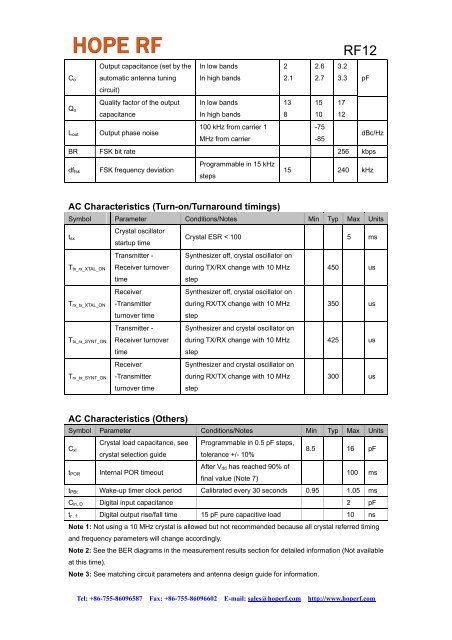
C o<br />
Q o<br />
L out<br />
<strong>RF12</strong><br />
Output capacitance (set by the<br />
automatic antenna tuning<br />
circuit)<br />
In low bands<br />
In high bands<br />
2<br />
2.1<br />
2.6<br />
2.7<br />
3.2<br />
3.3 pF<br />
Quality factor of the output In low bands<br />
13 15 17<br />
capacitance<br />
In high bands<br />
8 10 12<br />
Output phase noise<br />
100 kHz from carrier 1<br />
-75<br />
MHz from carrier<br />
-85<br />
dBc/Hz<br />
BR <strong>FSK</strong> bit rate 256 kbps<br />
df fsk<br />
Programmable in 15 kHz<br />
<strong>FSK</strong> frequency deviation<br />
15 240 kHz<br />
steps<br />
AC Characteristics (Turn-on/Turnaround timings)<br />
Symbol Parameter Conditions/Notes Min Typ Max Units<br />
Crystal oscillator<br />
t sx<br />
Crystal ESR < 100 5 ms<br />
startup time<br />
Transmitter -<br />
T tx_rx_XTAL_ON Receiver turnover<br />
time<br />
Receiver<br />
T rx_tx_XTAL_ON -Transmitter<br />
turnover time<br />
Transmitter -<br />
T tx_rx_SYNT_ON Receiver turnover<br />
time<br />
T rx_tx_SYNT_ON<br />
Receiver<br />
-Transmitter<br />
turnover time<br />
Synthesizer off, crystal oscillator on<br />
during TX/RX change with 10 MHz<br />
step<br />
Synthesizer off, crystal oscillator on<br />
during RX/TX change with 10 MHz<br />
step<br />
Synthesizer and crystal oscillator on<br />
during TX/RX change with 10 MHz<br />
step<br />
Synthesizer and crystal oscillator on<br />
during RX/TX change with 10 MHz<br />
step<br />
450 us<br />
350 us<br />
425 us<br />
300 us<br />
AC Characteristics (Others)<br />
Symbol Parameter Conditions/Notes Min Typ Max Units<br />
C xl<br />
t POR<br />
Crystal load capacitance, see Programmable in 0.5 pF steps,<br />
8.5 16 pF<br />
crystal selection guide<br />
tolerance +/- 10%<br />
After V dd has reached 90% of<br />
Internal POR timeout<br />
100 ms<br />
final value (Note 7)<br />
t PBt Wake-up timer clock period Calibrated every 30 seconds 0.95 1.05 ms<br />
C in, D Digital input capacitance 2 pF<br />
t r , f Digital output rise/fall time 15 pF pure capacitive load 10 ns<br />
Note 1: Not using a 10 MHz crystal is allowed but not recommended because all crystal referred timing<br />
and frequency parameters will change accordingly.<br />
Note 2: See the BER diagrams in the measurement results section for detailed information (Not available<br />
at this time).<br />
Note 3: See matching circuit parameters and antenna design guide for information.<br />
Tel: +86-755-86096587 Fax: +86-755-86096602 E-mail: sales@hoperf.com http://www.hoperf.com