RF12 Universal ISM Band FSK Transceiver
RF12 Universal ISM Band FSK Transceiver
RF12 Universal ISM Band FSK Transceiver

Create successful ePaper yourself
Turn your PDF publications into a flip-book with our unique Google optimized e-Paper software.
<strong>RF12</strong><br />
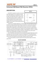
DETAILED FEATURE-LEVEL DESCRIPTION<br />
The <strong>RF12</strong> <strong>FSK</strong> transceiver is designed to cover the unlicensed frequency bands at 315, 433, 868<br />
and 915 MHz. The devices facilitate compliance with FCC and ETSI requirements.<br />
The receiver block employs the Zero-IF approach with I/Q demodulation, allowing the use of a<br />
minimal number of external components in a typical application. The <strong>RF12</strong> incorporates a fully integrated<br />
multi-band PLL synthesizer, PA with antenna tuning, an LNA with switch-able gain, I/Q down converter<br />
mixers, baseband filters and amplifiers, and an I/Q demodulator followed by a data filter.<br />
PLL<br />
The programmable PLL synthesizer determines the operating frequency, while preserving accuracy<br />
based on the on-chip crystal-controlled reference oscillator. The PLL’s high resolution allows the usage of<br />
multiple channels in any of the bands.<br />
The RF VCO in the PLL performs automatic calibration, which requires only a few microseconds.<br />
Calibration always occurs when the synthesizer starts. If temperature or supply voltage changes<br />
significantly, VCO recalibration can be invoked easily. Recalibration can be initiated at any time by<br />
switching the synthesizer off and back on again.<br />
RF Power Amplifier (PA)<br />
The power amplifier has an open-collector differential output and can directly drive a loop antenna<br />
with a programmable output power level. An automatic antenna tuning circuit is built in to avoid costly<br />
trimming procedures and the so-called “hand effect.”<br />
LNA<br />
The LNA has 250 Ohm input impedance, which functions well with the proposed antennas. If the<br />
RF input of the chip is connected to 50 Ohm devices, an external matching circuit is required to provide<br />
the correct matching and to minimize the noise figure of the receiver.<br />
The LNA gain can be selected (0, –6, –14, –20 dB relative to the highest gain) according to RF signal<br />
strength. It can be useful in an environment with strong interferers.<br />
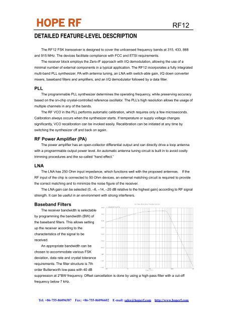
Baseband Filters<br />
The receiver bandwidth is selectable<br />
by programming the bandwidth ( BW) of<br />
the baseband filters. This allows setting<br />
up the receiver according to the<br />
characteristics of the signal to be<br />
received.<br />
An appropriate bandwidth can be<br />
chosen to accommodate various <strong>FSK</strong><br />
deviation, data rate and crystal tolerance<br />
requirements. The filter structure is 7th<br />
order Butterworth low-pass with 40 dB<br />
suppression at 2*BW frequency. Offset cancellation is done by using a high-pass filter with a cut-off<br />
frequency below 7 kHz.<br />
Tel: +86-755-86096587 Fax: +86-755-86096602 E-mail: sales@hoperf.com http://www.hoperf.com