Xilinx - Design Reuse Methodology for ASIC and FPGA Designers.pdf
Xilinx - Design Reuse Methodology for ASIC and FPGA Designers.pdf
Xilinx - Design Reuse Methodology for ASIC and FPGA Designers.pdf

Create successful ePaper yourself
Turn your PDF publications into a flip-book with our unique Google optimized e-Paper software.
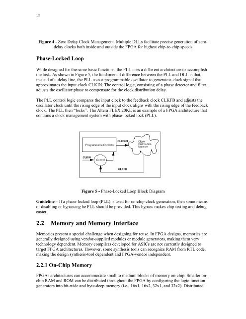
12Figure 4 - Zero Delay Clock Management. Multiple DLLs facilitate precise generation of zerodelayclocks both inside <strong>and</strong> outside the <strong>FPGA</strong> <strong>for</strong> highest chip-to-chip speedsPhase-Locked LoopWhile designed <strong>for</strong> the same basic functions, the PLL uses a different architecture to accomplishthe task. As shown in Figure 5, the fundamental difference between the PLL <strong>and</strong> DLL is that,instead of a delay line, the PLL uses a programmable oscillator to generate a clock signal thatapproximates the input clock CLKIN. The control logic, consisting of a phase detector <strong>and</strong> filter,adjusts the oscillator phase to compensate <strong>for</strong> the clock distribution delay.The PLL control logic compares the input clock to the feedback clock CLKFB <strong>and</strong> adjusts theoscillator clock until the rising edge of the input clock aligns with the rising edge of the feedbackclock. The PLL then “locks”. The Altera FLEX 20KE is an example of a <strong>FPGA</strong> architecture thatcontains a clock management system with phase-locked lock (PLL).Figure 5 - Phase-Locked Loop Block DiagramGuideline – If a phase-locked loop (PLL) is used <strong>for</strong> on-chip clock generation, then some meansof disabling or bypassing he PLL should be provided. This bypass makes chip testing <strong>and</strong> debugeasier.2.2 Memory <strong>and</strong> Memory InterfaceMemories present a special challenge when designing <strong>for</strong> reuse. In <strong>FPGA</strong> designs, memories aregenerally designed using vendor-supplied modules or module generators, making them verytechnology dependent. Memory compilers developed <strong>for</strong> <strong>ASIC</strong>s are not currently designed totarget <strong>FPGA</strong> architectures. However, some synthesis tools can recognize RAM from RTL code,making the design synthesis-tool dependent <strong>and</strong> <strong>FPGA</strong>-vendor independent.2.2.1 On-Chip Memory<strong>FPGA</strong>s architectures can accommodate small to medium blocks of memory on-chip. Smaller onchipRAM <strong>and</strong> ROM can be distributed throughout the <strong>FPGA</strong> by configuring the logic functiongenerators into bit-wide <strong>and</strong> byte-deep memory (i.e., 16x1, 16x2, 32x1, <strong>and</strong> 32x2). Distributed