
You also want an ePaper? Increase the reach of your titles
YUMPU automatically turns print PDFs into web optimized ePapers that Google loves.
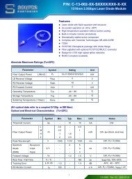
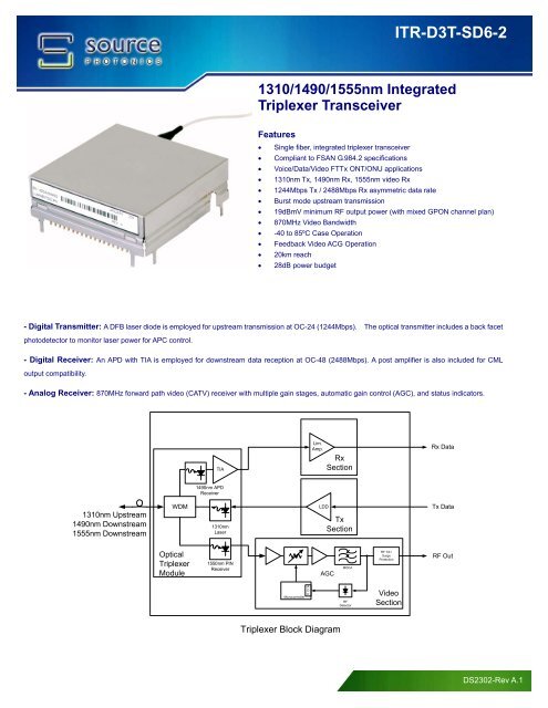
ITR-D3T-SD6-21310/1490/1555nm IntegratedTriplexer TransceiverFeatures• Single fiber, integrated triplexer transceiver• Compliant to FSAN G.984.2 specifications• Voice/Data/Video FTTx ONT/ONU applications• 1310nm Tx, 1490nm Rx, 1555nm video Rx• 1244Mbps Tx / 2488Mbps Rx asymmetric data rate• Burst mode upstream transmission• 19dBmV minimum RF output power (with mixed GPON channel plan)• 870MHz Video Bandwidth• -40 to 85ºC Case Operation• Feedback Video ACG Operation• 20km reach• 28dB power budget- Digital Transmitter: A DFB laser diode is employed for upstream transmission at OC-24 (1244Mbps). The optical transmitter includes a back facetphotodetector to monitor laser power for APC control.- Digital Receiver: An APD with TIA is employed for downstream data reception at OC-48 (2488Mbps). A post amplifier is also included for CMLoutput compatibility.- Analog Receiver: 870MHz forward path video (CATV) receiver with multiple gain stages, automatic gain control (AGC), and status indicators.TIALim.Amp.RxSectionRx Data1490nm APDReceiver1310nm Upstream1490nm Downstream1555nm DownstreamWDM1310nmLaserLDDTxSectionTx DataOpticalTriplexerModule1550nm PINReceiverAGCMOCARF Tilt /SurgeProtectionRF OutADCMicrocontrollerRFDetectorVideoSectionTriplexer Block DiagramDS2302-Rev A.1
ITR-D3T-SD6-2Absolute Maximum RatingsUsage of this transceiver shall adhere to the following absolute maximum ratings. Stresses beyond those in Table 1 may cause permanent damage tothe unit. These are stress ratings only, and functional operation of the unit at these or any other conditions beyond those indicated in the operationalsections of the specifications is not implied. Exposure to absolute maximum rating conditions for extended periods may affect unit reliability.Table 1 - Absolute Maximum RatingsParameter Minimum Maximum Unit/ConditionsAmbient Storage Temperature -40 85 ºCOperating Case Temperature -40 85 ºCOperating Case Humidity Range 10% 90% non-condensingESD Sensitivity (Human Body Model) - 1000 VLead Soldering Temperature - 260ºC 10 secVdd_+12V - 15 VVcc_Rx -0.4 +4.2 VVcc_Tx -0.4 Vcc_Rx + 1 VVcc_µC -0.4 +4.2 VModule CharacteristicsTable 2 - Module CharacteristicsParameter Minimum Typical Maximum Unit/Conditions1555nm external to 1490 nm Rx Isolation 32 - - dB1490nm external to 1555nm Rx Isolation 32 - - dB1310nm external to 1555nm Video Isolation 40 - - dB1310nm external to 1490nm data Isolation 30 - - dB1310nm Tx to 1490nm Rx Optical Crosstalk - - -47 dB1310nm Tx to 1555nm Rx Optical Crosstalk - - -47 dBBack Reflection @ 1310nm - - -6 dBBack Reflection @ 1555nm - - -32 dBBack Reflection @ 1490nm - - -20 dBTotal 3.3V Supply Current - - 350 mATotal 12V Supply Current - - 225 mAPSRR (Power Supply Rejection) - - 100 mVp-pDS2302-Rev A.1
ITR-D3T-SD6-2Table 5 – Video Receiver SpecificationsParameter Minimum Typical Maximum Unit Notes12V Operating Voltage Range 11.7 - 13.2 VFrequency Range 54 - 870 MHzReceiver Wavelength (Bandwidth) 1550 1555 1560 nmResponsivity 0.8 - - A/WAnalog Channels 40 - - OMI = 4.3%/channelDigital Channels 63 - - OMI = 2.15%/channelChannel Bandwidth - 4 - MHzChannel Spacing - 6 - MHzVideo PD Monitor Accuracy - - 5 %AGC Time Constant 0.5 - - sReceived Average Optical Power -8 - 2 dBmRF Channel Output Power 55 MHz a 19 - 23 dBmVRF Channel Output Power 450 MHz a 19.5 - 23.5 dBmVRF Channel Output Power 870 MHz a,b 15 - 22 dBmVS22 Output Return Loss 14 20 - dB 75ΩDistortionsCSOCTB---65-62-55-55dBcFor digital channels, CSO max anCTB max will be 7 dB higherCarrier to Noise Ratio (CNR) 46 - - dBa) Valid with CW carriers with Register 32 = 00b) 6 dB lower because these are digital channel frequenciesDS2302-Rev A.1
ITR-D3T-SD6-2Table 6 – Suggested Start-up SequenceStepAction1 Power up the host system, with the RESET pin pulled to ground via a
ITR-D3T-SD6-2Pin DefinitionsRefer to Table 7 for a description of the function of each I/O pin.Table 7 - Module Pin DefinitionsPin Number Label Definition1 GND_A Common ground2 GND_Rx Digital Rx ground3 Vcc_Rx Digital Rx Vcc4 SDSignal Detect output. LVTTL with internal 3.3kΩ pull-up. Asserts HIGH when input optical signal levelis above threshold.5 RXD+ RX data output, CML. 50Ω terminated to Vcc and AC coupled to module output (0.1μF)6 RXD- RX data bar output, CML. 50Ω terminated to Vcc and AC coupled to module output (0.1μF)7 BEN+ Burst Enable input, internally DC coupled.8 BEN- Burst Enable bar input, internally DC coupled.9 GND_Tx Digital Tx ground10 TXD+ Tx data input, CML. Internally DC coupled. 100Ω differential termination.11 GND_Tx Digital Tx ground12 TXD- Tx data bar input, CML. Internally DC coupled. 100Ω differential termination.13 Vcc_Tx Digital Tx Vcc14 SDA I 2 C Data input/output. LVTTL15 SCL I 2 C Clock input. LVTTL16 INT Interrupt output. LVTTL with internal 100kΩ pull-up. Active LOW.17 Vdd_+12V Video Rx 12V Vdd18 Vcc_3.3V Microcontroller Vcc19 Reset Reset input. LVTTL. Internal pull up. Active low.20 GND_A Common ground21 RF_GND RF ground22 RF_SIGNAL RF signal23 RF_GND RF groundDS2302-Rev A.1
ITR-D3T-SD6-2Package Diagram23.5 ± 1.5[597 ± 38]Bottom ViewNotes1. Dimensions in inches [mm]2. Minimum fiber bend radius = 1.18 [30.00]Bottom ViewDS2302-Rev A.1
ITR-D3T-SD6-2Ordering InformationTable 8 - Ordering InformationITx - xyz - xy z - x - xx Application Type x PON Standard y Tx Rate z Rx Rate xy Customer z Platform Revision SupplementalRIntegrated Triplexer,Residential ApplicationBBPON, Class B, SC/APCpigtail1 155Mbps T 2x Tx rate SD Standard 1μC based; SMBRF connectorNumericvalueCCommercial temp.range (0-70C)CIntegrated Triplexer, CurbApplicationCBPON, Class B, SCreceptacle2 622Mbps F 4x xyCustomerspecific2μC based; 3-pinRF connectorDIntegrated Triplexer, DigitalOnlyGGPON, 25dB budget,SC/APC pigtail3 1244Mbps E 8x 3μC based; SMB;BPON gainVIntegrated Triplexer, VideoOnlyHGPON, 28dB Budget,SC/APC Pigtail(FP Laser)4 2488Mbps S 16x 5μC based; SMB;HIGH gainDGPON, 28dB Budget,SC/APC Pigtail(DFB Laser)5 4800Mbps 6μC based; 3RF;HIGH gain7μC based; SMB;Next gen.8μC based; 3RF;Next gen.Table 12 - Device Handling/ESD ProtectionThe devices are static sensitive and may easily be damaged if care is not taken during handling. The following handling practices arerecommended.1 Devices should be handled on benches with conductive and grounding surfaces.2 All personnel, test equipment and tools shall be grounded.3 Do not handle the devices by their leads.4 Store devices in protective foam or carriers.5 Avoid the use of non-conductive plastics, rubber, or silk in the area where the devices are handled6 All modules shall be packaged in materials that are anti-static to protect against adverse electrical environments.Avoid applications of any voltage higher than maximum rated voltages to this part. For proper operation, any VIN or VOUT should be7constrained to the range GND ≤ (VIN or VOUT) ≤ VCC. Unused inputs must always be tied to an appropriate logic voltage (e.g.either GND or VCC). Unused outputs must be left open.DS2302-Rev A.1
ITR-D3T-SD6-2WarningsHandling Precautions: This device is susceptible to damage as a result of electrostatic discharge (ESD). A static free environment is highlyrecommended. Follow guidelines according to proper ESD procedures.Laser Safety: Radiation emitted by laser devices can be dangerous to human eyes. Avoid eye exposure to direct or indirect radiation.Legal NoticeIMPORTANT NOTICE!All information contained in this document is subject to change without notice, at <strong>Source</strong> <strong>Photonics</strong>’ sole and absolute discretion. <strong>Source</strong> <strong>Photonics</strong>warrants performance of its products to current specifications only in accordance with the company’s standard one-year warranty; however, specificationsdesignated as “preliminary” are given to describe components only, and <strong>Source</strong> <strong>Photonics</strong> expressly disclaims any and all warranties for said products,including express, implied, and statutory warranties, warranties of merchantability, fitness for a particular purpose, and non-infringement of proprietaryrights. Please refer to the company’s Terms and Conditions of Sale for further warranty information.<strong>Source</strong> <strong>Photonics</strong> assumes no liability for applications assistance, customer product design, software performance, or infringement of patents, services,or intellectual property described herein. No license, either express or implied, is granted under any patent right, copyright, or intellectual property right,and <strong>Source</strong> <strong>Photonics</strong> makes no representations or warranties that the product(s) described herein are free from patent, copyright, or intellectual propertyrights. Products described in this document are NOT intended for use in implantation or other life support applications where malfunction may result ininjury or death to persons. <strong>Source</strong> <strong>Photonics</strong> customers using or selling products for use in such applications do so at their own risk and agree to fullydefend and indemnify <strong>Source</strong> <strong>Photonics</strong> for any damages resulting from such use or sale.© Copyright <strong>Source</strong> <strong>Photonics</strong>, Inc. 2007~2008All Rights Reserved.All information contained in this document is subject to change without notice. The products described in this document are NOTintended for use in implantation or other life support applications where malfunction may result in injury or death to persons.The information contained in this document does not affect or change <strong>Source</strong> <strong>Photonics</strong> product specifications or warranties. Nothing inthis document shall operate as an express or implied license or indemnity under the intellectual property rights of <strong>Source</strong> <strong>Photonics</strong> orthird parties. All information contained in this document was obtained in specific environments, and is presented as an illustration. Theresults obtained in other operating environments may vary.THE INFORMATION CONTAINED IN THIS DOCUMENT IS PROVIDED ON AN ”AS IS” BASIS. In no event will <strong>Source</strong> <strong>Photonics</strong> beliable for damages arising directly from any use of the information contained in this document.ContactSOURCE PHOTONICS20550 NORDHOFF ST.CHATSWORTH, CA 91311sales@sourcephotonics.comTel: 818-773-9044 Fax: 818-576-9486Or visit our website: http://www.sourcephotonics.comDS2302-Rev A.1