TigerSHARC DSP Hardware Specification, Revision 1.0.2, Link Ports
TigerSHARC DSP Hardware Specification, Revision 1.0.2, Link Ports
TigerSHARC DSP Hardware Specification, Revision 1.0.2, Link Ports

Create successful ePaper yourself
Turn your PDF publications into a flip-book with our unique Google optimized e-Paper software.
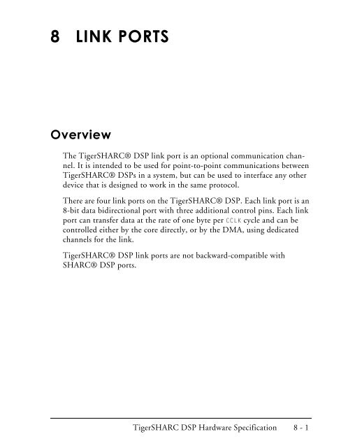
8 LINK PORTSFigure 8-0.Table 8-0.Listing 8-0.OverviewThe <strong>TigerSHARC</strong>® <strong>DSP</strong> link port is an optional communication channel.It is intended to be used for point-to-point communications between<strong>TigerSHARC</strong>® <strong>DSP</strong>s in a system, but can be used to interface any otherdevice that is designed to work in the same protocol.There are four link ports on the <strong>TigerSHARC</strong>® <strong>DSP</strong>. Each link port is an8-bit data bidirectional port with three additional control pins. Each linkport can transfer data at the rate of one byte per CCLK cycle and can becontrolled either by the core directly, or by the DMA, using dedicatedchannels for the link.<strong>TigerSHARC</strong>® <strong>DSP</strong> link ports are not backward-compatible withSHARC® <strong>DSP</strong> ports.<strong>TigerSHARC</strong> <strong>DSP</strong> <strong>Hardware</strong> <strong>Specification</strong> 8 - 1
<strong>Link</strong> Architecture<strong>Link</strong> ArchitectureThe link port has two parts—transmitter and receiver. Each has a doublebuffer, as shown in Figure 8-1 on page 8-2. The Tx and Rx registers arememory-mapped Uregs. The shift registers are not accessible by software.All are 128-bit registers.Internal BusTx -Transmitter BufferRx -Receiver BufferTransmitterShift RegisterReceiverShift Register<strong>Link</strong> PortFigure 8-1. <strong>Link</strong> Port Architecture8 - 2 <strong>TigerSHARC</strong> <strong>DSP</strong> <strong>Hardware</strong> <strong>Specification</strong>
<strong>Link</strong> Architecturefrom the shift register to the Rx register. When the shift register is freeagain it can enable receiving data again.Table 8-2. <strong>Link</strong> Port RegisterGroup 0x25 Reg #RegisterQuads<strong>Link</strong>s 0-3 RegistersDirect MemAddressRemarksReg 0x0 - 3 LBUFTX0 <strong>Link</strong> # 0 Tx register 0x1804A0-3 -Reg 0x4 - 7 LBUFRX0 <strong>Link</strong> # 0 Rx register 0x1804A4-7 Read onlyReg 0x8 - B LBUFTX1 <strong>Link</strong> # 1 Tx register 0x1804A8-BReg 0xC - F LBUFRX1 <strong>Link</strong> # 1 Rx register 0x1804AC-F Read onlyReg 0x10 - 13 LBUFTX2 <strong>Link</strong> # 2 Tx register 0x1804B0-3 –Reg 0x14 - 17 LBUFRX2 <strong>Link</strong> # 2 Rx register 0x1804B4-7 Read onlyReg 0x18 - 1B LBUFTX3 <strong>Link</strong> # 3 Tx register 0x1804B8-B –Reg 0x1C - 1F LBUFRX3 <strong>Link</strong> # 3 Rx register 0x1804BC-F Read onlyGroup 0x27 Reg #RegisterQuadsReserved for <strong>Link</strong>s 4-5Registers and ControlRegistersDirect MemAddressRemarksReg 0x0 LCTL0 <strong>Link</strong> # 0 control register 0x1804E0 Reset value:0x400(LREN=1)Reg 0x1 LCTL1 <strong>Link</strong> # 1 control register 0x1804E1 Reset value:0x400(LREN=1)8 - 4 <strong>TigerSHARC</strong> <strong>DSP</strong> <strong>Hardware</strong> <strong>Specification</strong>
<strong>Link</strong> <strong>Ports</strong>Table 8-2. <strong>Link</strong> Port Register (Continued)Reg 0x2 LCTL2 <strong>Link</strong> # 2 control register 0x1804E2 Reset value:0x400(LREN=1)Reg 0x3 LCTL3 <strong>Link</strong> # 3 control register 0x1804E3 Reset value:0x400(LREN=1)Reg 0x10 LSTAT0 <strong>Link</strong> # 0 status register 0x1804F0 Read onlyReg 0x11 LSTAT1 <strong>Link</strong> # 1 status register 0x1804F1 Read onlyReg 0x12 LSTAT2 <strong>Link</strong> # 2 status register 0x1804F2 Read onlyReg 0x13 LSTAT3 <strong>Link</strong> # 3 status register 0x1804F3 Read onlyReg 0x18 LSTATC0 <strong>Link</strong> # 0 status clear registerReg 0x19 LSTATC1 <strong>Link</strong> # 1 status clear registerReg 0x1A LSTATC2 <strong>Link</strong> # 2 status clear registerReg 0x1B LSTATC3 <strong>Link</strong> # 3 status clear register0x1804F80x1804F90x1804FA0x1804FBRead onlyRead onlyRead onlyRead onlyDMAEach link port is associated with two DMA channels. One channel is usedfor transmitting data while the other is used for receiving data. The twoDMA channels can interface with either internal or external memory.<strong>TigerSHARC</strong> <strong>DSP</strong> <strong>Hardware</strong> <strong>Specification</strong> 8 - 5
<strong>Link</strong> <strong>Ports</strong>The interrupt can be used for either of two purposes:• As an error indication when the system designer intends to managethe data by using the DMA.• For control indication between different <strong>TigerSHARC</strong>® <strong>DSP</strong>s.The link interrupt routine can read the link receiver buffer, analyzeit, and behave accordingly. For more information, see “<strong>Link</strong> PortDMA Control” on page 7-22.Reset and BootThe link ports can also be used for boot. After reset, all the link ports areinitialized to receive mode. The link receive DMA channel is initialized toreceive 256 words and write them to internal memory block 0, address 0.For more information, see “Boot <strong>Link</strong> to Internal Memory” on page 7-70.The DMA channel of any port not being used for boot must be clearedand re-initialized. If the DMA channel is not deactivated, the link interruptmechanism will not work. The link may be re-initialized as well.If both links that are connected to each other start transmitting atthe same time, unexpected results may occur (up to protocol deadlock).The system designer must initialize the system in such a waythat one of the links transmits first.<strong>Link</strong> Port Communication ProtocolThe link port communicates through an 8-bit data bus, using three controlsignals. There are four sets of link pins. In the link pin names, the “x”<strong>TigerSHARC</strong> <strong>DSP</strong> <strong>Hardware</strong> <strong>Specification</strong> 8 - 7
<strong>Link</strong> Port Communication Protocolstands for the link pin set—0, 1, 2 or 3. The control signal pins are asfollows:• LxCLKIN and LxCLKOUT – Clock/acknowledge input and output pinsThe LxCLKIN pin is an input that functions as a clock when the linkreceives, and as acknowledge when the link transmits. The LxCLKOUTpin is an output that functions as a clock when the link transmits,and as acknowledge when the link receives.• LxDAT [7:0] – Data bus input and outputThe data are transmitted or received one byte every LxCLK edge.Transfers are of quad words. The transfer begins from byte 0.• LxDIR – <strong>Link</strong> direction indicationThe LxDIR pin is an output that indicates if the link is transmittingor receiving. It is used when the links are buffered. (For example, bydifferential low swing buffers for long twisted-pair wires).LxCLKINLxCLKOUTLxDAT8LxCLKINLxCLKOUTLxDATFigure 8-2. Minimal <strong>Link</strong> Configuration – No Buffering8 - 8 <strong>TigerSHARC</strong> <strong>DSP</strong> <strong>Hardware</strong> <strong>Specification</strong>
<strong>Link</strong> <strong>Ports</strong>3. One cycle after the transmission starts, the receiver drives the transmitter’sLxCLKIN low for a connectivity check. The LxCLKIN will remain low if itcan not receive another quad word following the current one. In this case,the LxCLKIN is set back after the buffer is free. If the buffer is empty, thereceiver will set LxCLKIN high.The LxCLKOUT is used as the synchronization clock, driven by the transmitter.Data are latched in the receive buffer on the falling and rising edges ofLxCLKOUT.connectivitychecknext transferacknowledgenext transferbeginsLxCLKOUTLxCLKINLxDAT [7:0]b0 b1 b2 b3 b4 b5b15 ver — b0 b1Figure 8-5. Quad-word Completion and a New Quad-word BeginningWhen Vere Bit is SetThe completion of the transfer and beginning of a new transfer can bedone according to one of two scenarios, according to the VERE bit in theLCTLx register (enable verification). If the VERE bit is set, the checksumbyte is sent after the last byte in quad word, on the rising edge. In thiscase, the falling edge data are meaningless and the checksum byte is sam-<strong>TigerSHARC</strong> <strong>DSP</strong> <strong>Hardware</strong> <strong>Specification</strong> 8 - 11
<strong>Link</strong> Port Communication Protocolpled at the LxCKIN rising edge. If the VERE bit is cleared, the first byte ofthe next quad word follows the last byte of the current word.connectivitychecknext transferacknowledgenext transferbeginsLxCLKOUTLxCLKINLxDAT [7:0]b0 b1 b2 b3 b4 b5b13 b14 b15 b0 b1Figure 8-6. Quad word Completion and a New Quad word BeginningWhen Vere Bit is ClearedThe LxCLKIN, driven by the receiver to the transmitter, is always used as a‘wait’ indication and sometimes used as a connectivity check to ensurethat the receiver is receiving the current transmission.When used as a wait indicator, LxCLKIN is driven low. If LxCLKIN stays low,the transmitter can complete the current quad word, but it can not begin anew quad word transmission. If there are more data to be transmitted, thetransmitter sets the LxCLKOUT to low and waits until LxCLKIN is driven highby the receiver.If LxCLKIN is set high before the 12th edge, there will be back-to-backtransmissions.8 - 12 <strong>TigerSHARC</strong> <strong>DSP</strong> <strong>Hardware</strong> <strong>Specification</strong>
<strong>Link</strong> Port Communication ProtocolThe token is switched if LxCLKOUT remains high long enough, thus indicatingthe former transmitter (A in this example) did not regret the tokenswitch and can receive data. (Refer to the Data Sheet.)data are transmitted by Adata are transmitted by BLxCLKOUTtoken requestLxCLKINLxDAT [7:0]a14a15b0 b1 b2 b3LxDIR (A)LxDIR (B)Figure 8-8. Token Switch from A to BThe link has an output LxDIR that indicates the data direction. WhenLxDIR is high, the link data pins direction is output. LxDIR is cleared whenthe transmitter enables a token switch. LxDIR is set after the token switch,when the data are transmitted—the high value does not overlap. This controlcan be used by any type of bidirectional buffers on the data lines.The former transmitter can regret the token switch if it gets more data totransmit after a pause, and if the former receiver has not yet requested atoken switch.8 - 14 <strong>TigerSHARC</strong> <strong>DSP</strong> <strong>Hardware</strong> <strong>Specification</strong>
<strong>Link</strong> <strong>Ports</strong>A enables token switchA regrets token switchacknowledgeA starts transmittingLxCLKOUTtoken switch enableLxCLKINLxDAT [7:0]a14a15a0 a1 a2 a3LxDIR (A)LxDIR (B)Figure 8-9. Transmitter Regrets a Token SwitchThe former transmitter must keep the LxCLKOUT high long enough to guaranteethat the token switch takes place. (See Data Sheet.) The receivermust request the token switch when it senses its LxCLKIN is high. If thereceiver does not request the token switch in time and the transmitter hasmore data to send, the transmitter indicates that it regrets the token switchby setting LxCLKOUT low (token request), which cancels the token switch<strong>TigerSHARC</strong> <strong>DSP</strong> <strong>Hardware</strong> <strong>Specification</strong> 8 - 15
Transmission DelaysAn example of a token switch regret is shown in Figure 8-9 on page 8-15.In this example:1. After the transmitter has set LxCLKOUT high, the receiver identifiesthis as token switch enable and requests the token switch.2. The receiver’s request is too late to guarantee the token switch andthe transmitter signals a regret by setting LxCLKOUT low. Thereceiver identifies this and goes back to being a receiver. Thereceiver indicates that it is ready to receive more data by ackowledging.The transmitter starts transmitting again.3. The LxDIR pin of the transmitter changes to low when it enablesthe token switch. The transmitter sets it LxDIR back to high onlywhen the transmitter starts to transmit data again. The receiverdoes not set its LxDIR output high because it never gets to the pointof transmitting data.Transmission DelaysThe links should be able to function even if there are delays between thesource and destination. The delays of the different link signals (LxCLK andLxDAT) are matched to tolerances specified in the data sheet.The data sampled at the receiver uses the input LxCLK, so the delay has noeffect. Complications can arise, however, when token switches areinvolved. The maximum delay can be derived from information providedin the Data Sheet.8 - 16 <strong>TigerSHARC</strong> <strong>DSP</strong> <strong>Hardware</strong> <strong>Specification</strong>
<strong>Link</strong> <strong>Ports</strong>data are transmitted by Adata are transmitted by BTiming at ALxCLKOUTLxCLKINtransmission delayLxDAT [7:0]a14a15b0b1b2Lx DIR (A)Timing at BLxCLKINLxCLKOUTLxDAT [7:0]a12a13a14a15b0 b1 b2 b3LxDIR (B)Figure 8-10. Token Switch from A to B with DelayFigure 8-10 shows the effect of the delay between two <strong>TigerSHARC</strong>®<strong>DSP</strong>s. The transmitter (<strong>TigerSHARC</strong>® <strong>DSP</strong> A) sets LxCLKOUT high toindicate a token switch enable. The receiver (<strong>TigerSHARC</strong>® <strong>DSP</strong> B)<strong>TigerSHARC</strong> <strong>DSP</strong> <strong>Hardware</strong> <strong>Specification</strong> 8 - 17
Error Detection Mechanismssenses this after a delay. The receiver then sets its LxCLKOUT (which isLxCLKIN of the transmitter) low, and waits to see if the transmitter regretsthe token switch. The token switch will take place if the transmitter hasnot regretted the token switch. Refer to the Data Sheet for specific timingdata.Error Detection MechanismsThe link ports support on-the-fly error checks. When the link detects anerror condition, it operates in the following sequence:1. The TER or RER field in LSTATx is set according to the error type.2. If the TTOE (Transmit Time Out check Enable), CERE (ConnectivityError check Enable), and RTOE (Receive Time Out check Enable)bits are set in the LCTLx registers, a hardware error interrupt is set.(See “<strong>Hardware</strong> Error Operations” on page 5-8.)3. If the VERE (checksum Verification Error Enable) is set in the LCTLxregisters, the RER field in LSTSx is set according to this error typeand a hardware error interrupt is set. (See “<strong>Hardware</strong> Error Operations”on page 5-8.)4. The link is stuck until the error status is read (from the LSTATCx).After reading the status from the destructive address, it should be re-initializedto start working.8 - 18 <strong>TigerSHARC</strong> <strong>DSP</strong> <strong>Hardware</strong> <strong>Specification</strong>
<strong>Link</strong> <strong>Ports</strong>Transmitter Error DetectionTwo kind of transmitter errors are detected:1. Connectivity checkThe transmitter checks the LxCLKIN pin on every quad transmission.That pin acts as the acknowledge signal. If the acknowledgesignal is not de-asserted for a minimum time period during thetransmission, an error has occurred: the TER[0] bit is set in theLSTATx register and a hardware interrupt is issued. Refer to theData Sheet for specific timing data.2. Time OutIf the transmitter’s acknowledge signal (LxCLKIN) is de-asserted fora time period of 2048 clock cycles, and the transmitter has data totransmit, an error has occurred: the TER[1] bit is set in the LSTATxregister and a hardware interrupt is issued.Receiver Error DetectionTwo kind of receiver errors are detected:1. ChecksumThe transmitter creates and sends for a special Verification byte onevery transmitted quad word (if it is enabled). This byte is a checksumcalculation product of all data bytes that have beentransmitted. It is sent at the end of every 16-byte (quad word)transmission. The receiver compares the transmitted Verificationbyte to the local Verification byte created during data reception. Ifthe two bytes differ the RER[0] bit is set in the LSTATx register and ahardware interrupt is issued.<strong>TigerSHARC</strong> <strong>DSP</strong> <strong>Hardware</strong> <strong>Specification</strong> 8 - 19
Control Register (LCTLx)The checksum algorithm is:Checksum = B0 + B1 + … + B15 + C0 +C1 + … + C14where:B0, B1, etc. are byte1, byte2 …C0 is the Carry_out from B0 + B1,C1 is the Carry_out from B0 + B1 + B2 + C0,etc.C14 (the Carry_out from B0 + B1 + … + B15 + C0 + C1 + … + C13)is not added to the checksum.2. Time OutIf LxCLKIN is sampled low for a period of 256 cycles, a timeouterror has occurred. The RER[1] bit is set in the LSTATx register anda hardware interrupt is issued.If less than 16 bytes are received and LxCLKIN remains high for morethan four LxCLK cycles, the receiver does not detect a timeout error.The next quad word received overwrites the data in the receivebuffer.Control Register (LCTLx)The Control register programs every link port and contains control bitsunique to each one. There are four control registers—one for each linkport. The register is read/write.8 - 20 <strong>TigerSHARC</strong> <strong>DSP</strong> <strong>Hardware</strong> <strong>Specification</strong>
<strong>Link</strong> <strong>Ports</strong>LCTLx Register format76 5:3210PSIZELTENSPDVEREReserved31:12111098ReservedRTOELRENCERETTOETable 8-3. LCTLx Register Bit DescriptionsBit # Bit Description1:0 Reserved2 VERE Verification Enable5:3 SPD Transfer SpeedEnables checksum verification for received data, and creationof checksum on data transmission. Clear after reset.Defines the communication rate in which bytes are transmitted/received:1000… CCLK/8001… CCLK/4010… CCLK/3011… CCLK/21XX…ReservedThis field is clear after reset.6 LTEN Transmit EnableWhen cleared, any on-going transmit procedure inside theblock is ceased immediately, data are tri-stated. Any data thathave been written to the transmitter register before clearingLTEN, are cleared, and when setting LTEN again, the Transmitregister will be empty.Upon reset this bit is cleared.<strong>TigerSHARC</strong> <strong>DSP</strong> <strong>Hardware</strong> <strong>Specification</strong> 8 - 21
Control Register (LCTLx)Table 8-3. LCTLx Register Bit Descriptions (Continued)Bit # Bit Description7 PSIZE Packet Size—when a packet is completed, the transmitterenables token switch.0… 64 quads in one packet1… Indefinite number of bytes on one packetUpon reset this field is cleared.8 TTOE Transmit Time Out check EnableEnables hardware error interrupt on time out check for transmitteddata.When set, a hardware error interrupt is issued.Upon reset this bit is cleared.9 CERE Connectivity Error check EnableEnables hardware error interrupt on connectivity check errorto transmit link port.When set, a hardware error interrupt is issued.Upon reset this bit is cleared.10 LREN Receive/EnableWhen disabled, any on-going receive procedure inside theblock is ceased immediately and any received data are cleared.When set, the receive register is empty.Upon reset this bit is set.11 RTOE Receive Time Out check Enable31:12 ReservedEnables hardware error interrupt on time out check forreceived data.When set, a hardware error interrupt is issued.Upon reset this bit is cleared.8 - 22 <strong>TigerSHARC</strong> <strong>DSP</strong> <strong>Hardware</strong> <strong>Specification</strong>
<strong>Link</strong> <strong>Ports</strong>1 Note that both transmitter and receiver have to work at the same clock speed, although the clockdoesn’t need to be fully synchronous.After rest:• The register is initialized to 0x400—receive enable.• Transmit is disabled; packet size is 64 quad words.• Clock division is by 8.• DIR pin is disabled.• Verification is disabled and all error checks are disabled.Status Register (LSTATx)The Status register is read only and holds error and status information forevery link port. There are four Status registers, one for each link port. TheStatus registers are read-only—note however, that a read from a clearaddress will clear the error fields RER and TER. For more details, seeTable 3-22 on page 3-41.LSTATx Register format7:65:43:21:0TSTTERRSTRER31:8RESERVED<strong>TigerSHARC</strong> <strong>DSP</strong> <strong>Hardware</strong> <strong>Specification</strong> 8 - 23
Status Register (LSTATx)Table 8-4. LSTATx Register Bit DescriptionsBit # Bit Description1:0 RER Receive Error:00… No error01… Verification byte error10… Receive timeout11… Both errors3:2 RST Receive Status:5:4 TER Transmit error00… Receiver empty01… Receiver shift register is partly full, Rx buffer is free10… Receiver Rx buffer is full, shift register is empty11… Receiver full00… No error01… Connectivity error10… Transmit timeout11… Both errors7:6 TST Transmit Status31:8 ReservedNote that any error causes hardware error interrupt. Readingthe Status register clears the error and resets the state machinefor a new transfer.00… Transmitter empty01… Transmitter is partly full11… Transmitter full8 - 24 <strong>TigerSHARC</strong> <strong>DSP</strong> <strong>Hardware</strong> <strong>Specification</strong>