M2110 Hardware Reference Manual - MEMSIC
M2110 Hardware Reference Manual - MEMSIC
M2110 Hardware Reference Manual - MEMSIC

You also want an ePaper? Increase the reach of your titles
YUMPU automatically turns print PDFs into web optimized ePapers that Google loves.
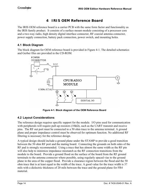
IRIS OEM Edition <strong>Hardware</strong> <strong>Reference</strong> <strong>Manual</strong>4 IRIS OEM <strong>Reference</strong> BoardThe IRIS OEM reference board is a carrier PCB with the same form factor and functionality asthe IRIS family product. It consists of a surface mount module consisting of a processor coreand a two-way radio, high density digital interface connector, RF coaxial antenna connector,power supply connection, battery pack connection, power switch, and mounting holes.4.1 Block DiagramThe block diagram for OEM reference board is provided in Figure 4-1. The detailed schematicsand Gerber files are provided in the CD-ROM.Figure 4-1. Block diagram of the OEM <strong>Reference</strong> Board4.2 Layout ConsiderationsThe reference design requires specific support for the module. I/O pins used for communicationwith peripherals will require pull-up resistors (10kΩ), such as the UART transmit and receivepins. The RF out port must be connected to a 50 ohm trace to the antenna terminal. A groundplane and proper impedance control must be observed for optimum function. No additional RFfiltering is necessary for the reference design.A typical design should include a ground plane under the STAMP to provide a good transitionbetween the 50 ohm RF port and the mating board. Connecting the grounds on both sides of theRF pad is strongly recommended. Using a trace that has almost the same width as the RF pinwill also help to minimize impedance mismatch as the RF connection transitions from themodule to the board. Provide a ground flood on the surface of the board from the RF groundterminals to the antenna connector where possible, using regularly spaced vias to the groundplane in the area of the copper flood. Provide a clearance region between the flood and the 50ohm trace that is at least equal to the width of the trace. A good value for the trace width is 37mils with a dielectric thickness of 20 mils between the trace and the ground plane for FR4material.Page 14Doc. # 7430-0549-01 Rev. A