MAX7219/MAX7221 Serially Interfaced, 8-Digit LED Display Drivers
MAX7219/MAX7221 Serially Interfaced, 8-Digit LED Display Drivers
MAX7219/MAX7221 Serially Interfaced, 8-Digit LED Display Drivers
- No tags were found...

Create successful ePaper yourself
Turn your PDF publications into a flip-book with our unique Google optimized e-Paper software.
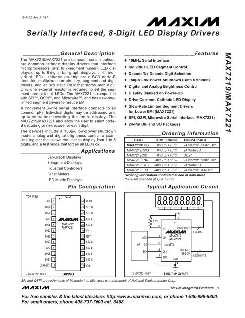
19-4452; Rev 3; 7/97<strong>Serially</strong> <strong>Interfaced</strong>, 8-<strong>Digit</strong> <strong>LED</strong> <strong>Display</strong> <strong>Drivers</strong>_______________General DescriptionThe <strong>MAX7219</strong>/<strong>MAX7221</strong> are compact, serial input/outputcommon-cathode display drivers that interfacemicroprocessors (µPs) to 7-segment numeric <strong>LED</strong> displaysof up to 8 digits, bar-graph displays, or 64 individual<strong>LED</strong>s. Included on-chip are a BCD code-Bdecoder, multiplex scan circuitry, segment and digitdrivers, and an 8x8 static RAM that stores each digit.Only one external resistor is required to set the segmentcurrent for all <strong>LED</strong>s. The <strong>MAX7221</strong> is compatiblewith SPI, QSPI, and Microwire, and has slew-ratelimitedsegment drivers to reduce EMI.A convenient 3-wire serial interface connects to allcommon µPs. Individual digits may be addressed andupdated without rewriting the entire display. The<strong>MAX7219</strong>/<strong>MAX7221</strong> also allow the user to select code-B decoding or no-decode for each digit.The devices include a 150µA low-power shutdownmode, analog and digital brightness control, a scanlimitregister that allows the user to display from 1 to 8digits, and a test mode that forces all <strong>LED</strong>s on.________________________ApplicationsBar-Graph <strong>Display</strong>s7-Segment <strong>Display</strong>sIndustrial ControllersPanel Meters<strong>LED</strong> Matrix <strong>Display</strong>s__________________Pin Configuration____________________________Features♦ 10MHz Serial Interface♦ Individual <strong>LED</strong> Segment Control♦ Decode/No-Decode <strong>Digit</strong> Selection♦ 150µA Low-Power Shutdown (Data Retained)♦ <strong>Digit</strong>al and Analog Brightness Control♦ <strong>Display</strong> Blanked on Power-Up♦ Drive Common-Cathode <strong>LED</strong> <strong>Display</strong>♦ Slew-Rate Limited Segment <strong>Drivers</strong>for Lower EMI (<strong>MAX7221</strong>)♦ SPI, QSPI, Microwire Serial Interface (<strong>MAX7221</strong>)♦ 24-Pin DIP and SO Packages______________Ordering InformationPART<strong>MAX7219</strong>CNG<strong>MAX7219</strong>CWG<strong>MAX7219</strong>C/DTEMP. RANGE0°C to +70°C0°C to +70°C0°C to +70°CPIN-PACKAGE24 Narrow Plastic DIP24 Wide SODice*<strong>MAX7219</strong>ENG -40°C to +85°C 24 Narrow Plastic DIP<strong>MAX7219</strong>EWG<strong>MAX7219</strong>ERG-40°C to +85°C-40°C to +85°C24 Wide SO24 Narrow CERDIPOrdering Information continued at end of data sheet.*Dice are specified at T A = +25°C.________Typical Application Circuit<strong>MAX7219</strong>/<strong>MAX7221</strong>TOP VIEWDIN124DOUTDIG 0223SEG DDIG 4322SEG DP+5VGNDDIG 6DIG 2DIG 3DIG 7GNDDIG 5DIG 1LOAD (CS)456789101112<strong>MAX7219</strong><strong>MAX7221</strong>212019181716151413SEG ESEG CV+ISETSEG GSEG BSEG FSEG ACLKMOSIµP I/OSCK9.53k18112139I SETV+19DIG 0–DIG 7<strong>MAX7219</strong>DIN<strong>MAX7221</strong>LOAD (CS)CLKSEG A–G,SEG DPGNDGND48 DIGITS8 SEGMENTS( ) <strong>MAX7221</strong> ONLYDIP/SO( ) <strong>MAX7221</strong> ONLY 8-DIGIT µP DISPLAYSPI and QSPI are trademarks of Motorola Inc. Microwire is a trademark of National Semiconductor Corp.________________________________________________________________ Maxim Integrated Products 1For free samples & the latest literature: http://www.maxim-ic.com, or phone 1-800-998-8800.For small orders, phone 408-737-7600 ext. 3468.
<strong>Serially</strong> <strong>Interfaced</strong>, 8-<strong>Digit</strong> <strong>LED</strong> <strong>Display</strong> <strong>Drivers</strong><strong>MAX7219</strong>/<strong>MAX7221</strong>ABSOLUTE MAXIMUM RATINGSVoltage (with respect to GND)V+ ............................................................................-0.3V to 6VDIN, CLK, LOAD, CS ...............................................-0.3V to 6VAll Other Pins.............................................-0.3V to (V+ + 0.3V)CurrentDIG0–DIG7 Sink Current................................................500mASEGA–G, DP Source Current.........................................100mAContinuous Power Dissipation (T A = +85°C)Narrow Plastic DIP ..........................................................0.87WWide SO ..........................................................................0.76WNarrow CERDIP.................................................................1.1WStresses beyond those listed under “Absolute Maximum Ratings” may cause permanent damage to the device. These are stress ratings only, and functionaloperation of the device at these or any other conditions beyond those indicated in the operational sections of the specifications is not implied. Exposure toabsolute maximum rating conditions for extended periods may affect device reliability.ELECTRICAL CHARACTERISTICS(V+ = 5V ±10%, R SET = 9.53kΩ ±1%, T A = T MIN to T MAX , unless otherwise noted.)Operating Temperature Ranges<strong>MAX7219</strong>C_G/<strong>MAX7221</strong>C_G ..............................0°C to +70°C<strong>MAX7219</strong>E_G/<strong>MAX7221</strong>E_G ............................-40°C to +85°CStorage Temperature Range .............................-65°C to +160°CLead Temperature (soldering, 10sec) .............................+300°CPARAMETERSYMBOLCONDITIONSMIN TYP MAXUNITSOperating Supply VoltageShutdown Supply CurrentOperating Supply Current<strong>Display</strong> Scan Rate<strong>Digit</strong> Drive Sink CurrentSegment Drive Source CurrentSegment Current Slew Rate(<strong>MAX7221</strong> only)Segment Drive Current Matching<strong>Digit</strong> Drive Leakage(<strong>MAX7221</strong> only)Segment Drive Leakage(<strong>MAX7221</strong> only)<strong>Digit</strong> Drive Source Current(<strong>MAX7219</strong> only)Segment Drive Sink Current(<strong>MAX7219</strong> only)V+I+I+f OSCI DIGITI SEG∆I SEG /∆t∆I SEGI DIGITI SEGI DIGITI SEGAll digital inputs at V+ or GND, T A = +25°CR SET = open circuitAll segments and decimal point on,I SEG_ = -40mA8 digits scannedV+ = 5V, V OUT = 0.65VT A = +25°C, V+ = 5V, V OUT = (V+ - 1V)T A = +25°C, V+ = 5V, V OUT = (V+ - 1V)<strong>Digit</strong> off, V DIGIT = V+4.0 5.53303.01508500 800 1300320-30 -40 -4510 20 50-10VµAmAHzmAmAmA/µsSegment off, V SEG = 0V 1 µA<strong>Digit</strong> off, V DIGIT = (V+ - 0.3V)Segment off, V SEG = 0.3V-25%µAmAmA2 _______________________________________________________________________________________
<strong>Serially</strong> <strong>Interfaced</strong>, 8-<strong>Digit</strong> <strong>LED</strong> <strong>Display</strong> <strong>Drivers</strong>ELECTRICAL CHARACTERISTICS (continued)(V+ = 5V ±10%, R SET =9.53kΩ ±1%, T A = T MIN to T MAX , unless otherwise noted.)LOGIC INPUTSPARAMETERInput Current DIN, CLK,LOAD, CSLogic High Input VoltageLogic Low Input VoltageOutput High VoltageOutput Low VoltageHysteresis VoltageTIMING CHARACTERISTICSCLK Clock PeriodCLK Pulse Width HighCLK Pulse Width LowSYMBOLI IH , I ILV IHV ILV OHV OL∆V It CPt CHt CLV IN = 0V or V+DOUT, I SOURCE = -1mADOUT, I SINK = 1.6mADIN, CLK, LOAD, CSCONDITIONSMIN TYP MAX-1 13.50.8V+ - 10.411005050UNITSµAVVVVVnsnsns<strong>MAX7219</strong>/<strong>MAX7221</strong>CS Fall to SCLK Rise Setup Time(<strong>MAX7221</strong> only)t CSS25nsCLK Rise to CS or LOAD RiseHold Timet CSH0nsDIN Setup Timet DS25nsDIN Hold Timet DH0nsOutput Data Propagation Delayt DOC LOAD = 50pF25nsLoad-Rising Edge to Next ClockRising Edge (<strong>MAX7219</strong> only)t LDCK50nsMinimum CS or LOAD PulseHight CSW50nsData-to-Segment Delayt DSPD2.25ms_______________________________________________________________________________________ 3
<strong>Serially</strong> <strong>Interfaced</strong>, 8-<strong>Digit</strong> <strong>LED</strong> <strong>Display</strong> <strong>Drivers</strong><strong>MAX7219</strong>/<strong>MAX7221</strong>__________________________________________Typical Operating Characteristics(V+ = +5V, T A = +25°C, unless otherwise noted.)SCAN FREQUENCY (Hz)830820810800790780770760750740730SCAN FREQUENCY vs.POSITIVE SUPPLY VOLTAGE4.0 4.4 4.8 5.2 5.6 6.0POSITIVE SUPPLY VOLTAGE (V)<strong>MAX7219</strong>/21 01OUTPUT CURRENT (mA)706050403020100SEGMENT DRIVER OUTPUT CURRENTvs. OUTPUT VOLTAGER SET = 10kΩR SET = 20kΩR SET = 40kΩ0 1 2 3 4 5OUTPUT VOLTAGE (V)<strong>MAX7219</strong>/21 02<strong>MAX7219</strong>SEGMENT OUTPUT CURRENT<strong>MAX7221</strong>SEGMENT OUTPUT CURRENTMAXIMUM INTENSITY = 31/32<strong>MAX7219</strong>/21 03MAXIMUM INTENSITY = 15/16<strong>MAX7219</strong>/21 0410mA/div10mA/div005µs/div5µs/div4 _______________________________________________________________________________________
<strong>Serially</strong> <strong>Interfaced</strong>, 8-<strong>Digit</strong> <strong>LED</strong> <strong>Display</strong> <strong>Drivers</strong>______________________________________________________________Pin DescriptionPINNAMEFUNCTION1 DIN Serial-Data Input. Data is loaded into the internal 16-bit shift register on CLK’s rising edge.2, 3, 5–8,10, 1114–17,20–23DIG 0–DIG 713 CLKSEG A–SEG G,DPEight-<strong>Digit</strong> Drive Lines that sink current from the display common cathode. The <strong>MAX7219</strong> pullsthe digit outputs to V+ when turned off. The <strong>MAX7221</strong>’s digit drivers are high-impedance whenturned off.4, 9 GND Ground (both GND pins must be connected)LOADLoad-Data Input. The last 16 bits of serial data are latched on LOAD’s rising edge.(<strong>MAX7219</strong>)12CS Chip-Select Input. Serial data is loaded into the shift register while CS is low. The last 16 bits of(<strong>MAX7221</strong>) serial data are latched on CS’s rising edge.Serial-Clock Input. 10MHz maximum rate. On CLK’s rising edge, data is shifted into the internalshift register. On CLK’s falling edge, data is clocked out of DOUT. On the <strong>MAX7221</strong>, theCLK input is active only while CS is low.Seven Segment Drives and Decimal Point Drive that source current to the display. On the<strong>MAX7219</strong>, when a segment driver is turned off it is pulled to GND. The <strong>MAX7221</strong> segment driversare high-impedance when turned off.18 ISETConnect to V DD through a resistor (R SET ) to set the peak segment current (Refer to SelectingR SET Resistor section).19 V+ Positive Supply Voltage. Connect to +5V.24 DOUTSerial-Data Output. The data into DIN is valid at DOUT 16.5 clock cycles later. This pin is usedto daisy-chain several <strong>MAX7219</strong>/<strong>MAX7221</strong>’s and is never high-impedance.<strong>MAX7219</strong>/<strong>MAX7221</strong>_________________________________________________________Functional DiagramSEG A–SEG G, DP DIG 0–DIG 7SEGMENT DRIVERSDIGIT DRIVERS8LOAD (CS)SEGMENTCURRENTREFERENCEV+R SET8CODE BROM WITHBYPASS88x8DUAL-PORTSRAM88ADDRESSREGISTERDECODERSHUTDOWN REGISTERMODE REGISTERINTENSITY REGISTERSCAN-LIMIT REGISTERDISPLAY-TEST REGISTERINTENSITYPULSE-WIDTHMODULATORMULTIPLEXSCANCIRCUITRY4DIND0D1 D2 D3 D4 D5 D6 D7 D8 D9 D10 D11 D12 D13 D14 D15DOUTCLK( ) <strong>MAX7221</strong> ONLY(LSB)(MSB)_______________________________________________________________________________________ 5
<strong>Serially</strong> <strong>Interfaced</strong>, 8-<strong>Digit</strong> <strong>LED</strong> <strong>Display</strong> <strong>Drivers</strong><strong>MAX7219</strong>/<strong>MAX7221</strong>CSOR LOADCLKDINDOUTFigure 1. Timing Diagramt CSWt CSHt CSS t CL t CH t CP t LDCKt DHt DSD15D14 D1 D0t DOTable 1. Serial-Data Format (16 Bits)D15D14D13D12D11D10D9D8D7 D6 D5 D4 D3 D2 D1 D0XXXXADDRESSMSB MSBDATA LSB_______________Detailed Description<strong>MAX7219</strong>/<strong>MAX7221</strong> DifferencesThe <strong>MAX7219</strong> and <strong>MAX7221</strong> are identical except fortwo parameters: the <strong>MAX7221</strong> segment drivers areslew-rate limited to reduce electromagnetic interference(EMI), and its serial interface is fully SPI compatible.Serial-Addressing ModesFor the <strong>MAX7219</strong>, serial data at DIN, sent in 16-bitpackets, is shifted into the internal 16-bit shift registerwith each rising edge of CLK regardless of the state ofLOAD. For the <strong>MAX7221</strong>, CS must be low to clock datain or out. The data is then latched into either the digit orcontrol registers on the rising edge of LOAD/CS.LOAD/CS must go high concurrently with or after the16th rising clock edge, but before the next rising clockedge or data will be lost. Data at DIN is propagatedthrough the shift register and appears at DOUT 16.5clock cycles later. Data is clocked out on the fallingedge of CLK. Data bits are labeled D0–D15 (Table 1).D8–D11 contain the register address. D0–D7 containthe data, and D12–D15 are “don’t care” bits. The firstreceived is D15, the most significant bit (MSB).<strong>Digit</strong> and Control RegistersTable 2 lists the 14 addressable digit and control registers.The digit registers are realized with an on-chip,8x8 dual-port SRAM. They are addressed directly sothat individual digits can be updated and retain data aslong as V+ typically exceeds 2V. The control registersconsist of decode mode, display intensity, scan limit(number of scanned digits), shutdown, and display test(all <strong>LED</strong>s on).Shutdown ModeWhen the <strong>MAX7219</strong> is in shutdown mode, the scan oscillatoris halted, all segment current sources are pulled toground, and all digit drivers are pulled to V+, therebyblanking the display. The <strong>MAX7221</strong> is identical, exceptthe drivers are high-impedance. Data in the digit andcontrol registers remains unaltered. Shutdown can beused to save power or as an alarm to flash the display bysuccessively entering and leaving shutdown mode. Forminimum supply current in shutdown mode, logic inputsshould be at ground or V+ (CMOS-logic levels).Typically, it takes less than 250µs for the <strong>MAX7219</strong>/<strong>MAX7221</strong> to leave shutdown mode. The display drivercan be programmed while in shutdown mode, andshutdown mode can be overridden by the display-testfunction.6 _______________________________________________________________________________________
<strong>Serially</strong> <strong>Interfaced</strong>, 8-<strong>Digit</strong> <strong>LED</strong> <strong>Display</strong> <strong>Drivers</strong>Table 2. Register Address MapREGISTERADDRESSNo-Op X 0 0<strong>Digit</strong> 0<strong>Digit</strong> 1 X 0 0<strong>Digit</strong> 2<strong>Digit</strong> 3 X 0 1<strong>Digit</strong> 4<strong>Digit</strong> 5 X 0 1<strong>Digit</strong> 6<strong>Digit</strong> 7 X 1 0DecodeModeD15–D12IntensityScan LimitXX1100Shutdown X 1 1<strong>Display</strong>TestX 1 1XXXXXD1100001D1000110D900110011001101D801010101010101HEXCODEX0X1X2X3X4X5X6X7X8X9XAXBXCXFInitial Power-UpOn initial power-up, all control registers are reset, thedisplay is blanked, and the <strong>MAX7219</strong>/<strong>MAX7221</strong> entershutdown mode. Program the display driver prior todisplay use. Otherwise, it will initially be set to scan onedigit, it will not decode data in the data registers, andthe intensity register will be set to its minimum value.Decode-Mode RegisterThe decode-mode register sets BCD code B (0-9, E, H,L, P, and -) or no-decode operation for each digit. Eachbit in the register corresponds to one digit. A logic highselects code B decoding while logic low bypasses thedecoder. Examples of the decode mode control-registerformat are shown in Table 4.When the code B decode mode is used, the decoderlooks only at the lower nibble of the data in the digitregisters (D3–D0), disregarding bits D4–D6. D7, whichsets the decimal point (SEG DP), is independent of thedecoder and is positive logic (D7 = 1 turns the decimalpoint on). Table 5 lists the code B font.When no-decode is selected, data bits D7–D0 correspondto the segment lines of the <strong>MAX7219</strong>/<strong>MAX7221</strong>.Table 6 shows the one-to-one pairing of each data bitto the appropriate segment line.<strong>MAX7219</strong>/<strong>MAX7221</strong>Table 3. Shutdown Register Format (Address (Hex) = XC)MODEREGISTER DATAADDRESS CODE(HEX) D7 D6 D5 D4 D3 D2 D1 D0ShutdownModeXCXXXXXXX0NormalOperationXCXXXXXXX1Table 4. Decode-Mode Register Examples (Address (Hex) = X9)DECODE MODED7 D6No decode for digits 7–0Code B decode for digit 0No decode for digits 7–10000Code B decode for digits 3–0No decode for digits 7–4Code B decode for digits 7–0011REGISTER DATAHEXD5 D4 D3 D2 D1 D0 CODE0 0 0 0 0 0 000100 0 0101010111011 1 1 1 0FFF_______________________________________________________________________________________ 7
<strong>Serially</strong> <strong>Interfaced</strong>, 8-<strong>Digit</strong> <strong>LED</strong> <strong>Display</strong> <strong>Drivers</strong><strong>MAX7219</strong>/<strong>MAX7221</strong>Table 5. Code B Font7-SEGMENTCHARACTERD7*D6–D4REGISTER DATAD3D2D1D00 X 0 0 0 0 1 1 1 1 1 11 X 0 0 0 1 0 1DP*ABON SEGMENTS = 1CDE1 0 0 0 02 X 0 0 1 0 1 1 0 1 1 0 13 X 0 0 1 1 1 1 1 1 0 0 14 X 0 1 0 0 0 1 1 0 0 1 15 X 0 1 0 1 1 0 1 1 0 1 16 X 0 1 1 0 1 0 1 1 1 1 17 X 0 1 1 1 1 1 1 0 0 0 08 X 1 0 0 0 1 1 1 1 1 1 19 X 1 0 0 1 1 1 1 1 0 1 1— X 1 0 1 0 0 0 0 0 0 0 1E X 1 0 1 1 1 0 0 1 1 1 1H X 1 1 0 0 0 1 1 0 1 1 1L X 1 1 0 1 0 0 0 1 1 1 0P X 1 1 1 0 1 1 0 0 1 1 1blank X 1 1 1 1 0 0 0 0 0 0 0FG0*The decimal point is set by bit D7 = 1Table 6. No-Decode Mode Data Bits andCorresponding Segment LinesEFDCorrespondingSegment LineGAD7DPCBDPD6ASTANDARD 7-SEGMENT <strong>LED</strong>REGISTER DATAD5 D4 D3 D2BCDED1FD0GIntensity Controland Interdigit BlankingThe <strong>MAX7219</strong>/<strong>MAX7221</strong> allow display brightness to becontrolled with an external resistor (RSET) connectedbetween V+ and ISET. The peak current sourced fromthe segment drivers is nominally 100 times the currententering ISET. This resistor can either be fixed or variableto allow brightness adjustment from the frontpanel. Its minimum value should be 9.53Ω, which typicallysets the segment current at 40mA. <strong>Display</strong> brightnesscan also be controlled digitally by using theintensity register.<strong>Digit</strong>al control of display brightness is provided by aninternal pulse-width modulator, which is controlled bythe lower nibble of the intensity register. The modulatorscales the average segment current in 16 steps from amaximum of 31/32 down to 1/32 of the peak current setby RSET (15/16 to 1/16 on <strong>MAX7221</strong>). Table 7 lists theintensity register format. The minimum interdigit blankingtime is set to 1/32 of a cycle.8 _______________________________________________________________________________________
<strong>Serially</strong> <strong>Interfaced</strong>, 8-<strong>Digit</strong> <strong>LED</strong> <strong>Display</strong> <strong>Drivers</strong>Table 11. RSET vs. Segment Current and<strong>LED</strong> Forward VoltageI SEG (mA)V <strong>LED</strong> (V)1.5 2.0 2.5 3.0 3.540 12.2 11.8 11.0 10.6 9.6930 17.8 17.1 15.8 15.0 14.020 29.8 28.0 25.9 24.5 22.610 66.7 63.7 59.3 55.4 51.2Computing Power DissipationThe upper limit for power dissipation (PD) for the<strong>MAX7219</strong>/<strong>MAX7221</strong> is determined from the followingequation:PD = (V + x 8mA) + (V+ - V<strong>LED</strong>)(DUTY x ISEG x N)where:V+ = supply voltageDUTY = duty cycle set by intensity registerN = number of segments driven (worst case is 8)V<strong>LED</strong> = <strong>LED</strong> forward voltageISEG = segment current set by RSETDissipation Example:ISEG = 40mA, N = 8, DUTY = 31/32, V<strong>LED</strong> = 1.8V at40mA, V+ = 5.25VPD = 5.25V(8mA) + (5.25V - 1.8V)(31/32 x40mA x 8) = 1.11WThus, for a CERDIP package (θJA = +60°C/W fromTable 12), the maximum allowed ambient temperatureTA is given by:TJ(MAX) = TA + PD x θJA + 150°C = TA +1.11W x60°C/Wwhere TA = +83.4°C.Table 12. Package Thermal ResistanceData24 Narrow DIP24 Wide SO24 CERDIPPACKAGETHERMAL RESISTANCE(θ JA )+75°C/W+85°C/W+60°C/WMaximum Junction Temperature (T J ) = +150°CMaximum Ambient Temperature (T A ) = +85°CCascading <strong>Drivers</strong>The example in Figure 3 drives 16 digits using a 3-wireµP interface. If the number of digits is not a multiple of8, set both drivers’ scan limits registers to the samenumber so one display will not appear brighter than theother. For example, if 12 digits are need, use 6 digitsper display with both scan-limit registers set for 6 digitsso that both displays have a 1/6 duty cycle per digit. If11 digits are needed, set both scan-limit registers for 6digits and leave one digit driver unconnected. If onedisplay for 6 digits and the other for 5 digits, the seconddisplay will appear brighter because its duty cycleper digit will be 1/5 while the first display’s will be 1/6.Refer to the No-Op Register section for additional information.<strong>MAX7219</strong>/<strong>MAX7221</strong>______________________________________________________________________________________ 11
<strong>Serially</strong> <strong>Interfaced</strong>, 8-<strong>Digit</strong> <strong>LED</strong> <strong>Display</strong> <strong>Drivers</strong><strong>MAX7219</strong>/<strong>MAX7221</strong>1N5524B5.6V ±5%579610423AND2307SLCANODE DPANODE AANODE F579AND2307SLCANODE DPANODE AANODE F6ANODE BANODE B10ANODE GANODE G4ANODE CANODE C2ANODE EANODE EANODE D CATHODE3ANODE D CATHODE8 8DATA INLOAD (CS)CLOCK23212017161514224911213SEG DSEG ESEG CSEG GSEG BSEG FSEG ASEG DPGNDGNDDINLOAD (CS)CLK<strong>MAX7219</strong><strong>MAX7221</strong>V+I SFTDIG 0DIG 11918*211*30k47110295V4.7k4.7k16NC1COM1NC2IN1 MAX394IN2 COM2NO1NO238IRF5405*4.7kΩ PULL-UP REQUIRED FOR <strong>MAX7221</strong>( ) <strong>MAX7221</strong> ONLY-5VIRF540Figure 2. <strong>MAX7219</strong>/<strong>MAX7221</strong> Driving 2.3-Inch <strong>Display</strong>s12 ______________________________________________________________________________________
<strong>Serially</strong> <strong>Interfaced</strong>, 8-<strong>Digit</strong> <strong>LED</strong> <strong>Display</strong> <strong>Drivers</strong>DATA IN8DINDIG 0DIG 4GNDDIG 6DIG 2DIG 3DIG 7DOUTSEG DSEG DPSEG ESEG CV+ISETSEG G89.53k5V8DINDIG 0DIG 4GNDDOUTSEG DSEG DPSEG EDIG 6DIG 2DIG 3DIG 7SEG CV+ISETSEG G 9.53k85V<strong>MAX7219</strong>/<strong>MAX7221</strong>GNDSEG BGNDSEG BDIG 5SEG FDIG 5SEG FLOAD DATA( ) <strong>MAX7221</strong> ONLY CLOCKDIG 1LOAD (CS)SEG ACLK<strong>MAX7219</strong><strong>MAX7221</strong>DIG 1LOAD (CS)SEG ACLK<strong>MAX7219</strong><strong>MAX7221</strong>Figure 3. Cascading <strong>MAX7219</strong>/<strong>MAX7221</strong>s to Drive 16 7-Segment <strong>LED</strong> <strong>Digit</strong>s______________________________________________________________________________________ 13
<strong>Serially</strong> <strong>Interfaced</strong>, 8-<strong>Digit</strong> <strong>LED</strong> <strong>Display</strong> <strong>Drivers</strong><strong>MAX7219</strong>/<strong>MAX7221</strong>_Ordering Information (continued)PART TEMP. RANGE PIN-PACKAGE<strong>MAX7221</strong>CNG<strong>MAX7221</strong>CWG<strong>MAX7221</strong>C/D0°C to +70°C0°C to +70°C0°C to +70°C24 Narrow Plastic DIP24 Wide SODice*<strong>MAX7221</strong>ENG -40°C to +85°C 24 Narrow Plastic DIP<strong>MAX7221</strong>EWG<strong>MAX7221</strong>ERG-40°C to +85°C-40°C to +85°C24 Wide SO24 Narrow CERDIP*Dice are specified at T A = +25°C.___________________Chip TopographyDIG 5DIG 1LOADORCSCLKSEG AGNDDIG 7 DIG 3 DIG 2 DIG 6GNDDIG 4DIG 00.093"DIN (2.36mm)DOUTSEG DSEG FSEG BSEG GISET SEG C SEG DPSEG E0.080"(2.03mm)TRANSISTOR COUNT: 5267SUBSTRATE CONNECTED TO GND14 ______________________________________________________________________________________
<strong>Serially</strong> <strong>Interfaced</strong>, 8-<strong>Digit</strong> <strong>LED</strong> <strong>Display</strong> <strong>Drivers</strong>________________________________________________________Package InformationPDIPN.EPS<strong>MAX7219</strong>/<strong>MAX7221</strong>______________________________________________________________________________________ 15
<strong>Serially</strong> <strong>Interfaced</strong>, 8-<strong>Digit</strong> <strong>LED</strong> <strong>Display</strong> <strong>Drivers</strong><strong>MAX7219</strong>/<strong>MAX7221</strong>___________________________________________Package Information (continued)SOICW.EPSMaxim cannot assume responsibility for use of any circuitry other than circuitry entirely embodied in a Maxim product. No circuit patent licenses areimplied. Maxim reserves the right to change the circuitry and specifications without notice at any time.16 ____________________Maxim Integrated Products, 120 San Gabriel Drive, Sunnyvale, CA 94086 408-737-7600© 1997 Maxim Integrated Products Printed USA is a registered trademark of Maxim Integrated Products.