VS1103 Datasheet - VLSI Solution
VS1103 Datasheet - VLSI Solution
VS1103 Datasheet - VLSI Solution

You also want an ePaper? Increase the reach of your titles
YUMPU automatically turns print PDFs into web optimized ePapers that Google loves.
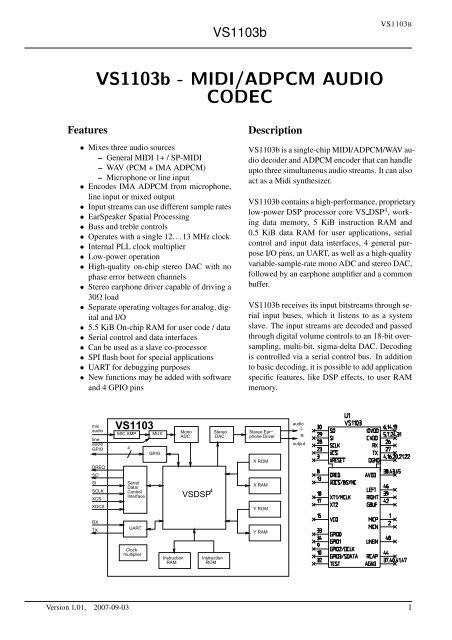
<strong>VS1103</strong>b<strong>VS1103</strong>B<strong>VS1103</strong>b - MIDI/ADPCM AUDIOCODECFeatures• Mixes three audio sources– General MIDI 1+ / SP-MIDI– WAV (PCM + IMA ADPCM)– Microphone or line input• Encodes IMA ADPCM from microphone,line input or mixed output• Input streams can use different sample rates• EarSpeaker Spatial Processing• Bass and treble controls• Operates with a single 12. . . 13 MHz clock• Internal PLL clock multiplier• Low-power operation• High-quality on-chip stereo DAC with nophase error between channels• Stereo earphone driver capable of driving a30Ω load• Separate operating voltages for analog, digitaland I/O• 5.5 KiB On-chip RAM for user code / data• Serial control and data interfaces• Can be used as a slave co-processor• SPI flash boot for special applications• UART for debugging purposes• New functions may be added with softwareand 4 GPIO pinsDescription<strong>VS1103</strong>b is a single-chip MIDI/ADPCM/WAV audiodecoder and ADPCM encoder that can handleupto three simultaneous audio streams. It can alsoact as a Midi synthesizer.<strong>VS1103</strong>b contains a high-performance, proprietarylow-power DSP processor core VS DSP 4 , workingdata memory, 5 KiB instruction RAM and0.5 KiB data RAM for user applications, serialcontrol and input data interfaces, 4 general purposeI/O pins, an UART, as well as a high-qualityvariable-sample-rate mono ADC and stereo DAC,followed by an earphone amplifier and a commonbuffer.<strong>VS1103</strong>b receives its input bitstreams through serialinput buses, which it listens to as a systemslave. The input streams are decoded and passedthrough digital volume controls to an 18-bit oversampling,multi-bit, sigma-delta DAC. Decodingis controlled via a serial control bus. In additionto basic decoding, it is possible to add applicationspecific features, like DSP effects, to user RAMmemory.micaudiolineaudioGPIO<strong>VS1103</strong>MIC AMP4MUXGPIOMonoADCStereoDACStereo Ear−phone DriveraudioLRoutputDREQX ROMSOSISCLKXCSSerialData/ControlInterfaceVSDSP 4X RAMXDCSY ROMRXTXUARTY RAMClockmultiplierInstructionRAMInstructionROMVersion 1.01, 2007-09-03 1
<strong>VLSI</strong><strong>Solution</strong> y<strong>VS1103</strong>b<strong>VS1103</strong>BCONTENTSContents1 Disclaimer 82 Definitions 83 Characteristics & Specifications 93.1 Absolute Maximum Ratings . . . . . . . . . . . . . . . . . . . . . . . . . . . . . . . . 93.2 Recommended Operating Conditions . . . . . . . . . . . . . . . . . . . . . . . . . . . . 93.3 Analog Characteristics . . . . . . . . . . . . . . . . . . . . . . . . . . . . . . . . . . . 103.4 Power Consumption . . . . . . . . . . . . . . . . . . . . . . . . . . . . . . . . . . . . . 113.5 Digital Characteristics . . . . . . . . . . . . . . . . . . . . . . . . . . . . . . . . . . . 113.6 Switching Characteristics - Boot Initialization . . . . . . . . . . . . . . . . . . . . . . . 114 Packages and Pin Descriptions 124.1 Packages . . . . . . . . . . . . . . . . . . . . . . . . . . . . . . . . . . . . . . . . . . 124.1.1 LQFP-48 . . . . . . . . . . . . . . . . . . . . . . . . . . . . . . . . . . . . . . 124.1.2 BGA-49 . . . . . . . . . . . . . . . . . . . . . . . . . . . . . . . . . . . . . . . 124.2 LQFP-48 and BGA-49 Pin Descriptions . . . . . . . . . . . . . . . . . . . . . . . . . . 135 SPI Buses 155.1 General . . . . . . . . . . . . . . . . . . . . . . . . . . . . . . . . . . . . . . . . . . . 155.2 SPI Bus Pin Descriptions . . . . . . . . . . . . . . . . . . . . . . . . . . . . . . . . . . 155.2.1 VS1002 Native Modes (New Mode) . . . . . . . . . . . . . . . . . . . . . . . . 155.2.2 VS1001 Compatibility Mode . . . . . . . . . . . . . . . . . . . . . . . . . . . . 155.3 Data Request Pin DREQ . . . . . . . . . . . . . . . . . . . . . . . . . . . . . . . . . . 165.4 Serial Protocol for Serial Data Interface (SDI) . . . . . . . . . . . . . . . . . . . . . . . 16Version 1.01, 2007-09-03 2
<strong>VLSI</strong><strong>Solution</strong> y<strong>VS1103</strong>b<strong>VS1103</strong>BCONTENTS6.6 SCI Registers . . . . . . . . . . . . . . . . . . . . . . . . . . . . . . . . . . . . . . . . 286.6.1 SCI MODE (RW) . . . . . . . . . . . . . . . . . . . . . . . . . . . . . . . . . 296.6.2 SCI STATUS (RW) . . . . . . . . . . . . . . . . . . . . . . . . . . . . . . . . . 316.6.3 SCI BASS (RW) . . . . . . . . . . . . . . . . . . . . . . . . . . . . . . . . . . 316.6.4 SCI CLOCKF (RW) . . . . . . . . . . . . . . . . . . . . . . . . . . . . . . . . 326.6.5 SCI DECODE TIME (RW) . . . . . . . . . . . . . . . . . . . . . . . . . . . . 336.6.6 SCI AUDATA (RW) . . . . . . . . . . . . . . . . . . . . . . . . . . . . . . . . 336.6.7 SCI WRAM (RW) . . . . . . . . . . . . . . . . . . . . . . . . . . . . . . . . . 336.6.8 SCI WRAMADDR (W) . . . . . . . . . . . . . . . . . . . . . . . . . . . . . . 336.6.9 SCI IN0 and SCI IN1 (R) . . . . . . . . . . . . . . . . . . . . . . . . . . . . . 346.6.10 SCI AIADDR (RW) . . . . . . . . . . . . . . . . . . . . . . . . . . . . . . . . 346.6.11 SCI VOL (RW) . . . . . . . . . . . . . . . . . . . . . . . . . . . . . . . . . . . 346.6.12 SCI MIXERVOL (RW) . . . . . . . . . . . . . . . . . . . . . . . . . . . . . . 356.6.13 SCI ADPCMRECCTL (RW) . . . . . . . . . . . . . . . . . . . . . . . . . . . 356.6.14 SCI AICTRL[x] (RW) . . . . . . . . . . . . . . . . . . . . . . . . . . . . . . . 367 Operation 377.1 Clocking . . . . . . . . . . . . . . . . . . . . . . . . . . . . . . . . . . . . . . . . . . . 377.2 Hardware Reset . . . . . . . . . . . . . . . . . . . . . . . . . . . . . . . . . . . . . . . 377.3 Software Reset . . . . . . . . . . . . . . . . . . . . . . . . . . . . . . . . . . . . . . . 377.4 ADPCM Recording . . . . . . . . . . . . . . . . . . . . . . . . . . . . . . . . . . . . . 387.4.1 Activating ADPCM Recording . . . . . . . . . . . . . . . . . . . . . . . . . . . 387.4.2 Reading IMA ADPCM Data . . . . . . . . . . . . . . . . . . . . . . . . . . . . 387.4.3 Adding a RIFF Header . . . . . . . . . . . . . . . . . . . . . . . . . . . . . . . 397.4.4 Playing ADPCM Data . . . . . . . . . . . . . . . . . . . . . . . . . . . . . . . 40Version 1.01, 2007-09-03 4
<strong>VLSI</strong><strong>Solution</strong> y<strong>VS1103</strong>b<strong>VS1103</strong>BCONTENTS7.4.5 Sample Rate Considerations . . . . . . . . . . . . . . . . . . . . . . . . . . . . 407.4.6 Example Code . . . . . . . . . . . . . . . . . . . . . . . . . . . . . . . . . . . 407.5 SPI Boot . . . . . . . . . . . . . . . . . . . . . . . . . . . . . . . . . . . . . . . . . . . 427.6 Play/Decode . . . . . . . . . . . . . . . . . . . . . . . . . . . . . . . . . . . . . . . . . 427.7 Feeding PCM data . . . . . . . . . . . . . . . . . . . . . . . . . . . . . . . . . . . . . 427.8 SDI Tests . . . . . . . . . . . . . . . . . . . . . . . . . . . . . . . . . . . . . . . . . . 427.8.1 Sine Test . . . . . . . . . . . . . . . . . . . . . . . . . . . . . . . . . . . . . . 437.8.2 Pin Test . . . . . . . . . . . . . . . . . . . . . . . . . . . . . . . . . . . . . . . 437.8.3 Memory Test . . . . . . . . . . . . . . . . . . . . . . . . . . . . . . . . . . . . 447.8.4 SCI Test . . . . . . . . . . . . . . . . . . . . . . . . . . . . . . . . . . . . . . . 448 <strong>VS1103</strong>b Registers 458.1 Who Needs to Read This Chapter . . . . . . . . . . . . . . . . . . . . . . . . . . . . . 458.2 The Processor Core . . . . . . . . . . . . . . . . . . . . . . . . . . . . . . . . . . . . . 458.3 <strong>VS1103</strong>b Memory Map . . . . . . . . . . . . . . . . . . . . . . . . . . . . . . . . . . . 458.4 SCI Registers . . . . . . . . . . . . . . . . . . . . . . . . . . . . . . . . . . . . . . . . 458.5 Serial Data Registers . . . . . . . . . . . . . . . . . . . . . . . . . . . . . . . . . . . . 458.6 DAC Registers . . . . . . . . . . . . . . . . . . . . . . . . . . . . . . . . . . . . . . . 468.7 GPIO Registers . . . . . . . . . . . . . . . . . . . . . . . . . . . . . . . . . . . . . . . 478.8 Interrupt Registers . . . . . . . . . . . . . . . . . . . . . . . . . . . . . . . . . . . . . 488.9 A/D Modulator Registers . . . . . . . . . . . . . . . . . . . . . . . . . . . . . . . . . . 498.10 Watchdog v1.0 2002-08-26 . . . . . . . . . . . . . . . . . . . . . . . . . . . . . . . . . . 508.10.1 Registers . . . . . . . . . . . . . . . . . . . . . . . . . . . . . . . . . . . . . . 508.11 UART v1.0 2002-04-23 . . . . . . . . . . . . . . . . . . . . . . . . . . . . . . . . . . . 518.11.1 Registers . . . . . . . . . . . . . . . . . . . . . . . . . . . . . . . . . . . . . . 51Version 1.01, 2007-09-03 5
<strong>VLSI</strong><strong>Solution</strong> y<strong>VS1103</strong>b<strong>VS1103</strong>BCONTENTS8.11.2 Status UARTx STATUS . . . . . . . . . . . . . . . . . . . . . . . . . . . . . . 518.11.3 Data UARTx DATA . . . . . . . . . . . . . . . . . . . . . . . . . . . . . . . . 528.11.4 Data High UARTx DATAH . . . . . . . . . . . . . . . . . . . . . . . . . . . . 528.11.5 Divider UARTx DIV . . . . . . . . . . . . . . . . . . . . . . . . . . . . . . . . 528.11.6 Interrupts and Operation . . . . . . . . . . . . . . . . . . . . . . . . . . . . . . 538.12 Timers v1.0 2002-04-23 . . . . . . . . . . . . . . . . . . . . . . . . . . . . . . . . . . . 548.12.1 Registers . . . . . . . . . . . . . . . . . . . . . . . . . . . . . . . . . . . . . . 548.12.2 Configuration TIMER CONFIG . . . . . . . . . . . . . . . . . . . . . . . . . . 548.12.3 Configuration TIMER ENABLE . . . . . . . . . . . . . . . . . . . . . . . . . . 558.12.4 Timer X Startvalue TIMER Tx[L/H] . . . . . . . . . . . . . . . . . . . . . . . 558.12.5 Timer X Counter TIMER TxCNT[L/H] . . . . . . . . . . . . . . . . . . . . . . 558.12.6 Interrupts . . . . . . . . . . . . . . . . . . . . . . . . . . . . . . . . . . . . . . 558.13 System Vector Tags . . . . . . . . . . . . . . . . . . . . . . . . . . . . . . . . . . . . . 568.13.1 AudioInt, 0x20 . . . . . . . . . . . . . . . . . . . . . . . . . . . . . . . . . . . 568.13.2 SciInt, 0x21 . . . . . . . . . . . . . . . . . . . . . . . . . . . . . . . . . . . . . 568.13.3 DataInt, 0x22 . . . . . . . . . . . . . . . . . . . . . . . . . . . . . . . . . . . . 568.13.4 ModuInt, 0x23 . . . . . . . . . . . . . . . . . . . . . . . . . . . . . . . . . . . 568.13.5 TxInt, 0x24 . . . . . . . . . . . . . . . . . . . . . . . . . . . . . . . . . . . . . 578.13.6 RxInt, 0x25 . . . . . . . . . . . . . . . . . . . . . . . . . . . . . . . . . . . . . 578.13.7 Timer0Int, 0x26 . . . . . . . . . . . . . . . . . . . . . . . . . . . . . . . . . . 578.13.8 Timer1Int, 0x27 . . . . . . . . . . . . . . . . . . . . . . . . . . . . . . . . . . 578.13.9 UserCodec, 0x0 . . . . . . . . . . . . . . . . . . . . . . . . . . . . . . . . . . . 588.14 System Vector Functions . . . . . . . . . . . . . . . . . . . . . . . . . . . . . . . . . . 588.14.1 WriteIRam(), 0x2 . . . . . . . . . . . . . . . . . . . . . . . . . . . . . . . . . . 58Version 1.01, 2007-09-03 6
<strong>VLSI</strong><strong>Solution</strong> y<strong>VS1103</strong>b<strong>VS1103</strong>BLIST OF FIGURES8.14.2 ReadIRam(), 0x4 . . . . . . . . . . . . . . . . . . . . . . . . . . . . . . . . . . 588.14.3 DataBytes(), 0x6 . . . . . . . . . . . . . . . . . . . . . . . . . . . . . . . . . . 588.14.4 GetDataByte(), 0x8 . . . . . . . . . . . . . . . . . . . . . . . . . . . . . . . . . 598.14.5 GetDataWords(), 0xa . . . . . . . . . . . . . . . . . . . . . . . . . . . . . . . . 598.14.6 Reboot(), 0xc . . . . . . . . . . . . . . . . . . . . . . . . . . . . . . . . . . . . 599 Document Version Changes 6010 Contact Information 61List of Figures1 Pin Configuration, LQFP-48. . . . . . . . . . . . . . . . . . . . . . . . . . . . . . . . . 122 Pin Configuration, BGA-49. . . . . . . . . . . . . . . . . . . . . . . . . . . . . . . . . 123 BSYNC Signal - one byte transfer. . . . . . . . . . . . . . . . . . . . . . . . . . . . . . 174 BSYNC Signal - two byte transfer. . . . . . . . . . . . . . . . . . . . . . . . . . . . . . 175 SCI Word Read . . . . . . . . . . . . . . . . . . . . . . . . . . . . . . . . . . . . . . . 186 SCI Word Write . . . . . . . . . . . . . . . . . . . . . . . . . . . . . . . . . . . . . . . 187 SCI Multiple Word Write . . . . . . . . . . . . . . . . . . . . . . . . . . . . . . . . . . 198 SPI Timing Diagram. . . . . . . . . . . . . . . . . . . . . . . . . . . . . . . . . . . . . 209 Two SCI Operations. . . . . . . . . . . . . . . . . . . . . . . . . . . . . . . . . . . . . 2110 Two SDI Bytes. . . . . . . . . . . . . . . . . . . . . . . . . . . . . . . . . . . . . . . . 2111 Two SDI Bytes Separated By an SCI Operation. . . . . . . . . . . . . . . . . . . . . . . 2212 Normal Data Flow of <strong>VS1103</strong>b, Part 1. . . . . . . . . . . . . . . . . . . . . . . . . . . . 2613 Normal Data Flow of <strong>VS1103</strong>b, Part 2. . . . . . . . . . . . . . . . . . . . . . . . . . . . 2714 User’s Memory Map. . . . . . . . . . . . . . . . . . . . . . . . . . . . . . . . . . . . . 4615 RS232 Serial Interface Protocol . . . . . . . . . . . . . . . . . . . . . . . . . . . . . . 51Version 1.01, 2007-09-03 7
<strong>VLSI</strong><strong>Solution</strong> y<strong>VS1103</strong>b<strong>VS1103</strong>B1. DISCLAIMER1 DisclaimerAll properties and figures are subject to change.2 DefinitionsB Byte, 8 bits.b Bit.Ki “Kibi” = 2 10 = 1024 (IEC 60027-2).Mi “Mebi” = 2 20 = 1048576 (IEC 60027-2).VS DSP <strong>VLSI</strong> <strong>Solution</strong>’s DSP core.W Word. In VS DSP, instruction words are 32-bit and data words are 16-bit wide.Version 1.01, 2007-09-03 8
<strong>VLSI</strong><strong>Solution</strong> y<strong>VS1103</strong>b<strong>VS1103</strong>B3. CHARACTERISTICS & SPECIFICATIONS3 Characteristics & Specifications3.1 Absolute Maximum RatingsParameter Symbol Min Max UnitAnalog Positive Supply AVDD -0.3 2.85 VDigital Positive Supply CVDD -0.3 2.7 VI/O Positive Supply IOVDD -0.3 3.6 VCurrent at Any Digital Output ±50 mAVoltage at Any Digital Input -0.3 IOVDD+0.3 1 VOperating Temperature -40 +85 ◦ CStorage Temperature -65 +150 ◦ C1 Must not exceed 3.6 V3.2 Recommended Operating ConditionsParameter Symbol Min Typ Max UnitAmbient Operating Temperature -40 +85 ◦ CAnalog and Digital Ground 1 AGND DGND 0.0 VPositive Analog AVDD 2.6 2.8 2.85 VPositive Digital CVDD 2.4 2.5 2.7 VI/O Voltage IOVDD CVDD-0.6V 2.8 3.6 VInput Clock Frequency 2 XTALI 12 12.288 13 MHzInternal Clock Frequency CLKI 12 36.864 52.0 4 MHzInternal Clock Multiplier 3 1.0× 3.0× 4.5× 4Master Clock Duty Cycle 40 50 60 %1 Must be connected together as close the device as possible for latch-up immunity.2 The maximum sample rate that can be played with correct speed is XTALI/256.Thus, XTALI must be at least 12.288 MHz to be able to play 48 kHz at correct speed.For other implications rising from not using a 12.288 MHz clock, see Chapter 7.4.5.3 Reset value is 1.0×. Recommended SC MULT=4.0×.Performance may be poor if SC MULT< 3.5.4 52.0 MHz is the maximum clock for the full CVDD range.(4.0 × 12.288 MHz=49.152 MHz or 3.5 × 13.0 MHz=45.5 MHz)Version 1.01, 2007-09-03 9
<strong>VLSI</strong><strong>Solution</strong> y<strong>VS1103</strong>b<strong>VS1103</strong>B3. CHARACTERISTICS & SPECIFICATIONS3.3 Analog CharacteristicsUnless otherwise noted: AVDD=2.5..2.85V, CVDD=2.4..2.7V, IOVDD=CVDD-0.6V..3.6V, TA=-25..+70 ◦ C,XTALI=12..13MHz, Internal Clock Multiplier 3.5×. DAC tested with 1307.894 Hz full-scale outputsinewave, measurement bandwidth 20..20000 Hz, analog output load: LEFT to GBUF 30Ω, RIGHT toGBUF 30Ω. Microphone test amplitude 50 mVpp, f s =1 kHz, Line input test amplitude 1.1 V, f s =1 kHz.Parameter Symbol Min Typ Max UnitDAC Resolution 18 bitsTotal Harmonic Distortion THD 0.1 0.3 %Dynamic Range (DAC unmuted, A-weighted) IDR 90 dBS/N Ratio (full scale signal) SNR 70 dBInterchannel Isolation (Cross Talk) 50 75 dBInterchannel Isolation (Cross Talk), with GBUF 40 dBInterchannel Gain Mismatch -0.5 0.5 dBFrequency Response -0.1 0.1 dBFull Scale Output Voltage (Peak-to-peak) 1.3 1.5 1 1.7 VppDeviation from Linear Phase 5◦Analog Output Load Resistance AOLR 16 30 2 ΩAnalog Output Load Capacitance 100 pFMicrophone input amplifier gain MICG 26 dBMicrophone input amplitude 50 140 3 mVpp ACMicrophone Total Harmonic Distortion MTHD 0.02 0.10 %Microphone S/N Ratio MSNR 50 62 dBLine input amplitude 2200 2800 3 mVpp ACLine input Total Harmonic Distortion LTHD 0.06 0.10 %Line input S/N Ratio LSNR 60 68 dBLine and Microphone input impedances 100 kΩ1 3.0 volts can be achieved with +-to-+ wiring for mono difference sound.2 AOLR may be much lower, but below Typical distortion performance may be compromised.3 Harmonic Distortion increases above typical amplitude.Version 1.01, 2007-09-03 10
<strong>VLSI</strong><strong>Solution</strong> y<strong>VS1103</strong>b<strong>VS1103</strong>B3. CHARACTERISTICS & SPECIFICATIONS3.4 Power ConsumptionTBD3.5 Digital CharacteristicsParameter Symbol Min Typ Max UnitHigh-Level Input Voltage 0.7×IOVDD IOVDD+0.3 1 VLow-Level Input Voltage -0.2 0.3×IOVDD VHigh-Level Output Voltage at I O = -1.0 mA 0.7×IOVDD VLow-Level Output Voltage at I O = 1.0 mA 0.3×IOVDD VInput Leakage Current -1.0 1.0 µACLKI6MHzSPI Input Clock Frequency 2Rise time of all output pins, load = 50 pF 50 ns1 Must not exceed 3.6V2 Value for SCI reads. SCI and SDI writes allow CLKI4.3.6 Switching Characteristics - Boot InitializationParameter Symbol Min Max UnitXRESET active time 2 XTALIXRESET inactive to software ready 16600 50000 1 XTALIPower on reset, rise time to CVDD 10 V/s1 DREQ rises when initialization is complete. You should not send any data or commands before that.Version 1.01, 2007-09-03 11
1.10 REF<strong>VLSI</strong><strong>Solution</strong> y<strong>VS1103</strong>b<strong>VS1103</strong>B4. PACKAGES AND PIN DESCRIPTIONS4 Packages and Pin Descriptions4.1 PackagesBoth LPQFP-48 and BGA-49 are lead (Pb) free and also RoHS compliant packages. RoHS is a shortname of Directive 2002/95/EC on the restriction of the use of certain hazardous substances in electricaland electronic equipment.4.1.1 LQFP-48148Figure 1: Pin Configuration, LQFP-48.LQFP-48 package dimensions are at http://www.vlsi.fi/ .4.1.2 BGA-49A1 BALL PAD CORNER1 2 3 4 5 6 7ABCDE0.80 TYP4.807.00FG1.10 REF0.80 TYP4.807.00TOP VIEWFigure 2: Pin Configuration, BGA-49.BGA-49 package dimensions are at http://www.vlsi.fi/ .Version 1.01, 2007-09-03 12
<strong>VLSI</strong><strong>Solution</strong> y<strong>VS1103</strong>b<strong>VS1103</strong>B4. PACKAGES AND PIN DESCRIPTIONS4.2 LQFP-48 and BGA-49 Pin DescriptionsPin NameLQFP-48 PinBGA49BallPinTypeFunctionMICP 1 C3 AI Positive differential microphone input, self-biasingMICN 2 C2 AI Negative differential microphone input, self-biasingXRESET 3 B1 DI Active low asynchronous resetDGND0 4 D2 DGND Core & I/O groundCVDD0 5 C1 CPWR Core power supplyIOVDD0 6 D3 IOPWR I/O power supplyCVDD1 7 D1 CPWR Core power supplyDREQ 8 E2 DO Data request, input busGPIO2 / DCLK 1 9 E1 DIO General purpose IO 2 / serial input data bus clockGPIO3 / SDATA 1 10 F2 DIO General purpose IO 3 / serial data inputXDCS / BSYNC 1 13 E3 DI Data chip select / byte syncIOVDD1 14 F3 IOPWR I/O power supplyVCO 15 G2 DO For testing only (Clock VCO output)DGND1 16 F4 DGND Core & I/O groundXTALO 17 G3 AO Crystal outputXTALI 18 E4 AI Crystal inputIOVDD2 19 G4 IOPWR I/O power supplyIOVDD3 F5 IOPWR I/O power supplyDGND2 20 DGND Core & I/O groundDGND3 21 G5 DGND Core & I/O groundDGND4 22 F6 DGND Core & I/O groundXCS 23 G6 DI Chip select input (active low)CVDD2 24 G7 CPWR Core power supplyRX 26 E6 DI UART receive, connect to IOVDD if not usedTX 27 F7 DO UART transmitSCLK 28 D6 DI Clock for serial busSI 29 E7 DI Serial inputSO 30 D5 DO3 Serial outputCVDD3 31 D7 CPWR Core power supplyTEST 32 C6 DI Reserved for test, connect to IOVDDGPIO0 / SPIBOOT 33 C7 DIO General purpose IO 0 / SPIBOOT, use 100 kΩ pull-downresistor 2GPIO1 34 B6 DIO General purpose IO 1AGND0 37 C5 APWR Analog ground, low-noise referenceAVDD0 38 B5 APWR Analog power supplyRIGHT 39 A6 AO Right channel outputAGND1 40 B4 APWR Analog groundAGND2 41 A5 APWR Analog groundGBUF 42 C4 AO Common buffer for headphonesAVDD1 43 A4 APWR Analog power supplyRCAP 44 B3 AIO Filtering capacitance for referenceAVDD2 45 A3 APWR Analog power supplyLEFT 46 B2 AO Left channel outputAGND3 47 A2 APWR Analog groundLINEIN 48 A1 AI Line input1 First pin function is active in New Mode, latter in Compatibility Mode.2 Unless pull-down resistor is used, SPI Boot is tried. See Chapter 7.5 for details.Version 1.01, 2007-09-03 13
<strong>VLSI</strong><strong>Solution</strong> y<strong>VS1103</strong>b<strong>VS1103</strong>B4. PACKAGES AND PIN DESCRIPTIONSPin types:TypeDIDODIODO3AIDescriptionDigital input, CMOS Input PadDigital output, CMOS Input PadDigital input/outputDigital output, CMOS Tri-stated Output PadAnalog inputTypeAOAIOAPWRDGNDCPWRIOPWRDescriptionAnalog outputAnalog input/outputAnalog power supply pinCore or I/O ground pinCore power supply pinI/O power supply pinIn BGA-49, no-connect balls are A7, B7, D4, E5, F1, G1.In LQFP-48, no-connect pins are 11, 12, 25, 35, 36.Version 1.01, 2007-09-03 14
<strong>VLSI</strong><strong>Solution</strong> y<strong>VS1103</strong>b<strong>VS1103</strong>B5. SPI BUSES5 SPI Buses5.1 GeneralThe SPI Bus - that was originally used in some Motorola devices - has been used for both <strong>VS1103</strong>b’sSerial Data Interface SDI (Chapters 5.4 and 6.4) and Serial Control Interface SCI (Chapters 5.5 and 6.5).5.2 SPI Bus Pin Descriptions5.2.1 VS1002 Native Modes (New Mode)These modes are active on <strong>VS1103</strong>b when SM SDINEW is set to 1 (default at startup). DCLK, SDATAand BSYNC are replaced with GPIO2, GPIO3 and XDCS, respectively.SDI Pin SCI Pin DescriptionXDCS XCS Active low chip select input. A high level forces the serial interface intostandby mode, ending the current operation. A high level also forces serialoutput (SO) to high impedance state. If SM SDISHARE is 1, pinXDCS is not used, but the signal is generated internally by invertingXCS.SCK Serial clock input. The serial clock is also used internally as the masterclock for the register interface.SCK can be gated or continuous. In either case, the first rising clock edgeafter XCS has gone low marks the first bit to be written.SI Serial input. If a chip select is active, SI is sampled on the rising CLK edge.- SO Serial output. In reads, data is shifted out on the falling SCK edge.In writes SO is at a high impedance state.5.2.2 VS1001 Compatibility ModeThis mode is active when SM SDINEW is set to 0. In this mode, DCLK, SDATA and BSYNC are active.SDI Pin SCI Pin Description- XCS Active low chip select input. A high level forces the serial interface intostandby mode, ending the current operation. A high level also forces serialoutput (SO) to high impedance state.BSYNC - SDI data is synchronized with a rising edge of BSYNC.DCLK SCK Serial clock input. The serial clock is also used internally as the masterclock for the register interface.SCK can be gated or continuous. In either case, the first rising clock edgeafter XCS has gone low marks the first bit to be written.SDATA SI Serial input. SI is sampled on the rising SCK edge, if XCS is low.- SO Serial output. In reads, data is shifted out on the falling SCK edge.In writes SO is at a high impedance state.Version 1.01, 2007-09-03 15
<strong>VLSI</strong><strong>Solution</strong> y<strong>VS1103</strong>b<strong>VS1103</strong>B5. SPI BUSES5.3 Data Request Pin DREQThe DREQ pin/signal is used to signal if <strong>VS1103</strong>b’s SDI FIFO is capable of receiving data. If DREQ ishigh, <strong>VS1103</strong>b can take at least 32 bytes of SDI data or one SCI command.Because of a 32-byte safety area, the sender may send upto 32 bytes of SDI data at a time withoutchecking the status of DREQ, making controlling <strong>VS1103</strong>b easier for low-speed microcontrollers. IfSARC DREQ512 is set, the safety area is 512 bytes (see Chapter 6.6.13).Note: DREQ may turn low or high at any time, even during a byte transmission. Thus, DREQ shouldonly be used to decide whether to send more bytes. It should not abort a transmission that has alreadystarted.Note: In VS10XX products upto VS1002, DREQ was only used for SDI. In <strong>VS1103</strong>b DREQ is alsoused to tell the status of SCI.5.4 Serial Protocol for Serial Data Interface (SDI)5.4.1 GeneralThe serial data interface operates in slave mode so the DCLK signal must be generated by an externalcircuit.Data (SDATA signal) can be clocked in at either the rising or falling edge of DCLK (Chapter 6.6).<strong>VS1103</strong>b assumes its data input to be byte-sychronized. SDI bytes may be transmitted either MSb orLSb first, depending of SCI MODE (Chapter 6.6.1).5.4.2 SDI in VS1002 Native Modes (Recommended)In VS1002 native modes (SM NEWMODE is 1), byte synchronization is achieved by XDCS. The state ofXDCS may not change while a data byte transfer is in progress. To always maintain data synchronizationeven if there may be glitches in the boards using <strong>VS1103</strong>b, it is recommended to turn XDCS every nowand then, for instance once after every flash data block or a few kilobytes, just to keep sure the host and<strong>VS1103</strong>b are in sync.If SM SDISHARE is 1, the XDCS signal is internally generated by inverting the XCS input.For new designs, using VS1002 native modes are recommended.Version 1.01, 2007-09-03 16
<strong>VLSI</strong><strong>Solution</strong> y<strong>VS1103</strong>b<strong>VS1103</strong>B5. SPI BUSES5.4.3 SDI in VS1001 Compatibility ModeBSYNCSDATAD7 D6 D5 D4 D3 D2 D1 D0DCLKFigure 3: BSYNC Signal - one byte transfer.When <strong>VS1103</strong>b is running in VS1001 compatibility mode, a BSYNC signal must be generated to ensurecorrect bit-alignment of the input bitstream. The first DCLK sampling edge (rising or falling, dependingon selected polarity), during which the BSYNC is high, marks the first bit of a byte (LSB, if LSB-firstorder is used, MSB, if MSB-first order is used). If BSYNC is ’1’ when the last bit is received, the receiverstays active and next 8 bits are also received.BSYNCSDATAD7 D6 D5 D4 D3 D2 D1 D0 D7 D6 D5 D4 D3 D2 D1 D0DCLKFigure 4: BSYNC Signal - two byte transfer.5.4.4 Passive SDI ModeIf SM NEWMODE is 0 and SM SDISHARE is 1, the operation is otherwise like the VS1001 compatibilitymode, but bits are only received while the BSYNC signal is ’1’. Rising edge of BSYNC is stillused for synchronization.5.5 Serial Protocol for Serial Command Interface (SCI)5.5.1 GeneralThe serial bus protocol for the Serial Command Interface SCI (Chapter 6.5) consists of an instructionbyte, address byte and one 16-bit data word. Each read or write operation can read or write a singleregister. Data bits are read at the rising edge, so the user should update data at the falling edge. Bytes arealways sent MSb first. XCS should be low for the full duration of the operation, but you can have pausesbetween bits if needed.The operation is specified by an 8-bit instruction opcode. The supported instructions are read and write.See table below.InstructionName Opcode OperationREAD 0b0000 0011 Read dataWRITE 0b0000 0010 Write dataNote: <strong>VS1103</strong>b sets DREQ low after each SCI operation. The duration depends on the operation. It isnot allowed to finish a new SCI/SDI operation before DREQ is high again.Version 1.01, 2007-09-03 17
<strong>VLSI</strong><strong>Solution</strong> y<strong>VS1103</strong>b<strong>VS1103</strong>B5. SPI BUSES5.5.2 SCI ReadXCSSCK0 1 2 3 4 5 6 7 8 9 10 11 12 13 14 15 16 1730 31SI0 0 0 0 0 0 1 1 0 0 0 03 2 1 0don’t caredon’t careinstruction (read)addressdata outSO0 0 0 0 0 0 0 0 0 0 0 0 0 0 0 015 14 1 0XexecutionDREQFigure 5: SCI Word Read<strong>VS1103</strong>b registers are read from using the following sequence, as shown in Figure 5. First, XCS line ispulled low to select the device. Then the READ opcode (0x3) is transmitted via the SI line followed byan 8-bit word address. After the address has been read in, any further data on SI is ignored by the chip.The 16-bit data corresponding to the received address will be shifted out onto the SO line.XCS should be driven high after data has been shifted out.DREQ is driven low for a short while when in a read operation by the chip. This is a very short time anddoesn’t require special user attention.5.5.3 SCI WriteXCSSCK0 1 2 3 4 5 6 7 8 9 10 11 12 13 14 15 16 1730 31SI0 0 0 0 0 0 1 0 0 0 0 03 2 1 0 15 141 0Xinstruction (write)addressdata outSO 0 0 0 0 0 0 0 0 0 0 0 0 0 0 0 0 0 0 0 0 XexecutionDREQFigure 6: SCI Word Write<strong>VS1103</strong>b registers are written from using the following sequence, as shown in Figure 6. First, XCS lineis pulled low to select the device. Then the WRITE opcode (0x2) is transmitted via the SI line followedby an 8-bit word address.Version 1.01, 2007-09-03 18
<strong>VLSI</strong><strong>Solution</strong> y<strong>VS1103</strong>b<strong>VS1103</strong>B5. SPI BUSESAfter the word has been shifted in and the last clock has been sent, XCS should be pulled high to end theWRITE sequence.After the last bit has been sent, DREQ is driven low for the duration of the register update, marked“execution” in the figure. The time varies depending on the register and its contents (see table in Chapter6.6 for details). If the maximum time is longer than what it takes from the microcontroller to feedthe next SCI command or SDI byte, status of DREQ must be checked before finishing the next SCI/SDIoperation.5.5.4 SCI Multiple WriteXCSSCK0 1 2 3 4 5 6 7 8 9 10 11 12 13 14 15 16 1729 30 3132 33m−2m−1SI0 0 0 0 0 0 1 0 0 0 0 03 2 1 015 141 0 15 14X1 0Xinstruction (write)addressSO 0 0 0 0 0 0 0 0 0 0 0 0 0 0 0 0 0 0data out 1 data out 2 d.out n0 0 0 00 0 XexecutionexecutionDREQFigure 7: SCI Multiple Word Write<strong>VS1103</strong>b allows for the user to send multiple words to the same SCI register, which allows fast SCIuploads, shown in Figure 7. The main difference with a single write is that instead of bringing XCS upafter sending the last bit of a data word, the next data word is sent immediately. After the last data word,XCS is driven high as with a single word write.After the last bit of a word has been sent, DREQ is driven low for the duration of the register update,marked “execution” in the figure. The time varies depending on the register and its contents (see tablein Chapter 6.6 for details). If the maximum time is longer than what it takes from the microcontrollerto feed the next SCI command or SDI byte, status of DREQ must be checked before finishing the nextSCI/SDI operation.Version 1.01, 2007-09-03 19
<strong>VLSI</strong><strong>Solution</strong> y<strong>VS1103</strong>b<strong>VS1103</strong>B5. SPI BUSES5.6 SPI Timing DiagramtXCSStWLtWHtXCSHXCS0 1 14 15 1630 31tXCSSCKSISOtZtHtSUtVtDISFigure 8: SPI Timing Diagram.Symbol Min Max UnittXCSS 5 nstSU -26 nstH 2 CLKI cyclestZ 0 nstWL 2 CLKI cyclestWH 2 CLKI cyclestV 2 (+ 25ns 1 ) CLKI cyclestXCSH -26 nstXCS 2 CLKI cyclestDIS 10 ns1 25ns is when pin loaded with 100pF capacitance. The time is shorter with lower capacitance.Note: As tWL and tWH, as well as tH require at least 2 clock cycles, the maximum speed for the SPIbus that can easily be used is 1/6 of <strong>VS1103</strong>b’s internal clock speed CLKI. Slightly higher speed can beachieved with very careful timing tuning. For details, see Application Notes for VS10XX.Note: Although the timing is derived from the internal clock CLKI, the system always starts up in 1.0×mode, thus CLKI=XTALI.Note: Negative numbers mean that the signal can change in different order from what is shown in thediagram.Version 1.01, 2007-09-03 20
<strong>VLSI</strong><strong>Solution</strong> y<strong>VS1103</strong>b<strong>VS1103</strong>B5. SPI BUSES5.7 SPI Examples with SM SDINEW and SM SDISHARED set5.7.1 Two SCI WritesSCI Write 1 SCI Write 2XCS0 1 2 3 30 3132 33 61 62 63SCKSI1 0 2 1 00 0 0 0 X0 0XDREQ up before finishing next SCI writeDREQFigure 9: Two SCI Operations.Figure 9 shows two consecutive SCI operations. Note that xCS must be raised to inactive state betweenthe writes. Also DREQ must be respected as shown in the figure.5.7.2 Two SDI BytesSDI Byte 1SDI Byte 2XCS0 1 2 36 7 8 9 13 14 15SCK7 6 5 4 3 1 0 7 6 5 2 1 0SIXDREQFigure 10: Two SDI Bytes.SDI data is synchronized with a raising edge of xCS as shown in Figure 10. However, every byte doesn’tneed separate synchronization.Version 1.01, 2007-09-03 21
<strong>VLSI</strong><strong>Solution</strong> y<strong>VS1103</strong>b<strong>VS1103</strong>B5. SPI BUSES5.7.3 SCI Operation in Middle of Two SDI BytesSDI ByteSCI OperationSDI ByteXCS0 178 9 39 40 41 46 47SCKSI7 6 5 10 00 7 6 5 1 0XDREQ high before end of next transferDREQFigure 11: Two SDI Bytes Separated By an SCI Operation.Figure 11 shows how an SCI operation is embedded in between SDI operations. xCS edges are used tosynchronize both SDI and SCI. Remember to respect DREQ as shown in the figure.Version 1.01, 2007-09-03 22
<strong>VLSI</strong><strong>Solution</strong> y<strong>VS1103</strong>b<strong>VS1103</strong>B6. FUNCTIONAL DESCRIPTION6 Functional Description6.1 Main Features<strong>VS1103</strong>b is based on a proprietary digital signal processor, VS DSP. It contains all the code and datamemory needed for WAV PCM + ADPCM audio decoding, MIDI synthesizer, together with serial interfaces,a multirate stereo audio DAC and analog output amplifiers and filters. Also ADPCM audioencoding is supported using a microphone amplifier and A/D converter. A UART is provided for debuggingpurposes.6.2 Supported Audio Codecs6.2.1 Supported RIFF WAV FormatsThe most common RIFF WAV subformats are supported.Format Name Supported Comments0x01 PCM + 16 and 8 bits, any sample rate ≤ 48kHz0x02 ADPCM -0x03 IEEE FLOAT -0x06 ALAW -0x07 MULAW -0x10 OKI ADPCM -0x11 IMA ADPCM + Any sample rate ≤ 48kHz0x15 DIGISTD -0x16 DIGIFIX -0x30 DOLBY AC2 -0x31 GSM610 -0x3b ROCKWELL ADPCM -0x3c ROCKWELL DIGITALK -0x40 G721 ADPCM -0x41 G728 CELP -0x50 MPEG -0x55 MPEGLAYER3 -0x64 G726 ADPCM -0x65 G722 ADPCM -Version 1.01, 2007-09-03 23
<strong>VLSI</strong><strong>Solution</strong> y<strong>VS1103</strong>b<strong>VS1103</strong>B6. FUNCTIONAL DESCRIPTION6.2.2 Supported MIDI FormatsGeneral MIDI and SP-MIDI format 0 files are played. Format 1 and 2 files must be converted to format0 by the user. The maximum simultaneous polyphony is 40 (peak polyphony 64). Actual polyphonydepends on the internal clock rate (which is user-selectable), the instruments used, and the possiblepostprocessing effects enabled, such as bass and treble enhancers. The polyphony restriction algorithmmakes use of the SP-MIDI MIP table, if present. MIDI implements click-avoiding smooth note removal.When run in Real Time RT-Midi mode without other signal paths, 36.86 MHz (3.0× input clock)achieves 16-26 simultaneous sustained notes. The instantaneous amount of notes can be larger. 36 MHzis a fair compromise between power consumption and quality, but higher clocks can be used to increasepolyphony. They are also needed if multiple signal paths are used.Reverb effect can be controlled by the user. In addition to reverb automatic and reverb off modes, 14different decay times can be selected. These roughly correspond to different room sizes. Also, eachmidi song decides how much effect each instrument gets. Because the reverb effect uses about 4 MHz ofprocessing power the automatic control enables reverb only when the internal clock is at least 3.0×.When EarSpeaker spatial processing is active, MIDI reverb is not used.<strong>VS1103</strong>b supports unique instruments in the whole GM1 instrument set and one bank of GM2 percussions.Version 1.01, 2007-09-03 24
<strong>VLSI</strong><strong>Solution</strong> y<strong>VS1103</strong>b<strong>VS1103</strong>B6. FUNCTIONAL DESCRIPTION<strong>VS1103</strong>b Melodic Intruments (GM1)1 Acoustic Grand Piano2 Bright Acoustic Piano3 Electric Grand Piano4 Honky-tonk Piano5 Electric Piano 16 Electric Piano 27 Harpsichord8 Clavi9 Celesta10 Glockenspiel11 Music Box12 Vibraphone13 Marimba14 Xylophone15 Tubular Bells16 Dulcimer17 Drawbar Organ18 Percussive Organ19 Rock Organ20 Church Organ21 Reed Organ22 Accordion23 Harmonica24 Tango Accordion25 Acoustic Guitar (nylon)26 Acoustic Guitar (steel)27 Electric Guitar (jazz)28 Electric Guitar (clean)29 Electric Guitar (muted)30 Overdriven Guitar31 Distortion Guitar32 Guitar Harmonics33 Acoustic Bass34 Electric Bass (finger)35 Electric Bass (pick)36 Fretless Bass37 Slap Bass 138 Slap Bass 239 Synth Bass 140 Synth Bass 241 Violin42 Viola43 Cello44 Contrabass45 Tremolo Strings46 Pizzicato Strings47 Orchestral Harp48 Timpani49 String Ensembles 150 String Ensembles 251 Synth Strings 152 Synth Strings 253 Choir Aahs54 Voice Oohs55 Synth Voice56 Orchestra Hit57 Trumpet58 Trombone59 Tuba60 Muted Trumpet61 French Horn62 Brass Section63 Synth Brass 164 Synth Brass 265 Soprano Sax66 Alto Sax67 Tenor Sax68 Baritone Sax69 Oboe70 English Horn71 Bassoon72 Clarinet73 Piccolo74 Flute75 Recorder76 Pan Flute77 Blown Bottle78 Shakuhachi79 Whistle80 Ocarina81 Square Lead (Lead 1)82 Saw Lead (Lead)83 Calliope Lead (Lead 3)84 Chiff Lead (Lead 4)85 Charang Lead (Lead 5)86 Voice Lead (Lead 6)87 Fifths Lead (Lead 7)88 Bass + Lead (Lead 8)89 New Age (Pad 1)90 Warm Pad (Pad 2)91 Polysynth (Pad 3)92 Choir (Pad 4)93 Bowed (Pad 5)94 Metallic (Pad 6)95 Halo (Pad 7)96 Sweep (Pad 8)97 Rain (FX 1)98 Sound Track (FX 2)99 Crystal (FX 3)100 Atmosphere (FX 4)101 Brightness (FX 5)102 Goblins (FX 6)103 Echoes (FX 7)104 Sci-fi (FX 8)105 Sitar106 Banjo107 Shamisen108 Koto109 Kalimba110 Bag Pipe111 Fiddle112 Shanai113 Tinkle Bell114 Agogo115 Pitched Percussion116 Woodblock117 Taiko Drum118 Melodic Tom119 Synth Drum120 Reverse Cymbal121 Guitar Fret Noise122 Breath Noise123 Seashore124 Bird Tweet125 Telephone Ring126 Helicopter127 Applause128 Gunshot<strong>VS1103</strong>b Percussion Intruments (GM1+GM2)27 High Q43 High Floor Tom28 Slap44 Pedal Hi-hat [EXC 1]29 Scratch Push [EXC 7] 45 Low Tom30 Scratch Pull [EXC 7] 46 Open Hi-hat [EXC 1]31 Sticks47 Low-Mid Tom32 Square Click48 High Mid Tom33 Metronome Click 49 Crash Cymbal 134 Metronome Bell 50 High Tom35 Acoustic Bass Drum 51 Ride Cymbal 136 Bass Drum 152 Chinese Cymbal37 Side Stick53 Ride Bell38 Acoustic Snare 54 Tambourine39 Hand Clap55 Splash Cymbal40 Electric Snare 56 Cowbell41 Low Floor Tom 57 Crash Cymbal 242 Closed Hi-hat [EXC 1] 58 Vibra-slap59 Ride Cymbal 260 High Bongo61 Low Bongo62 Mute Hi Conga63 Open Hi Conga64 Low Conga65 High Timbale66 Low Timbale67 High Agogo68 Low Agogo69 Cabasa70 Maracas71 Short Whistle [EXC 2]72 Long Whistle [EXC 2]73 Short Guiro [EXC 3]74 Long Guiro [EXC 3]75 Claves76 Hi Wood Block77 Low Wood Block78 Mute Cuica [EXC 4]79 Open Cuica [EXC 4]80 Mute Triangle [EXC 5]81 Open Triangle [EXC 5]82 Shaker83 Jingle bell84 Bell tree85 Castanets86 Mute Surdo [EXC 6]87 Open Surdo [EXC 6]Version 1.01, 2007-09-03 25
<strong>VLSI</strong><strong>Solution</strong> y<strong>VS1103</strong>b<strong>VS1103</strong>B6. FUNCTIONAL DESCRIPTION6.3 Data Flow of <strong>VS1103</strong>b6.3.1 Normal Data FlowUARTMIDI streamBuffer 1Gain 1SCISDIADPCM streamBuffer 2Gain 2MixerAudio streamSM_ICONFA/D streamA/DAGC/Gain 4GAIN3 != 044.1 kHzGain 3SM_RECORD_PATH=18 kHzSM_RECORD_PATH=0ADPCMencodeBuffer 3SM_ADPCM=1* Only one MIDI and one ADPCM stream may be active at the time**UART can only be used for real−time MIDIStream 4SCIFigure 12: Normal Data Flow of <strong>VS1103</strong>b, Part 1.Generation of the Audio stream and recording A/D stream is presented in Figure 12.Stream 1, which is the MIDI stream, may be fed either through SDI, SCI or UART. If it is fed throughUART, real-time MIDI, or RT-MIDI is assumed. The buffer size is 1024 bytes.Stream 2, which is the ADPCM stream, may be fed either through SDI or SCI. The buffer size is 1024bytes.Stream 3, which is the A/D stream, running always at 8 kHz, is active if register SM ADPCM is set.The outputs of the three streams are forwarded to the Mixer, which resamples all data to 44.1 kHz, andforwards the data.Either one of the A/D stream and the output of the Mixer can be fed to ADPCM encoding. If the datais read from the A/D stream, it will be encoded as 8 kHz mono and if it is read from the Mixer, it willencode as 44.1 kHz mono. The ADPCM compressed data may be read from SCI registers SCI IN0 andSCI IN1. The buffer size is 1024 bytes.Version 1.01, 2007-09-03 26
<strong>VLSI</strong><strong>Solution</strong> y<strong>VS1103</strong>b<strong>VS1103</strong>B6. FUNCTIONAL DESCRIPTIONAIADDR=0SB_AMPLITUE=0ST_AMPLITUDE=0ST_EARSPEAKER=0AudiostreamUserapplicationBassenhancerTrebleenhancerEarspeakerAIADDR!=0SB_AMPLITUDE!=0ST_AMPLITUDE!=0ST_EARSPEAKER!=0VolumecontrolAudioFIFOS.rate.convand DACLRSCI_VOL512 stereosamplesFigure 13: Normal Data Flow of <strong>VS1103</strong>b, Part 2.Figure 13 presents the data flow of the Audio stream generated in Figure 12.If SCI AIADDR is non-zero, application code is executed from the address pointed to by that register.For more details, see Application Notes for VS10XX.Then data may be sent to the Bass and Treble Enhancer depending on the SCI BASS register, followedby Earspeaker Spatial Processing, depending on ST EARSPEAKER.After that the signal is fed to the volume control unit, which also copies the data to the Audio FIFO.The Audio FIFO holds the data, which is read by the Audio interrupt (Chapter 8.13.1) and fed to thesample rate converter and DACs. The size of the audio FIFO is 1024 stereo (2×16-bit) samples, or4 KiB.The sample rate converter converts all different sample rates to XTALI/2, or 128 times the highest usablesample rate. This removes the need for complex PLL-based clocking schemes and allows almostunlimited sample rate accuracy with one fixed input clock frequency. With a 12.288 MHz clock, the DAconverter operates at 128 × 48 kHz, i.e. 6.144 MHz, and creates a stereo in-phase analog signal. Theoversampled output is low-pass filtered by an on-chip analog filter. This signal is then forwarded to theearphone amplifier.6.3.2 Real-Time RT-Midi ModeIf GPIO1 is 1 and GPIO0 is 0 at startup, RT-Midi Mode is activated. In this mode RT-Midi data is readthrough the UART at the default MIDI speed 31250 bit/s. The generated audio is sent to the audio pathas shown in Figure 13.When RT-MIDI mode is activated, GPIO2 and GPIO3 are read and their contents are copied to registerbits SCIMB EARSPEAKER0 and SCIMB EARSPEAKER1, respectively. This way it is possible toactivate EarSpeaker in this mode without writing to any SCI registers. Also, if SCI CLOCKF has notbeen set to a non-zero value, the clock multiplier is automatically set to 3.5X.This mode is intended for connecting a MIDI keyboard or sequencer to <strong>VS1103</strong>b.Version 1.01, 2007-09-03 27
<strong>VLSI</strong><strong>Solution</strong> y<strong>VS1103</strong>b<strong>VS1103</strong>B6. FUNCTIONAL DESCRIPTION6.4 Serial Data Interface (SDI)The serial data interface is meant for transferring ADPCM or MIDI data.If the input of the decoder is invalid or it is not received fast enough, analog outputs are automaticallymuted.Also several different tests may be activated through SDI as described in Chapter 7.6.5 Serial Control Interface (SCI)The serial control interface is compatible with the SPI bus specification. Data transfers are always 16bits. <strong>VS1103</strong>b is controlled by writing and reading the registers of the interface.The main controls of the control interface are:• control of the operation mode, clock, and builtin effects• access to status information and header data• access to encoded digital data• uploading user programs6.6 SCI RegistersSCI registers, prefix SCIReg Type Reset Time 1 Abbrev[bits] Description0x0 rw 0x800 200 CLKI 4 MODE Mode control0x1 rw 0x3C 3 40 CLKI STATUS Status of <strong>VS1103</strong>b0x2 rw 0 2100 CLKI BASS Built-in bass/treble enhancer0x3 rw 0 11000 XTALI 5 CLOCKF Clock freq + multiplier0x4 rw 0 40 CLKI DECODE TIME Stream 0 decode time0x5 rw 0 3200 CLKI AUDATA Misc. audio data0x6 rw 0 80 CLKI WRAM RAM write/read0x7 rw 0 80 CLKI WRAMADDR Base address for RAM write/read0x8 rw 0 90 CLKI IN0 Input 00x9 rw 0 90 CLKI IN1 Input 10xA rw 0 3200 CLKI 2 AIADDR Start address of application0xB rw 0 2100 CLKI VOL Volume control0xC rw 0 70 CLKI 2 MIXERVOL Mixer volume0xD rw 0 50 CLKI 2 ADPCMRECCTL IMA ADPCM record control0xE rw 0 50 CLKI 2 AICTRL2 Application control register 20xF rw 0 50 CLKI 2 AICTRL3 Application control register 31 This is the worst-case time that DREQ stays low after writing to / reading from this register. The usermay choose to skip the DREQ check for those register writes that take less than 100 clock cycles toexecute.Version 1.01, 2007-09-03 28
<strong>VLSI</strong><strong>Solution</strong> y<strong>VS1103</strong>b<strong>VS1103</strong>B6. FUNCTIONAL DESCRIPTION2 In addition, the cycles spent in the user application routine must be counted.3 Firmware changes the value of this register immediately after reset to 0x38, and in less than 100 ms to0x30.4 When mode register write specifies a software reset the worst-case time is 16600 XTALI cycles.5 Writing to this register may force internal clock to run at 1.0 × XTALI for a while. Thus it is not agood idea to send SCI or SDI bits while this register update is in progress.Note: it is not allowed to do an SCI operation while DREQ is low. If this is done, however, DREQ stayslow even after the SCI operation has been processed.6.6.1 SCI MODE (RW)SCI MODE is used to control the operation of <strong>VS1103</strong>b and defaults to 0x0800 (SM SDINEW set).SCI MODE bitsName Bit Function Value DescriptionSM DIFF 0 Differential 0 normal in-phase audio1 left channel invertedSM RECORD PATH 1 Choose ADPCM recording 0 A/D streampath 1 Mixer outputSM RESET 2 Soft reset 0 no reset1 resetSM OUTOFMIDI 3 Cancel MIDI decoding 0 no1 yesSM PDOWN 4 Powerdown 0 power on1 powerdownSM TESTS 5 Allow SDI tests 0 not allowed1 allowedSM ICONF 7:6 Input configuration 0 SDI MIDI, SCI ADPCM1 SCI MIDI, SDI ADPCM2 UART RT-MIDI, SCI ADPCM3 UART RT-MIDI, SDI ADPCMSM DACT 8 DCLK active edge 0 rising1 fallingSM SDIORD 9 SDI bit order 0 MSb first1 MSb lastSM SDISHARE 10 Share SPI chip select 0 no1 yesSM SDINEW 11 VS1002 native SPI modes 0 no1 yesSM EARSPEAKER 13:12 Earspeaker setting 0 off1 low2 mid3 highSM LINE IN 14 A/D stream input 0 microphoneselector 1 line inSM ADPCM 15 ADPCM recording active 0 no1 yesVersion 1.01, 2007-09-03 29
<strong>VLSI</strong><strong>Solution</strong> y<strong>VS1103</strong>b<strong>VS1103</strong>B6. FUNCTIONAL DESCRIPTIONWhen SM DIFF is set, the player inverts the left channel output. For a stereo input this creates virtualsurround, and for a mono input this creates a differential left/right signal.If SM RECORD PATH is set, ADPCM recording is performed from the A/D stream at 8 kHz, otherwisethe Mixer output is recorded at 44.1 kHz. This bit is only valid if SM ADPCM is set.Software reset is initiated by setting SM RESET to 1. This bit is cleared automatically.To stop decoding a MIDI file set SM OUTOFMIDI, and send data until SM OUTOFMIDI has cleared. IfSM OUTOFMIDI is set while MIDI decoding has not been going on, the register bit will not be clearedbefore the few first words of the next MIDI file (or zeros) have been sent to the decoder.Bit SM PDOWN sets <strong>VS1103</strong>b into software powerdown mode where the only operational softwarepart is the control bus handler. Note: software powerdown is not nearly as power efficient as hardwarepowerdown activated with the XRESET pin.If SM TESTS is set, SDI tests are allowed. For more details on SDI tests, look at Chapter 7.8.SM ICONF specifies the configuration of the data input streams. The following table shows its bits.SM ICONF S1 Port Stream1 S2 Port Stream20 SDI MIDI SCI ADPCM1 SCI MIDI SDI ADPCM2 UART/SDI RT-MIDI/RT-SDI SCI ADPCM3 UART RT-MIDI SDI ADPCMWhen SM ICONF is set to 2, Real Time MIDI messages can be sent either through the UART or SDI.If sent through UART, the standard MIDI protocol and date speed (31250 bit/s) is used. If send throughSDI, the protocol is otherwise the same, but every byte must either be preceded or followed by a zerobyte (but only one of these two alternative zero byte orders may be used at a time). So, a message thatwould be sent as 0x92 0x37 0x73 through normal MIDI, would become 0x92 0x00 0x37 0x00 0x73 0x00if sent through SDI.NOTE! If you change SM ICONF, a software reset is performed as if you had also set SM RESET!SM DACT defines the active edge of data clock for SDI. When ’0’, data is read at the rising edge, when’1’, data is read at the falling edge.When SM SDIORD is clear, bytes on SDI are sent as a default MSb first. By setting SM SDIORD, theuser may reverse the bit order for SDI, i.e. bit 0 is received first and bit 7 last. Bytes are, however, stillsent in the default order. This register bit has no effect on the SCI bus.Setting SM SDISHARE makes SCI and SDI share the same chip select, as explained in Chapter 5.2, ifalso SM SDINEW is set.Setting SM SDINEW will activate VS1002 native serial modes as described in Chapters 5.2.1 and 5.4.2.Note, that this bit is set as a default when <strong>VS1103</strong>b is started up.Version 1.01, 2007-09-03 30
<strong>VLSI</strong><strong>Solution</strong> y<strong>VS1103</strong>b<strong>VS1103</strong>B6. FUNCTIONAL DESCRIPTIONBits in SM EARSPEAKER control EarSpeaker spatial processing. They are used as follows:SM EARSPEAKER Setting0 Off1 Minimal2 Normal3 ExtremeEarSpeaker uses approximately 6 MIPS at 44.1 kHz sample rate.SM LINE IN is used to select the input for ADPCM recording. If ’0’, microphone input pins MICP andMICN are used; if ’1’, LINEIN is used.When SM ADPCM is turned on, ADPCM encoding is activated (see Image 12 at Page 26).6.6.2 SCI STATUS (RW)SCI STATUS contains information on the current status of <strong>VS1103</strong>b and lets the user shutdown the chipwithout audio glitches.Name Bits DescriptionSS VER 7:4 VersionSS APDOWN2 3 Analog driver powerdownSS APDOWN1 2 Analog internal powerdownSS AVOL 1:0 Analog volume controlSS VER is 0 for VS1001, 1 for VS1011, 2 for VS1002, 3 for VS1003, 4 for VS1053, 5 for VS1033, and7 for <strong>VS1103</strong>.SS APDOWN2 controls analog driver powerdown. Normally this bit is controlled by the system firmware.However, if the user wants to powerdown <strong>VS1103</strong>b with a minimum power-off transient, turn this bit to1, then wait for at least a few milliseconds before activating reset.SS APDOWN1 controls internal analog powerdown. This bit is meant to be used by the system firmwareonly.SS AVOL is the analog volume control: 0 = -0 dB, 1 = -6 dB, 3 = -12 dB. This register is meant to beused automatically by the system firmware only.6.6.3 SCI BASS (RW)Name Bits DescriptionST AMPLITUDE 15:12 Treble Control in 1.5 dB steps (-8..7, 0 = off)ST FREQLIMIT 11:8 Lower limit frequency in 1000 Hz steps (0..15)SB AMPLITUDE 7:4 Bass Enhancement in 1 dB steps (0..15, 0 = off)SB FREQLIMIT 3:0 Lower limit frequency in 10 Hz steps (2..15)The Bass Enhancer VSBE is a powerful bass boosting DSP algorithm, which tries to take the most outVersion 1.01, 2007-09-03 31
<strong>VLSI</strong><strong>Solution</strong> y<strong>VS1103</strong>b<strong>VS1103</strong>B6. FUNCTIONAL DESCRIPTIONof the users earphones without causing clipping.VSBE is activated when SB AMPLITUDE is non-zero. SB AMPLITUDE should be set to the user’spreferences, and SB FREQLIMIT to roughly 1.5 times the lowest frequency the user’s audio system canreproduce. For example setting SCI BASS to 0x00a6 will give 15 dB enhancement below 60 Hz.Note: Because VSBE tries to avoid clipping, it gives the best bass boost with dynamical music material,or when the playback volume is not set to maximum. It also does not create bass from nothing: thesource material must have some bass to begin with.Treble Control VSTC is activated when ST AMPLITUDE is non-zero. For example setting SCI BASSto 0x7a00 will give 10.5 dB treble enhancement above 10 kHz.Bass Enhancer uses about 3.0 MIPS and Treble Control 1.2 MIPS at 44100 Hz sample rate. Both can beon simultaneously.6.6.4 SCI CLOCKF (RW)SCI CLOCKF is used to control the internal clock of <strong>VS1103</strong>b.SCI CLOCKF bitsName Bits DescriptionSC MULT 15:13 Clock multiplierSC ZERO 12:11 Set to zeroSC FREQ 10: 0 Clock frequencySC MULT activates the built-in clock multiplier. This will multiply XTALI to create a higher CLKI.The values are as follows:SC MULT MASK CLKI0 0x0000 XTALI1 0x2000 XTALI×1.52 0x4000 XTALI×2.03 0x6000 XTALI×2.54 0x8000 XTALI×3.05 0xa000 XTALI×3.56 0xc000 XTALI×4.07 0xe000 XTALI×4.5SC FREQ is used to tell if the input clock XTALI is running at something else than 12.288 MHz. XTALIXT ALI−8000000is set in 4 kHz steps. The formula for calculating the correct value for this register is4000(XTALI is in Hz).Note: As opposed to some other VS10XX chips, a software reset must be performed after SCI CLOCKFhas been set. It is recommended that SCI CLOCKF is set only after each hardware reset / startup.Note: The default value 0 is assumed to mean XTALI=12.288 MHz.Version 1.01, 2007-09-03 32
<strong>VLSI</strong><strong>Solution</strong> y<strong>VS1103</strong>b<strong>VS1103</strong>B6. FUNCTIONAL DESCRIPTIONNote: Because maximum sample rate isMHz.XT ALI256, all sample rates are not available if XTALI < 12.288Example: If SCI CLOCKF is 0xC3E8, SC MULT = 6 and SC FREQ = 0x3E8 = 1000. This means thatXTALI = 1000 × 4000 + 8000000 = 12 MHz. The clock multiplier is set to 4.0×XTALI = 48 MHz.6.6.5 SCI DECODE TIME (RW)When decoding correct MIDI data, current decoded time is shown in this register in full seconds.The user may change the value of this register. In that case the new value should be written twice.SCI DECODE TIME is reset at every software reset and also when MIDI decoding starts or ends.6.6.6 SCI AUDATA (RW)The current sample rate and number of channels can be found in bits 15:1 and 0 of SCI AUDATA,respectively. Bits 15:1 contain the sample rate divided by two, and bit 0 is 0 for mono data and 1 forstereo. Writing to SCI AUDATA will change the sample rate directly (not recommended for <strong>VS1103</strong>b!).As <strong>VS1103</strong>b always runs in stereo mode at 44100 Hz, contents of this register is always 0xAC45 (44101).6.6.7 SCI WRAM (RW)SCI WRAM is used to upload application programs and data to instruction and data RAMs. The startaddress must be initialized by writing to SCI WRAMADDR prior to the first write/read of SCI WRAM.As 16 bits of data can be transferred with one SCI WRAM write/read, and the instruction word is 32 bitslong, two consecutive writes/reads are needed for each instruction word. The byte order is big-endian(i.e. most significant byte first). After each full-word write/read, the internal pointer is autoincremented.6.6.8 SCI WRAMADDR (W)SCI WRAMADDR is used to set the program address for following SCI WRAM writes/reads. Addressoffset of 0 is used for X, 0x4000 for Y, and 0x8000 for instruction memory. Peripheral registers can alsobe accessed.SM WRAMADDR Dest. addr. Bits/ DescriptionStart. . . End Start. . . End Word0x1800. . . 0x187F 0x1800. . . 0x187F 16 X data RAM0x5800. . . 0x587F 0x1800. . . 0x187F 16 Y data RAM0x8030. . . 0x84FF 0x0030. . . 0x04FF 32 Instruction RAM0xC000. . . 0xFFFF 0xC000. . . 0xFFFF 16 I/OVersion 1.01, 2007-09-03 33
<strong>VLSI</strong><strong>Solution</strong> y<strong>VS1103</strong>b<strong>VS1103</strong>B6. FUNCTIONAL DESCRIPTIONOnly user areas in X, Y, and instruction memory are listed above. Other areas can be accessed, but shouldnot be written to unless otherwise specified.6.6.9 SCI IN0 and SCI IN1 (R)SCI IN0 and SCI IN1 are used for offering SCI stream data and for reading encoded ADPCM Stream 4data.The bits in the registers are as follows:Register R/W Bits/ DescriptionSCI IN0 Read 15:0 Read one word from Stream 4SCI IN0 Write 15:0 Write one word to SCI sourced streamSCI IN1 Read 15:8 Number of words ×8 that can be read from SCI IN0 (Stream 4)SCI IN1 Read 7:0 Number of words ×8 that can be written to SCI IN0 (SCI sourced stream)Note: Data word length is 16 bits.Example: If reading SCI IN1 returns 0x0312, then 0x03×8 words = 24 words = 48 bytes can be readfrom SCI IN0 and 0x12×8 words = 144 words = 288 bytes can be written to SCI IN0.6.6.10 SCI AIADDR (RW)SCI AIADDR indicates the start address of the application code written earlier with SCI WRAMADDRand SCI WRAM registers. If no application code is used, this register should not be initialized, or itshould be initialized to zero. For more details, see Application Notes for VS10XX.6.6.11 SCI VOL (RW)SCI VOL is a volume control for the player hardware. For each channel, a value in the range of 0..254may be defined to set its attenuation from the maximum volume level (in 0.5 dB steps). The left channelvalue is then multiplied by 256 and the values are added. Thus, maximum volume is 0 and total silenceis 0xFEFE.Example: for a volume of -2.0 dB for the left channel and -3.5 dB for the right channel: (4*256) + 7= 0x407. Note, that at startup volume is set to full volume. Resetting the software does not reset thevolume setting.Note: Setting SCI VOL to 0xFFFF will activate analog powerdown mode.Version 1.01, 2007-09-03 34
<strong>VLSI</strong><strong>Solution</strong> y<strong>VS1103</strong>b<strong>VS1103</strong>B6. FUNCTIONAL DESCRIPTION6.6.12 SCI MIXERVOL (RW)Control mixer volume. The contents of this register is as follows:SCI MIXERVOL bitsName Bits DescriptionSMV ACTIVE 15 Control activeSMV GAIN3 14:10 Gain 3SMV GAIN2 9:5 Gain 2SMV GAIN1 4:0 Gain 1Gain values are defined in 1 dB steps so that 25 corresponds to 0 dB (signal is passed on as is) and 31 is+6 dB (signal is doubled). 0 means the channel is disabled.If SMV ACTIVE is 0, then Gain 1 is set to 25 (0 dB), and both Gain 2 and Gain 3 are set to 0 (mute).See Figure 12 on page 26 for more details on where gains are applied.Note: The polarity of the gains are opposite to registr SCI VOL: higher means a higher gain, not higherattenuation.6.6.13 SCI ADPCMRECCTL (RW)SCI ADPCMRECCTL bitsName Bits DescriptionSARC DREQ512 8 If set, DREQ needs 512 byte space to turn on.SARC OUTOFADPCM 7 If set, current ADPCM playback is canceled.SARC MANUALGAIN 6 If set, automatic gain control (AGC) is not in used.SARC GAIN4 5:0 If SARC MANUALGAIN is 1, this is Gain 4;otherwise it is maximum gain of AGCSARC DREQ512 affects how the DREQ pin works. If not set, when DREQ is active there is at least 32bytes space to write to. If set, DREQ is set only when there is at least 512 bytes of free space in the SDIinput buffer.SARC OUTOFADPCM does same to ADPCM playback as SCI MODE register bit SM OUTOFMIDIdoes to MIDI playback. Thus, if you want to stop decoding an ADPCM file, set SARC OUTOFADPCM,and send data until SARC OUTOFADPCM is cleared.SARC MANUALGAIN controls whether Gain 4 is manual or automatic.If SARC MANUALGAIN is set to 1, SARC GAIN4 sets Gain 4. Otherwise SARC GAIN4 sets themaximum gain allowed for the automatic gain control. The value is set at 1 dB steps and value 25 means0 dB gain (signal is passed on without change). 31 is equal to to +6 dB gain, etc. 0 disables the signalpath completely.Version 1.01, 2007-09-03 35
<strong>VLSI</strong><strong>Solution</strong> y<strong>VS1103</strong>b<strong>VS1103</strong>B6. FUNCTIONAL DESCRIPTION6.6.14 SCI AICTRL[x] (RW)SCI AICTRL[x] registers ( x=[0 .. 3] ) can be used to access the user’s application program.Note: <strong>VS1103</strong>b reservs AICTRL0 as SCI MIXERVOL and AICTRL1 as SCI ADPCMRECCTL. Theycan, however, also be used for user applications if the applications don’t conflict with the originallyintended register contents.Version 1.01, 2007-09-03 36
<strong>VLSI</strong><strong>Solution</strong> y<strong>VS1103</strong>b<strong>VS1103</strong>B7. OPERATION7 Operation7.1 Clocking<strong>VS1103</strong>b operates on a single, nominally 12.288 MHz fundamental frequency master clock. This clockcan be generated by external circuitry (connected to pin XTALI) or by the internal clock crystal interface(pins XTALI and XTALO).7.2 Hardware ResetWhen the XRESET -signal is driven low, <strong>VS1103</strong>b is reset and all the control registers and internalstates are set to the initial values. XRESET-signal is asynchronous to any external clock. The reset modedoubles as a full-powerdown mode, where both digital and analog parts of <strong>VS1103</strong>b are in minimumpower consumption stage, and where clocks are stopped. Also XTALO is grounded.After a hardware reset (or at power-up) DREQ will stay down for at least 16600 clock cycles, whichmeans an approximate 1.35 ms delay if <strong>VS1103</strong>b is run at 12.288 MHz. After this the user should setSCI CLOCKF, perform a software reset, and then set other basic software registers as e.g. SCI MODE,SCI BASS, and SCI VOL before starting decoding. See section 6.6 for details.The internal clock can be multiplied with a PLL. Supported multipliers through the SCI CLOCKF registerare 1.0 × . . . 4.5× the input clock. Reset value for Internal Clock Multiplier is 1.0×. If typical valuesare wanted, the Internal Clock Multiplier needs to be set to 4.0× after reset. Wait until DREQ rises, thenwrite a proper value to SCI CLOCKF, followed by a software reset. See section 6.6.4 for details.After XRESET is released, a software reset operation is also performed.7.3 Software ResetIn some cases the decoder software has to be reset. This is done by activating bit 2 in SCI MODE register(Chapter 6.6.1). Then wait for at least 2 µs, then look at DREQ. DREQ will stay down for at least 16600clock cycles, which means an approximate 1.35 ms delay if <strong>VS1103</strong>b is run at 12.288 MHz. After DREQis up, you may continue playback as usual.If GPIO0 is set to 1, Spi Boot is performed (Chapter 7.5). If GPIO0 is set to 0 and GPIO1 to 1, RT-MIDIMode is activated (Chapter 6.3.2).As opposed to some earlier VS10XX products, <strong>VS1103</strong>b has been designed so that using software resetsduring normal operation shouldn’t be necessary.Version 1.01, 2007-09-03 37
<strong>VLSI</strong><strong>Solution</strong> y<strong>VS1103</strong>b<strong>VS1103</strong>B7. OPERATION7.4 ADPCM RecordingThis chapter explains how to create RIFF/WAV file with IMA ADPCM format. This is a widely supportedADPCM format and many PC audio playback programs can play it.IMA ADPCM recording gives roughly a compression ratio of 4:1 compared to linear, 16-bit audio. Thismakes it possible to record approx. 8 kHz audio at approx. 32.44 kbit/s or 44.1 kHz audio at 178.85kbit/s.7.4.1 Activating ADPCM RecordingIMA ADPCM recording mode is activated by setting bit SM ADPCM in SCI MODE. Before activatingADPCM recording, user must see to it that SCI ADPCMRECCTL has been properly set.7.4.2 Reading IMA ADPCM DataAfter IMA ADPCM recording has been activated, results can be read through registers SCI IN0 andSCI IN1.The IMA ADPCM sample buffer size is 512 16-bit words, or 1 KiB. If the data is not read fast enough,the buffer overflows and returns to empty state.Each IMA ADPCM block consists of 128 words, i.e. 256 bytes (or 505 mono audio samples). If youwish to interrupt reading data and possibly continue later, please stop at a 128-word boundary. This waywhole blocks are skipped and the encoded stream stays valid.Note: if SCI IN1[15:8] ≥ 60 (i.e. there are more than 60 × 8 = 480 words waiting), wait for the bufferto overflow and clear before reading samples to avoid buffer aliasing.Version 1.01, 2007-09-03 38
<strong>VLSI</strong><strong>Solution</strong> y<strong>VS1103</strong>b<strong>VS1103</strong>B7. OPERATION7.4.3 Adding a RIFF HeaderTo make your IMA ADPCM file a RIFF / WAV file, you have to add a header before the actual data.Note that 2- and 4-byte values are little-endian (lowest byte first) in this format:File Offset Field Name Size Bytes Description0 ChunkID 4 "RIFF"4 ChunkSize 4 F0 F1 F2 F3 File size - 88 Format 4 "WAVE"12 SubChunk1ID 4 "fmt "16 SubChunk1Size 4 0x14 0x0 0x0 0x0 2020 AudioFormat 2 0x11 0x0 0x11 for IMA ADPCM22 NumOfChannels 2 0x1 0x0 Mono sound24 SampleRate 4 R0 R1 R2 R3 0x1f40 for 8 kHz28 ByteRate 4 B0 B1 B2 B3 0xfd7 for 8 kHz32 BlockAlign 2 0x0 0x1 0x10034 BitsPerSample 2 0x4 0x0 4-bit ADPCM36 ByteExtraData 2 0x2 0x0 238 ExtraData 2 0xf9 0x1 Samples per block (505)40 SubChunk2ID 4 "fact"44 SubChunk2Size 4 0x4 0x0 0x0 0x0 448 NumOfSamples 4 S0 S1 S2 S352 SubChunk3ID 4 "data"56 SubChunk3Size 4 D0 D1 D2 D3 Data size (File Size-60)60 Block1 256 First ADPCM block316 . . . More ADPCM data blocksIf we have n audio blocks, the values in the table are as follows:F = n × 256 + 52R = F s (see Chapter 7.4.1 to see how to calculate F s )B = Fs×256505S = n × 505. D = n × 256If you know beforehand how much you are going to record, you may fill in the complete header beforeany actual data. However, if you don’t know how much you are going to record, you have to fill in theheader size datas F , S and D after finishing recording.The 128 words (256 bytes) of an ADPCM block are read from SCI IN0 and written into file as follows.The high 8 bits of SCI IN0 should be written as the first byte to a file, then the low 8 bits. Note that thisis contrary to the default operation of some 16-bit microcontrollers, and you may have to take extra careto do this right.A way to see if you have written the file in the right way is to check bytes 2 and 3 (the first byte counts asbyte 0) of each 256-byte block. Byte 2 should always be less than 90, and byte 3 should always be zero.Version 1.01, 2007-09-03 39
<strong>VLSI</strong><strong>Solution</strong> y<strong>VS1103</strong>b<strong>VS1103</strong>B7. OPERATIONvoid RecordAdpcm1103(void) { /* VS1003b/VS1023 */u_int16 w = 0, idx = 0, n = 0;s_int32 adpcmBlocks = -1;}... /* Check and locate free space on disk */WriteMp3SpiReg(SCI_CLOCKF, 0xC3E8); /* 4.0x 12.288MHz */WaitForDreq(); /* Wait for DREQ to go up again */WriteMp3SpiReg(SCI_MODE, 0x0804); /* Normal SW reset + other bits */WaitForDreq(); /* Wait for DREQ to go up again */WriteMp3SpiReg(SCI_VOL, 0x1414); /* Recording monitor volume */WriteMp3SpiReg(SCI_BASS, 0); /* Bass/treble disabled */WriteMp3SpiReg(SCI_MIXERVOL, 0x8000U | (23 8) & 0xFF);Yield(1); /* Give control to other processes for 1 ms */} while (n >= 480); /* whole buffer size = 512 words *//* Record loop */while (recording_on) {while (idx < 512) {do {n = 8 * ((ReadMp3SpiReg(SCI_IN1) >> 8) & 0xFF);Yield(1); /* Give control to other processes for 1 ms */} while (n < 16); /* Only load data if >= 16 words available */while (n--) {w = ReadMp3SpiReg(SCI_IN0);db[idx++] = w>>8;db[idx++] = w&0xFF;}}idx = 0;write_block(datasector++, db); /* Write one disk block */adpcmBlocks+=2; /* Disk block contains 2 adpcm blocks */}if (adpcmBlocks >= 0) {/* The previous algorithm will always write an unfinished ADPCM block.It doesn’t matter as we consistently only tell of the data untilthe last completely written block. */}dataSizeD = adpcmBlocks*256;chunkSizeF = dataSizeD+52:numOfSamplesS = adpcmBlocks*505;... /* Fix WAV header information */Version 1.01, 2007-09-03 41
<strong>VLSI</strong><strong>Solution</strong> y<strong>VS1103</strong>b<strong>VS1103</strong>B7. OPERATION7.5 SPI BootIf GPIO0 is set with a pull-up resistor to 1 at boot time, <strong>VS1103</strong>b tries to boot from external SPI memory.SPI boot redefines the following pins:Normal ModeGPIO0GPIO1DREQGPIO2SPI Boot ModexCSCLKMOSIMISOThe memory has to be an SPI Bus Serial EEPROM with 16-bit addresses (i.e. at least 1 KiB). The serialspeed used by <strong>VS1103</strong>b is 245 kHz with the nominal 12.288 MHz clock. The first three bytes in thememory have to be 0x50, 0x26, 0x48. The exact record format is explained in the Application Notes forVS10XX.7.6 Play/DecodeThis is the normal operation mode of <strong>VS1103</strong>b. MIDI and ADPCM are decoded, mixed and convertedto analog domain by the internal DAC.When there is no input for decoding, <strong>VS1103</strong>b goes into idle mode (lower power consumption thanduring decoding) and actively monitors the serial data input for valid data.All different formats can be played back-to-back without software resets in-between. Send at least 4zeros after each stream.7.7 Feeding PCM data<strong>VS1103</strong>b can be used as a PCM decoder by sending to it a WAV file header. If the length sent in the WAVfile is 0xFFFFFFFF, <strong>VS1103</strong>b will stay in PCM mode for a long time (or until SARC OUTOFADPCMhas been set). 8-bit linear and 16-bit linear audio is supported in mono or stereo.7.8 SDI TestsThere are several test modes in <strong>VS1103</strong>b, which allow the user to perform memory tests, SCI bus tests,and several different sine wave tests.All tests are started in a similar way: <strong>VS1103</strong>b is hardware reset, SM TESTS is set, and then a testcommand is sent to the SDI bus. Each test is started by sending a 4-byte special command sequence,followed by 4 zeros. The sequences are described below.Version 1.01, 2007-09-03 42
<strong>VLSI</strong><strong>Solution</strong> y<strong>VS1103</strong>b<strong>VS1103</strong>B7. OPERATION7.8.1 Sine TestSine test is initialized with the 8-byte sequence 0x53 0xEF 0x6E n 0 0 0 0, where n defines the sine testto use. n is defined as follows:n bitsName Bits DescriptionF s Idx 7:5 Sample rate indexS 4:0 Sine skip speedF s Idx F s0 44100 Hz1 48000 Hz2 32000 Hz3 22050 Hz4 24000 Hz5 16000 Hz6 11025 Hz7 12000 HzThe frequency of the sine to be output can now be calculated from F = F s × S128 .Example: Sine test is activated with value 126, which is 0b01111110. Breaking n to its components,F s Idx = 0b011 = 3 and thus F s = 22050Hz. S = 0b11110 = 30, and thus the final sine frequencyF = 22050Hz × 30128 ≈ 5168Hz.To exit the sine test, send the sequence 0x45 0x78 0x69 0x74 0 0 0 0.Note: Sine test signals go through the digital volume control, so it is possible to test channels separately.7.8.2 Pin TestPin test is activated with the 8-byte sequence 0x50 0xED 0x6E 0x54 0 0 0 0. This test is meant for chipproduction testing only.Version 1.01, 2007-09-03 43
<strong>VLSI</strong><strong>Solution</strong> y<strong>VS1103</strong>b<strong>VS1103</strong>B7. OPERATION7.8.3 Memory TestMemory test mode is initialized with the 8-byte sequence 0x4D 0xEA 0x6D 0x54 0 0 0 0. After thissequence, wait for 500000 clock cycles. The result can be read from the SCI register SCI IN0, and ’one’bits are interpreted as follows:Bit(s) Mask Meaning15 0x8000 Test finished14:7 Unused6 0x0040 Mux test succeeded5 0x0020 Good I RAM4 0x0010 Good Y RAM3 0x0008 Good X RAM2 0x0004 Good I ROM1 0x0002 Good Y ROM0 0x0001 Good X ROM0x807fAll okMemory tests overwrite the current contents of the RAM memories.7.8.4 SCI TestSci test is initialized with the 8-byte sequence 0x53 0x70 0xEE n 0 0 0 0, where n − 48 is the registernumber to test. The content of the given register is read and copied to SCI IN0. If the register to betested is SCI IN0, the result is copied to SCI IN1.Example: if n is 48, contents of SCI register 0 (SCI MODE) is copied to SCI IN0.Version 1.01, 2007-09-03 44
<strong>VLSI</strong><strong>Solution</strong> y<strong>VS1103</strong>b<strong>VS1103</strong>B8. <strong>VS1103</strong>B REGISTERS8 <strong>VS1103</strong>b Registers8.1 Who Needs to Read This ChapterUser software is required when a user wishes to add some own functionality like DSP effects to <strong>VS1103</strong>b.However, most users of <strong>VS1103</strong>b don’t need to worry about writing their own code, or about this chapter,including those who only download software plugins from <strong>VLSI</strong> <strong>Solution</strong>’s Web site.8.2 The Processor CoreVS DSP is a 16/32-bit DSP processor core that also had extensive all-purpose processor features. <strong>VLSI</strong><strong>Solution</strong>’s free VSKIT Software Package contains all the tools and documentation needed to write, simulateand debug Assembly Language or Extended ANSI C programs for the VS DSP processor core.<strong>VLSI</strong> <strong>Solution</strong> also offers a full Integrated Development Environment VSIDE for full debug capabilities.8.3 <strong>VS1103</strong>b Memory Map<strong>VS1103</strong>b’s Memory Map is shown in Figure 14.8.4 SCI RegistersSCI registers described in Chapter 6.6 can be found here between 0xC000..0xC00F. In addition to theseregisters, there is one in address 0xC010, called SCI CHANGE.SCI registers, prefix SCIReg Type Reset Abbrev[bits] Description0xC010 r 0 CHANGE[5:0] Last SCI access address.SCI CHANGE bitsName Bits DescriptionSCI CH WRITE 4 1 if last access was a write cycle.SCI CH ADDR 3:0 SPI address of last access.8.5 Serial Data RegistersSDI registers, prefix SERReg Type Reset Abbrev[bits] Description0xC011 r 0 DATA Last received 2 bytes, big-endian.0xC012 w 0 DREQ[0] DREQ pin control.Version 1.01, 2007-09-03 45
<strong>VLSI</strong><strong>Solution</strong> y<strong>VS1103</strong>b<strong>VS1103</strong>B8. <strong>VS1103</strong>B REGISTERSInstruction (32−bit)X (16−bit)Y (16−bit)000000000030 System Vectors0030UserInstruction0500 RAM0500X DATAY DATARAMRAM18001880UserSpaceUserSpace180018801940StackStack19401C001C001E001E004000 4000InstructionROMX DATAROMY DATAROM8000 8000C000C100HardwareRegisterSpaceC000C100Figure 14: User’s Memory Map.8.6 DAC RegistersDAC registers, prefix DACReg Type Reset Abbrev[bits] Description0xC013 rw 0 FCTLL DAC frequency control, 16 LSbs.0xC014 rw 0 FCTLH DAC frequency control 4MSbs, PLL control.0xC015 rw 0 LEFT DAC left channel PCM value.0xC016 rw 0 RIGHT DAC right channel PCM value.Every fourth clock cycle, an internal 26-bit counter is added to by (DAC FCTLH & 15) × 65536 +DAC FCTLL. Whenever this counter overflows, values from DAC LEFT and DAC RIGHT are read anda DAC interrupt is generated.Version 1.01, 2007-09-03 46
<strong>VLSI</strong><strong>Solution</strong> y<strong>VS1103</strong>b<strong>VS1103</strong>B8. <strong>VS1103</strong>B REGISTERS8.7 GPIO RegistersGPIO registers, prefix GPIOReg Type Reset Abbrev[bits] Description0xC017 rw 0 DDR[3:0] Direction.0xC018 r 0 IDATA[3:0] Values read from the pins.0xC019 rw 0 ODATA[3:0] Values set to the pins.GPIO DIR is used to set the direction of the GPIO pins. 1 means output. GPIO ODATA remembers itsvalues even if a GPIO DIR bit is set to input.GPIO registers don’t generate interrupts.Note that in <strong>VS1103</strong>b the VSDSP registers can be read and written through the SCI WRAMADDR andSCI WRAM registers. You can thus use the GPIO pins quite conveniently.Version 1.01, 2007-09-03 47
<strong>VLSI</strong><strong>Solution</strong> y<strong>VS1103</strong>b<strong>VS1103</strong>B8. <strong>VS1103</strong>B REGISTERS8.8 Interrupt RegistersInterrupt registers, prefix INTReg Type Reset Abbrev[bits] Description0xC01A rw 0 ENABLE[7:0] Interrupt enable.0xC01B w 0 GLOB DIS[-] Write to add to interrupt counter.0xC01C w 0 GLOB ENA[-] Write to subtract from interript counter.0xC01D rw 0 COUNTER[4:0] Interrupt counter.INT ENABLE controls the interrupts. The control bits are as follows:INT ENABLE bitsName Bits DescriptionINT EN TIM1 7 Enable Timer 1 interrupt.INT EN TIM0 6 Enable Timer 0 interrupt.INT EN RX 5 Enable UART RX interrupt.INT EN TX 4 Enable UART TX interrupt.INT EN MODU 3 Enable AD modulator interrupt.INT EN SDI 2 Enable Data interrupt.INT EN SCI 1 Enable SCI interrupt.INT EN DAC 0 Enable DAC interrupt.Note: It may take upto 6 clock cycles before changing INT ENABLE has any effect.Writing any value to INT GLOB DIS adds one to the interrupt counter INT COUNTER and effectivelydisables all interrupts. It may take upto 6 clock cycles before writing to this register has any effect.Writing any value to INT GLOB ENA subtracts one from the interrupt counter (unless INT COUNTERalready was 0). If the interrupt counter becomes zero, interrupts selected with INT ENABLE are restored.An interrupt routine should always write to this register as the last thing it does, because interruptsautomatically add one to the interrupt counter, but subtracting it back to its initial value is theresponsibility of the user. It may take upto 6 clock cycles before writing this register has any effect.By reading INT COUNTER the user may check if the interrupt counter is correct or not. If the registeris not 0, interrupts are disabled.Version 1.01, 2007-09-03 48
<strong>VLSI</strong><strong>Solution</strong> y<strong>VS1103</strong>b<strong>VS1103</strong>B8. <strong>VS1103</strong>B REGISTERS8.9 A/D Modulator RegistersInterrupt registers, prefix ADReg Type Reset Abbrev[bits] Description0xC01E rw 0 DIV A/D Modulator divider.0xC01F rw 0 DATA A/D Modulator data.AD DIV bitsName Bits DescriptionADM POWERDOWN 15 1 in powerdown.ADM DIVIDER 14:0 Divider.ADM DIVIDER controls the AD converter’s sampling frequency. To gather one sample, 128 × n clockcycles are used (n is value of AD DIV). The lowest usable value is 4, which gives a 48 kHz sample ratewhen CLKI is 24.576 MHz. When ADM POWERDOWN is 1, the A/D converter is turned off.AD DATA contains the latest decoded A/D value.Version 1.01, 2007-09-03 49
<strong>VLSI</strong><strong>Solution</strong> y<strong>VS1103</strong>b<strong>VS1103</strong>B8. <strong>VS1103</strong>B REGISTERS8.10 Watchdog v1.0 2002-08-26The watchdog consist of a watchdog counter and some logic. After reset, the watchdog is inactive.The counter reload value can be set by writing to WDOG CONFIG. The watchdog is activated by writing0x4ea9 to register WDOG RESET. Every time this is done, the watchdog counter is reset. Every65536’th clock cycle the counter is decremented by one. If the counter underflows, it will activate vsdsp’sinternal reset sequence.Thus, after the first 0x4ea9 write to WDOG RESET, subsequent writes to the same register with thesame value must be made no less than every 65536×WDOG CONFIG clock cycles.Once started, the watchdog cannot be turned off. Also, a write to WDOG CONFIG doesn’t change thecounter reload value.After watchdog has been activated, any read/write operation from/to WDOG CONFIG or WDOG DUMMYwill invalidate the next write operation to WDOG RESET. This will prevent runaway loops from resettingthe counter, even if they do happen to write the correct number. Writing a wrong value toWDOG RESET will also invalidate the next write to WDOG RESET.Reads from watchdog registers return undefined values.8.10.1 RegistersWatchdog, prefix WDOGReg Type Reset Abbrev Description0xC020 w 0 CONFIG Configuration0xC021 w 0 RESET Clock configuration0xC022 w 0 DUMMY[-] Dummy registerVersion 1.01, 2007-09-03 50
<strong>VLSI</strong><strong>Solution</strong> y<strong>VS1103</strong>b<strong>VS1103</strong>B8. <strong>VS1103</strong>B REGISTERS8.11 UART v1.0 2002-04-23RS232 UART implements a serial interface using rs232 standard.Startbit D0 D1 D2 D3 D4 D5 D6 D7 StopbitFigure 15: RS232 Serial Interface ProtocolWhen the line is idling, it stays in logic high state. When a byte is transmitted, the transmission beginswith a start bit (logic zero) and continues with data bits (LSB first) and ends up with a stop bit (logichigh). 10 bits are sent for each 8-bit byte frame.8.11.1 RegistersUART registers, prefix UARTxReg Type Reset Abbrev Description0xC028 r 0 STATUS[3:0] Status0xC029 r/w 0 DATA[7:0] Data0xC02A r/w 0 DATAH[15:8] Data High0xC02B r/w 0 DIV Divider8.11.2 Status UARTx STATUSA read from the status register returns the transmitter and receiver states.UARTx STATUS BitsName Bits DescriptionUART ST RXORUN 3 Receiver overrunUART ST RXFULL 2 Receiver data register fullUART ST TXFULL 1 Transmitter data register fullUART ST TXRUNNING 0 Transmitter runningUART ST RXORUN is set if a received byte overwrites unread data when it is transferred from thereceiver shift register to the data register, otherwise it is cleared.UART ST RXFULL is set if there is unread data in the data register.UART ST TXFULL is set if a write to the data register is not allowed (data register full).UART ST TXRUNNING is set if the transmitter shift register is in operation.Version 1.01, 2007-09-03 51
<strong>VLSI</strong><strong>Solution</strong> y<strong>VS1103</strong>b<strong>VS1103</strong>B8. <strong>VS1103</strong>B REGISTERS8.11.3 Data UARTx DATAA read from UARTx DATA returns the received byte in bits 7:0, bits 15:8 are returned as ’0’. If there isno more data to be read, the receiver data register full indicator will be cleared.A receive interrupt will be generated when a byte is moved from the receiver shift register to the receiverdata register.A write to UARTx DATA sets a byte for transmission. The data is taken from bits 7:0, other bits in thewritten value are ignored. If the transmitter is idle, the byte is immediately moved to the transmitter shiftregister, a transmit interrupt request is generated, and transmission is started. If the transmitter is busy,the UART ST TXFULL will be set and the byte remains in the transmitter data register until the previousbyte has been sent and transmission can proceed.8.11.4 Data High UARTx DATAHThe same as UARTx DATA, except that bits 15:8 are used.8.11.5 Divider UARTx DIVUARTx DIV BitsName Bits DescriptionUART DIV D1 15:8 Divider 1 (0..255)UART DIV D2 7:0 Divider 2 (6..255)The divider is set to 0x0000 in reset. The ROM boot code must initialize it correctly depending on themaster clock frequency to get the correct bit speed. The second divider (D 2 ) must be from 6 to 255.The communication speed f =TX/RX speed in bps.f m(D 1 +1)×(D 2 ) , where f m is the master clock frequency, and f is theDivider values for common communication speeds at 26 MHz master clock:Example UART Speeds, f m = 26MHzComm. Speed [bps] UART DIV D1 UART DIV D24800 85 639600 42 6314400 42 4219200 51 2628800 42 2138400 25 2657600 1 226115200 0 226Version 1.01, 2007-09-03 52
<strong>VLSI</strong><strong>Solution</strong> y<strong>VS1103</strong>b<strong>VS1103</strong>B8. <strong>VS1103</strong>B REGISTERS8.11.6 Interrupts and OperationTransmitter operates as follows: After an 8-bit word is written to the transmit data register it will betransmitted instantly if the transmitter is not busy transmitting the previous byte. When the transmissionbegins a TX INTR interrupt will be sent. Status bit [1] informs the transmitter data register empty (orfull state) and bit [0] informs the transmitter (shift register) empty state. A new word must not be writtento transmitter data register if it is not empty (bit [1] = ’0’). The transmitter data register will be emptyas soon as it is shifted to transmitter and the transmission is begun. It is safe to write a new word totransmitter data register every time a transmit interrupt is generated.Receiver operates as follows: It samples the RX signal line and if it detects a high to low transition, astart bit is found. After this it samples each 8 bit at the middle of the bit time (using a constant timer),and fills the receiver (shift register) LSB first. Finally if a stop bit (logic high) is detected the data inthe receiver is moved to the reveive data register and the RX INTR interrupt is sent and a status bit[2](receive data register full) is set, and status bit[2] old state is copied to bit[3] (receive data overrun). Afterthat the receiver returns to idle state to wait for a new start bit. Status bit[2] is zeroed when the receiverdata register is read.RS232 communication speed is set using two clock dividers. The base clock is the processor masterclock. Bits 15-8 in these registers are for first divider and bits 7-0 for second divider. RX samplefrequency is the clock frequency that is input for the second divider.Version 1.01, 2007-09-03 53
<strong>VLSI</strong><strong>Solution</strong> y<strong>VS1103</strong>b<strong>VS1103</strong>B8. <strong>VS1103</strong>B REGISTERS8.12 Timers v1.0 2002-04-23There are two 32-bit timers that can be initialized and enabled independently of each other. If enabled,a timer initializes to its start value, written by a processor, and starts decrementing every clock cycle.When the value goes past zero, an interrupt is sent, and the timer initializes to the value in its start valueregister, and continues downcounting. A timer stays in that loop as long as it is enabled.A timer has a 32-bit timer register for down counting and a 32-bit TIMER1 LH register for holding thetimer start value written by the processor. Timers have also a 2-bit TIMER ENA register. Each timer isenabled (1) or disabled (0) by a corresponding bit of the enable register.8.12.1 RegistersTimer registers, prefix TIMERReg Type Reset Abbrev Description0xC030 r/w 0 CONFIG[7:0] Timer configuration0xC031 r/w 0 ENABLE[1:0] Timer enable0xC034 r/w 0 T0L Timer0 startvalue - LSBs0xC035 r/w 0 T0H Timer0 startvalue - MSBs0xC036 r/w 0 T0CNTL Timer0 counter - LSBs0xC037 r/w 0 T0CNTH Timer0 counter - MSBs0xC038 r/w 0 T1L Timer1 startvalue - LSBs0xC039 r/w 0 T1H Timer1 startvalue - MSBs0xC03A r/w 0 T1CNTL Timer1 counter - LSBs0xC03B r/w 0 T1CNTH Timer1 counter - MSBs8.12.2 Configuration TIMER CONFIGTIMER CONFIG BitsName Bits DescriptionTIMER CF CLKDIV 7:0 Master clock dividerTIMER CF CLKDIV is the master clock divider for all timer clocks. The generated internal clockfrequency f i = fmc+1 , where f m is the master clock frequency and c is TIMER CF CLKDIV. Example:With a 12 MHz master clock, TIMER CF DIV=3 divides the master clock by 4, and the output/samplingclock would thus be f i = 12MHz3+1= 3MHz.Version 1.01, 2007-09-03 54
<strong>VLSI</strong><strong>Solution</strong> y<strong>VS1103</strong>b<strong>VS1103</strong>B8. <strong>VS1103</strong>B REGISTERS8.12.3 Configuration TIMER ENABLETIMER ENABLE BitsName Bits DescriptionTIMER EN T1 1 Enable timer 1TIMER EN T0 0 Enable timer 08.12.4 Timer X Startvalue TIMER Tx[L/H]The 32-bit start value TIMER Tx[L/H] sets the initial counter value when the timer is reset. The timerinterrupt frequency f t =f ic+1 where f i is the master clock obtained with the clock divider (see Chapter8.12.2 and c is TIMER Tx[L/H].Example: With a 12 MHz master clock and with TIMER CF CLKDIV=3, the master clock f i = 3MHz.If TIMER TH=0, TIMER TL=99, then the timer interrupt frequency f t = 3MHz99+1 = 30kHz.8.12.5 Timer X Counter TIMER TxCNT[L/H]TIMER TxCNT[L/H] contains the current counter values. By reading this register pair, the user may getknowledge of how long it will take before the next timer interrupt. Also, by writing to this register, aone-shot different length timer interrupt delay may be realized.8.12.6 InterruptsEach timer has its own interrupt, which is asserted when the timer counter underflows.Version 1.01, 2007-09-03 55
<strong>VLSI</strong><strong>Solution</strong> y<strong>VS1103</strong>b<strong>VS1103</strong>B8. <strong>VS1103</strong>B REGISTERS8.13 System Vector TagsThe System Vector Tags are tags that may be replaced by the user to take control over several decoderfunctions.8.13.1 AudioInt, 0x20Normally contains the following VS DSP assembly code:jmpi DAC_INT_ADDRESS,(i6)+1The user may, at will, replace the first instruction with a jmpi command to gain control over the audiointerrupt.8.13.2 SciInt, 0x21Normally contains the following VS DSP assembly code:jmpi SCI_INT_ADDRESS,(i6)+1The user may, at will, replace the instruction with a jmpi command to gain control over the SCI interrupt.8.13.3 DataInt, 0x22Normally contains the following VS DSP assembly code:jmpi SDI_INT_ADDRESS,(i6)+1The user may, at will, replace the instruction with a jmpi command to gain control over the SDI interrupt.8.13.4 ModuInt, 0x23Normally contains the following VS DSP assembly code:jmpi MODU_INT_ADDRESS,(i6)+1The user may, at will, replace the instruction with a jmpi command to gain control over the AD Modulatorinterrupt.Version 1.01, 2007-09-03 56
<strong>VLSI</strong><strong>Solution</strong> y<strong>VS1103</strong>b<strong>VS1103</strong>B8. <strong>VS1103</strong>B REGISTERS8.13.5 TxInt, 0x24Normally contains the following VS DSP assembly code:jmpi EMPTY_INT_ADDRESS,(i6)+1The user may, at will, replace the instruction with a jmpi command to gain control over the UART TXinterrupt.8.13.6 RxInt, 0x25Normally contains the following VS DSP assembly code:jmpi RX_INT_ADDRESS,(i6)+1The user may, at will, replace the first instruction with a jmpi command to gain control over the UARTRX interrupt.8.13.7 Timer0Int, 0x26Normally contains the following VS DSP assembly code:jmpi EMPTY_INT_ADDRESS,(i6)+1The user may, at will, replace the first instruction with a jmpi command to gain control over the Timer0 interrupt.8.13.8 Timer1Int, 0x27Normally contains the following VS DSP assembly code:jmpi EMPTY_INT_ADDRESS,(i6)+1The user may, at will, replace the first instruction with a jmpi command to gain control over the Timer1 interrupt.Version 1.01, 2007-09-03 57
<strong>VLSI</strong><strong>Solution</strong> y<strong>VS1103</strong>b<strong>VS1103</strong>B8. <strong>VS1103</strong>B REGISTERS8.13.9 UserCodec, 0x0Normally contains the following VS DSP assembly code:jrnopIf the user wants to take control away from the standard decoder, the first instruction should be replacedwith an appropriate j command to user’s own code.The system usually activates the user program in less than 1 ms. After this, the user should steal interruptvectors from the system, and insert user programs.8.14 System Vector FunctionsThe System Vector Functions are pointers to some functions that the user may call to help implementinghis own applications.8.14.1 WriteIRam(), 0x2VS DSP C prototype:void WriteIRam(register i0 u int16 *addr, register a1 u int16 msW, register a0 u int16 lsW);This is the preferred way to write to the User Instruction RAM.8.14.2 ReadIRam(), 0x4VS DSP C prototype:u int32 ReadIRam(registeri0 u int16 *addr);This is the preferred way to read from the User Instruction RAM.A1 contains the MSBs and a0 the LSBs of the result.8.14.3 DataBytes(), 0x6VS DSP C prototype:u int16 DataBytes(void);Version 1.01, 2007-09-03 58
<strong>VLSI</strong><strong>Solution</strong> y<strong>VS1103</strong>b<strong>VS1103</strong>B8. <strong>VS1103</strong>B REGISTERSIf the user has taken over the normal operation of the system by switching the pointer in UserCodecto point to his own code, he may read data from the Data Interface through this and the following twofunctions.This function returns the number of data bytes that can be read.8.14.4 GetDataByte(), 0x8VS DSP C prototype:u int16 GetDataByte(void);Reads and returns one data byte from the Data Interface. This function will wait until there is enoughdata in the input buffer.8.14.5 GetDataWords(), 0xaVS DSP C prototype:void GetDataWords(register i0 y u int16 *d, register a0 u int16 n);Read n data byte pairs and copy them in big-endian format (first byte to MSBs) to d. This function willwait until there is enough data in the input buffer.8.14.6 Reboot(), 0xcVS DSP C prototype:void Reboot(void);Causes a software reboot, i.e. jump to the standard firmware without reinitializing the IRAM vectors.This is NOT the same as the software reset function, which causes complete initialization.Version 1.01, 2007-09-03 59
<strong>VLSI</strong><strong>Solution</strong> y<strong>VS1103</strong>b<strong>VS1103</strong>B9. DOCUMENT VERSION CHANGES9 Document Version ChangesThis chapter describes the most important changes to this document.Version 1.01 for <strong>VS1103</strong>b, 2007-09-03• Corrected recording examples, Chapters 7.4.2 and 7.4.6.Version 1.00 for <strong>VS1103</strong>b, 2007-08-22• Removed preliminary status.Version 0.4 for <strong>VS1103</strong>b, 2007-07-06• Added SCI Multiple Write mode, Chapter 5.5.4.• Corrected documentation for SCI IN1 in Chapter 6.6.9.• Added note to always run a software reset after setting SCI CLOCKF to Chapter 6.6.4.Version 0.3 for <strong>VS1103</strong>b, 2007-04-24• Added Buffer 1 and 2 sizes. Now both are 1 KiB (Chapter 6.3).• Size of ADPCM encode Buffer 3 increased to 1 KiB (Chapter 6.3.1).• Writing to SM ICONF also causes a software reset (Chapter 6.6.1).• SCI MODE’s SS VER is now documented as 7 for <strong>VS1103</strong> (Chapter 6.6.2).• New register bit SARC DREQ512 (Chapter 6.6.13).Version 0.2 for <strong>VS1103</strong>a, 2007-01-29• Minor modifications.Version 0.1 for <strong>VS1103</strong>a, 2007-01-11• First release.Version 1.01, 2007-09-03 60
<strong>VLSI</strong><strong>Solution</strong> y<strong>VS1103</strong>b<strong>VS1103</strong>B10. CONTACT INFORMATION10 Contact Information<strong>VLSI</strong> <strong>Solution</strong> OyEntrance G, 2nd floorHermiankatu 8FIN-33720 TampereFINLANDFax: +358-3-3140-8288Phone: +358-3-3140-8200Email: sales@vlsi.fiURL: http://www.vlsi.fi/Version 1.01, 2007-09-03 61