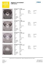
LED drivers Phosphor technology - Beriled
LED drivers Phosphor technology - Beriled
LED drivers Phosphor technology - Beriled

Create successful ePaper yourself
Turn your PDF publications into a flip-book with our unique Google optimized e-Paper software.
<strong>LED</strong> Lamps Require<br />
Integrated Power Conversion<br />
ICs To Meet EMC and Quality<br />
Standards<br />
> By Silvestro Fimiani, Power Integrations<br />
Regulatory standards in Europe and America are forcing the replacement<br />
of incandescent lamps with by more efficient lighting technologies such<br />
as compact fluorescent and <strong>LED</strong> bulbs. The recent introduction of more<br />
efficient high brightness white <strong>LED</strong>s (HB <strong>LED</strong>) has made this approach<br />
increasingly attractive. The most meaningful metric when comparing<br />
lighting technologies is luminous efficiency, which specifies the amount<br />
of light generated in the visible spectrum in lumens per watt of power<br />
supplied to the lamp. Incandescent and halogen bulbs are particularly<br />
poor in this regard, with efficiency ratings in the 15 to 20 Lm/W range.<br />
Compact fluorescent lamps are much better, with a typical value of 50<br />
Lm/W. However, within the past year, HB <strong>LED</strong>s have surpassed even this<br />
figure and are expected to reach values of up to 150 Lm/W by 2012. In<br />
addition to its greater energy efficiency the <strong>LED</strong> lamp has other<br />
significant advantages, including longer operating lifetime and lower<br />
operating and maintenance costs. Because of these factors the HB <strong>LED</strong><br />
lamp is expected to be a significant product for both residential and<br />
commercial usage for years to come.<br />
The fastest and easiest way to take advantage of this new lighting<br />
<strong>technology</strong> is through the retrofit market − replacing existing<br />
incandescent and halogen bulbs with HB <strong>LED</strong> lamps. The goal is to<br />
integrate both the HB <strong>LED</strong>s and their required drive electronics into a<br />
standard lamp housing such that it can be installed in an existing socket<br />
powered from the AC mains. The drive circuitry, or electronic ballast,<br />
provides the functions of line rectification, voltage reduction and<br />
generation of a regulated constant current to optimally power the <strong>LED</strong>s.<br />
Needless to say, the physical space constraints within the confines of<br />
the lamp housing create some difficult design challenges.<br />
Incandescent-replacement, retrofit <strong>LED</strong> lightbulbs have just recently<br />
started to be introduced, however they have suffered from several<br />
problems. Because it is tricky to fit the <strong>LED</strong> power driver circuitry into a<br />
standard bulb housing, some of these early <strong>LED</strong> lightbulbs have no<br />
internal filtering, so they will not pass EMC standards. Moreover, many<br />
of them use an inefficient capacitor dropper power supply rather than a<br />
switched-mode regulated ballast. This approach can cause a current<br />
unbalance on the AC mains which can create power quality problems in<br />
some installations. Both compliance with EMC regulations and power<br />
quality are important issues and must be considered.<br />
Recently, Power Integrations introduced its LinkSwitch TN family of<br />
power supply ICs in the tiny SO-8 package. This article describes a<br />
design for a high performance yet inexpensive electronic ballast for HB<br />
<strong>LED</strong> lamps using this chip that meets EN55022A EMI standards within<br />
the space limitations of standard lamp housings.<br />
Copyright © 2007 Luger Research & <strong>LED</strong> professional. All rights reserved.<br />
Design Objectives<br />
This design is intended to power a string of three HB <strong>LED</strong>s (the equivalent<br />
of a 10W standard incandescent lightbulb) with a nominal current of<br />
300 mA. In normal operation, the output voltage is clamped at about<br />
9.5 Vdc by the forward drop of the series <strong>LED</strong>s, but this circuit has a<br />
compliance of up to 12 Vdc to allow for variations in diode performance.<br />
The topology is a switched-mode constant current offline buck regulator,<br />
and is capable of operation over the entire 85 to 265 Vac universal input<br />
range and at line frequencies from 47 to 64 Hz. Other objectives include<br />
high efficiency, low cost, and compliance to EN55022A EMI requirements.<br />
The design can be integrated into a standard lamp housing - either<br />
screw-in Edison or bayonet halogen configurations - to allow for<br />
convenient retrofit within existing lamps. The design (Reference Design<br />
Kit 131), is fully supported with design tools and applications assistance<br />
in order to minimize time-to-market for new HB <strong>LED</strong> lamp products.<br />
EMI Considerations<br />
Power Integrations has found that many <strong>LED</strong> lightbulb designs on the<br />
market do not comply with conducted EMI specifications, due to both<br />
space and cost constraints. However, the design in this article takes<br />
advantage of the frequency jitter feature integrated into PI’s LinkSwitch-<br />
TN power conversion IC, which means that a smaller EMI filter can be<br />
used. .<br />
Design Details<br />
Power Integrations’ LinkSwitch®-TN LNK306DN integrated power<br />
conversion IC includes a fully integrated 700 V power MOSFET so that<br />
no external power device is required. The offline non-isolated buck<br />
topology operates at a maximum frequency of 66 KHz in continuous<br />
conduction mode. This frequency is modulated with a 4 kHz peak to<br />
peak frequency jitter to simplify the design requirements for the EMI<br />
filter. Although in this design a buck topology is used, this IC is also<br />
configurable as a buck-boost converter. Crucially, the LinkSwitch®-TN<br />
LNK306DN is in the compact SO-8 package - a major benefit to the<br />
mechanical design for this application.<br />
The schematic for both converter and EMI filter is shown in Figure 1.<br />
The current control loop is set to the desired constant current value<br />
based on the voltage drop across the current sensing resistors R8 and<br />
R10. While the nominal design is for a current of 300 mA, it can easily<br />
accommodate output currents of up to 360 mA. Q1 and Q2 amplify the<br />
sensed voltage drop such that a lower resistance current sensing resistor<br />
can be used for purposes of minimizing power dissipation. The EMI<br />
filter utilizes a pi topology and includes a fusible flameproof resistor,<br />
RF1, for overload protection.<br />
www.led-professional.com <strong>LED</strong> professional Review | June 2007 | page 35