
Create successful ePaper yourself
Turn your PDF publications into a flip-book with our unique Google optimized e-Paper software.
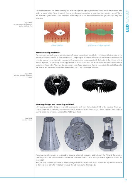
Figure 3.7.6:Air gaps between two surfaces: a)unfilled, b) filled <strong>by</strong> TIM.The most common is the white-colored paste or thermal grease, typically silicone oil filled with aluminum oxide, zincoxide, or boron nitride. Some brands of thermal interfaces use micronized or pulverized silver. Another type of TIM isthe phase-change materials. These are solid at room temperature but liquefy and behave like grease at operating temperatures.<strong>LED</strong> <strong>ACADEMY</strong>a) Interstitial air b) Thermal interface materialManufacturing methodsThe most common technique to take advantage of natural convection is to put holes in the top and bottom side of thehousing to allow for vertical air flow over the <strong>LED</strong>. Comparing an Aluminum die casting to an aluminum extrusion, theextrusion process inherently creates a product with greater density (less air voids inside the heat sink) than the die castingprocess (Figure 3.7.7). Assuming insulating properties of air and the conductive properties of aluminum, even the smallamounts of the air in the Aluminum die cast renders a significant reduction in thermal conductivity. Die-casted heatsinksare 20-30% less thermally conductive than extruded ones of the same shape and size.Figure 3.7.7:Heat sinks fabricated <strong>by</strong> extrusionmethod.Housing design and mounting method<strong>LED</strong> housings should be designed to provide a conductive path from the backside of PCB to the housing. This is typicallyaccomplished <strong>by</strong> mounting the backside of the PCB directly to the <strong>LED</strong> housing such that they are contacting oneanother across the entire rear surface of the PCB (Figure 3.7.8).Figure 3.7.8:Mounting method.This mounting scheme can be improved <strong>by</strong> applying a thermal conductive pad between the PCB and the housing.Thermally conductive pad conforms to the features on the backside of the PCB and provides a larger contact area forconduction.Also, the most common technique to take advantage of natural convection is to put holes in the top and bottom sideof the housing to allow for vertical air flow over the <strong>LED</strong> light source (Figure 3.7.8).19