NPN Silicon Push-Pull RF Power Transistor MRF392 - CB Tricks
NPN Silicon Push-Pull RF Power Transistor MRF392 - CB Tricks
NPN Silicon Push-Pull RF Power Transistor MRF392 - CB Tricks
- No tags were found...

You also want an ePaper? Increase the reach of your titles
YUMPU automatically turns print PDFs into web optimized ePapers that Google loves.
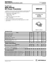
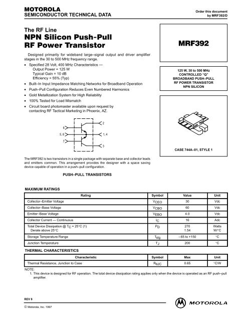
SEMICONDUCTOR TECHNICAL DATAOrder this documentby M<strong>RF</strong>392/DThe <strong>RF</strong> Line Designed primarily for wideband large–signal output and driver amplifierstages in the 30 to 500 MHz frequency range.• Specified 28 Volt, 400 MHz Characteristics —Output <strong>Power</strong> = 125 WTypical Gain = 10 dBEfficiency = 55% (Typ)• Built–In Input Impedance Matching Networks for Broadband Operation• <strong>Push</strong>–<strong>Pull</strong> Configuration Reduces Even Numbered Harmonics• Gold Metallization System for High Reliability• 100% Tested for Load Mismatch• Circuit board photomaster available upon request bycontacting <strong>RF</strong> Tactical Marketing in Phoenix, AZ.125 W, 30 to 500 MHzCONTROLLED “Q”BROADBAND PUSH–PULL<strong>RF</strong> POWER TRANSISTOR<strong>NPN</strong> SILICON65, 8721, 43CASE 744A–01, STYLE 1The M<strong>RF</strong>392 is two transistors in a single package with separate base and collector leadsand emitters common. This arrangement provides the designer with a space savingdevice capable of operation in a push–pull configuration.PUSH–PULL TRANSISTORSMAXIMUM RATINGSRating Symbol Value UnitCollector–Emitter Voltage VCEO 30 VdcCollector–Base Voltage V<strong>CB</strong>O 60 VdcEmitter–Base Voltage VEBO 4.0 VdcCollector Current — Continuous IC 16 AdcTotal Device Dissipation @ TC = 25°C (1)Derate above 25°CPD 2701.54Storage Temperature Range Tstg –65 to +150 °CJunction Temperature TJ 200 °CTHERMAL CHARACTERISTICSWattsW/°CCharacteristic Symbol Max UnitThermal Resistance, Junction to Case RθJC 0.65 °C/WNOTE:1. This device is designed for <strong>RF</strong> operation. The total device dissipation rating applies only when the device is operated as an <strong>RF</strong> push–pullamplifier.REV 8© MOTOROLA Motorola, Inc. 1997 <strong>RF</strong> DEVICE DATAM<strong>RF</strong>3921
ELECTRICAL CHARACTERISTICS (TC = 25°C unless otherwise noted)Characteristic Symbol Min Typ Max UnitOFF CHARACTERISTICS (1)Collector–Emitter Breakdown Voltage (IC = 50 mAdc, IB = 0) V(BR)CEO 30 — — VdcCollector–Emitter Breakdown Voltage (IC = 50 mAdc, VBE = 0) V(BR)CES 60 — — VdcEmitter–Base Breakdown Voltage (IE = 5.0 mAdc, IC = 0) V(BR)EBO 4.0 — — VdcCollector Cutoff Current (V<strong>CB</strong> = 30 Vdc, IE = 0) I<strong>CB</strong>O — — 5.0 mAdcON CHARACTERISTICS (1)DC Current Gain (IC = 1.0 Adc, VCE = 5.0 Vdc) hFE 40 60 100 —DYNAMIC CHARACTERISTICS (1)Output Capacitance (V<strong>CB</strong> = 28 Vdc, IE = 0, f = 1.0 MHz) Cob — 75 95 pFFUNCTIONAL TESTS (2) — See Figure 1Common–Emitter Amplifier <strong>Power</strong> Gain(VCC = 28 Vdc, Pout = 125 W, f = 400 MHz)Gpe 8.0 10 — dBCollector Efficiency(VCC = 28 Vdc, Pout = 125 W, f = 400 MHz)η 50 55 — %Load Mismatch(VCC = 28 Vdc, Pout = 125 W, f = 400 MHz,VSWR = 30:1, all phase angles)NOTES:1. Each transistor chip measured separately.2. Both transistor chips operating in push–pull amplifier.ψNo Degradation in Output <strong>Power</strong>C11L5+C12 C13 C14 C15+ 28 V–B1C1Z1Z2L1Z3Z4L3Z5Z6C9B2C3C4C5C6C7C8C2Z1Z2Z3L2D.U.T.Z4 Z5 Z6L4C10L6C16C17 C18 C19C1, C2 — 240 pF, 100 Mil Chip Cap (ATC) or EquivalentC3 — 3.6 pF, 100 Mil Chip Cap (ATC) or EquivalentC4, C8 — 8.2 pF, 100 Mil Chip Cap (ATC) or EquivalentC5, C6 — 20 pF, 100 Mil Chip Cap (ATC) or EquivalentC7 — 18 pF, Mini Unelco or EquivalentC9, C10 — 270 pF, 100 Mil Chip Cap (ATC) or EquivalentC11, C12, C16, C17 — 470 pF 100 Mil Chip Cap (ATC) or EquivalentC13, C18 — 680 pF FeedthruC14, C19 — 0.1 µF Erie Redcap or EquivalentC15 — 20 µF, 50 VL1, L2 — 0.15 µH Molded Choke With Ferrite BeadL3, L4 — 2–1/2 Turns #20 AWG, 0.200 IDL5, L6 — 3–1/2 Turns #18 AWG, 0.200 IDFigure 1. 400 MHz Test FixtureB1 — Balun, 50 Ω Semi–Rigid Coaxial Cable 86 Mil OD, 2″ LB2 — Balun, 50 Ω Semi–Rigid Coaxial Cable 86 Mil OD, 2″ LZ1 — Microstrip Line 270 Mil L x 125 Mil WZ2 — Microstrip Line 375 Mil L x 125 Mil WZ3 — Microstrip Line 280 Mil L x 125 Mil WZ4 — Microstrip Line 300 Mil L x 125 Mil WZ5 — Microstrip Line 350 Mil L x 125 Mil WZ6 — Microstrip Line 365 Mil L x 125 Mil WBoard Material — 0.0625″ Teflon Fiberglass εr = 2.5 ± 0.05 1 oz. Cu.Board Material — CLAD, Double SidedM<strong>RF</strong>3922MOTOROLA <strong>RF</strong> DEVICE DATA
P out , OUTPUT POWER (WATTS)16014012010080604020f = 100 MHz225 MHz400 MHz500 MHzVCC = 28 VP out , OUTPUT POWER (WATTS)8070605040302010f = 100 MHz225 MHz 400 MHzVCC = 13.5 V005 10 15 20 25Pin, INPUT POWER (WATTS)002 4 6 8 10 12 14 16 18 20Pin, INPUT POWER (WATTS)Figure 2. Output <strong>Power</strong> versus Input <strong>Power</strong>Figure 3. Output <strong>Power</strong> versus Input <strong>Power</strong>P out , OUTPUT POWER (WATTS)16014012010080604020Pin = 10 W7 W5 Wf = 225 MHzP out , OUTPUT POWER (WATTS)16014012010080604020Pin = 14 W10 W7 Wf = 400 MHz010 12 14 16 18 20 22 24 26 28 30VCC, SUPPLY VOLTAGE (VOLTS)Figure 4. Output <strong>Power</strong> versus Supply Voltage010 12 14 16 18 20 22 24 26 28 30VCC, SUPPLY VOLTAGE (VOLTS)Figure 5. Output <strong>Power</strong> versus Supply VoltageCAPACITIVEREACTANCECOMPONENT (–jX)Zo = 20 ΩZOL*225f = 100 MHzf = 100 MHz400500450500fMHz100225400450500225450Zin400VCC = 28 V, Pout = 125 WZinOHMS0.72 + j0.440.72 + j2.623.88 + j5.723.84 + j2.81.26 + j3.01INDUCTIVEREACTANCECOMPONENT (+jX)ZOL*OHMSZOL* = Conjugate of the optimum load impedanceZOL* = into which the device output operates at aZOL* = given output power, voltage and frequency.Zin & ZOL* are givenfrom base–to–base andcollector–to–collector respectively.9.0 – j6.05.2 – j1.83.6 + j0.533.2 + j1.23.0 + j2.0Figure 6. Series Equivalent Input/Output ImpedanceMOTOROLA <strong>RF</strong> DEVICE DATAM<strong>RF</strong>3923
PACKAGE DIMENSIONSU 4 PLQ0.76 (0.030) M A M B MRD 4 PLJHM1 2 3 45 6 7 8LG–A–NK–B–KF 4 PLV 2 PLCE–T–SEATINGPLANENOTES:1. DIMENSIONING AND TOLERANCING PER ANSIY14.5M, 1982.STYLE 1:PIN 1. EMITTER (COMMON)2. COLLECTOR3. COLLECTOR4. EMITTER (COMMON)5. EMITTER (COMMON)6. BASE7. BASE8. EMITTER (COMMON)MILLIMETERS INCHESDIM MIN MAX MIN MAXA 22.60 23.11 0.890 0.910B 9.52 10.03 0.375 0.395C 6.65 7.16 0.262 0.282D 1.60 1.95 0.063 0.077E 2.94 3.40 0.116 0.134F 2.87 3.22 0.113 0.127G 16.51 BSC 0.650 BSCH 4.01 4.36 0.158 0.172J 0.07 0.15 0.003 0.006K 4.34 4.90 0.171 0.193L 12.45 12.95 0.490 0.510M 45 NOM 45 NOMN 1.051 11.02 0.414 0.434Q 3.04 3.35 0.120 0.132R 9.90 10.41 0.390 0.410U 1.02 1.27 0.040 0.050V 0.64 0.89 0.025 0.035CASE 744A–01ISSUE CMotorola reserves the right to make changes without further notice to any products herein. Motorola makes no warranty, representation or guarantee regardingthe suitability of its products for any particular purpose, nor does Motorola assume any liability arising out of the application or use of any product or circuit,and specifically disclaims any and all liability, including without limitation consequential or incidental damages. “Typical” parameters can and do vary in differentapplications. All operating parameters, including “Typicals” must be validated for each customer application by customer’s technical experts. Motorola doesnot convey any license under its patent rights nor the rights of others. Motorola products are not designed, intended, or authorized for use as components insystems intended for surgical implant into the body, or other applications intended to support or sustain life, or for any other application in which the failure ofthe Motorola product could create a situation where personal injury or death may occur. Should Buyer purchase or use Motorola products for any suchunintended or unauthorized application, Buyer shall indemnify and hold Motorola and its officers, employees, subsidiaries, affiliates, and distributors harmlessagainst all claims, costs, damages, and expenses, and reasonable attorney fees arising out of, directly or indirectly, any claim of personal injury or deathassociated with such unintended or unauthorized use, even if such claim alleges that Motorola was negligent regarding the design or manufacture of the part.Motorola and are registered trademarks of Motorola, Inc. Motorola, Inc. is an Equal Opportunity/Affirmative Action Employer.How to reach us:USA / EUROPE: Motorola Literature Distribution;JAPAN: Nippon Motorola Ltd.; Tatsumi–SPD–JLDC, Toshikatsu Otsuki,P.O. Box 20912; Phoenix, Arizona 85036. 1–800–441–2447 6F Seibu–Butsuryu–Center, 3–14–2 Tatsumi Koto–Ku, Tokyo 135, Japan. 03–3521–8315MFAX: RMFAX0@email.sps.mot.com – TOUCHTONE (602) 244–6609 HONG KONG: Motorola Semiconductors H.K. Ltd.; 8B Tai Ping Industrial Park,INTERNET: http://Design–NET.com 51 Ting Kok Road, Tai Po, N.T., Hong Kong. 852–26629298M<strong>RF</strong>3924◊MOTOROLA <strong>RF</strong> DEVICE M<strong>RF</strong>392/D DATA