SANYO Electric Co.,Ltd. Semiconductor Bussiness Headquarters
SANYO Electric Co.,Ltd. Semiconductor Bussiness Headquarters
SANYO Electric Co.,Ltd. Semiconductor Bussiness Headquarters

Create successful ePaper yourself
Turn your PDF publications into a flip-book with our unique Google optimized e-Paper software.
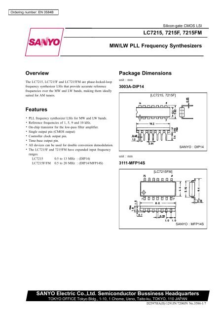
Ordering number: EN 3584BSilicon-gate CMOS LSILC7215, 7215F, 7215FMMW/LW PLL Frequency SynthesizersOverviewThe LC7215, LC7215F and LC7215FM are phase-locked-loopfrequency synthesizer LSIs that provide accurate referencefrequencies over the MW and LW bands, making them ideallysuited for AM tuners.Package Dimensionsunit : mm3003A-DIP14[LC7215, 7215F]FeaturesPLL frequency synthesizer LSIs for MW and LW bands.Reference frequencies of 1, 5, 9 and 10 kHz.On-chip transistor for the low-pass filter amplifier.Single output pin (CMOS output)<strong>Co</strong>ntroller clock output pin.Time-base output pin..All devices can be used for double conversion demodulation.The LC7215F and 7215FM have expanded input frequencyranges.LC7215 0.5 to 13 MHz : (DIP14)LC7215F/FM 0.5 to 20 MHz : (DIP14/MFP14S)unit : mm3111-MFP14S<strong>SANYO</strong> : DIP14[LC7215FM]<strong>SANYO</strong> : MFP14S<strong>SANYO</strong> <strong>Electric</strong> <strong>Co</strong>.,<strong>Ltd</strong>. <strong>Semiconductor</strong> <strong>Bussiness</strong> <strong>Headquarters</strong>TOKYO OFFICE Tokyo Bldg., 1-10, 1 Chome, Ueno, Taito-ku, TOKYO, 110 JAPAND2597HA(II)/1291JN/7200JN No.3584-1/7
LC7215, 7215F, 7215FMSpecificationsAbsolute Maximum Ratings at Ta = 25°C, V SS =0VValues in parentheses are for the LC7215F and LC7215FM.Parameter Symbol <strong>Co</strong>nditions Ratings UnitMaximum supply voltage V DD max V DD –0.3 to +6.5 VInput voltage V IN 1 All input pins –0.3 to V DD +0.3 VV IN 2 CE, CL, DATA (Note) –0.3 to +6.5 VOutput current I OUT AOUT 0 to 5 mAOutput voltage V OUT 1 AOUT –0.3 to +15 VV OUT 2 SYC, TB –0.3 to +6.5 VV OUT 3 All output pins except V OUT 1 and V OUT 2 –0.3 to V DD +0.3 VAllowable powerdissipationPd max Ta % 85°C 150 mWOperating temperature Topr –40 to +85 °CStorage temperature Tstg –55 to +125 °CNote: Voltage that is applied to the resistors when resistors totaling at least 10 kΩ are connected to a pin in series.Allowable Operating <strong>Co</strong>nditions at V SS =0VValues in parentheses are for the LC7215F and LC7215FM.Parameter Symbol <strong>Co</strong>nditions min typ max UnitSupply voltageV DD 1 V DD (4.5)3.0 (5.5)5.5 VV DD 2 V DD (Crystal OSC oscillation guaranteed) 3.0 5.5 VHigh-level input voltage V IH CE, CL, DATA 2.0 V DD 1 VLow-level input voltage V IL CE, CL, DATA 0 0.5 VOutput voltageV OUT 1 AOUT 13 VV OUT 2 SYC, TB 5.5 VInput frequencyPIN: Sine wave, capacitive coupling Vf IN 1DD 1,*S =1(2.3)2.3 (20)13 MHzPIN: Sine wave, capacitive coupling Vf IN 2DD 1,*S =00.5 2.5 MHzOscillation guaranteedcrystal oscillatorX’tal XIN, XOUT: CI % 30 Ω 8.00 11.16 12.00 MHzInput amplitudePIN: Square wave, capacity connection VV IN 1DD 1,*S =1100 1000 mVrmsPIN: Square wave, capacity connection VV IN 2DD 1,*S =0100 1000 mVrmsPower supply —V DD ,V SS : A capacitor of at least 1000 pFmust be inserted.1000 pFNo.3584-2/7
LC7215, 7215F, 7215FM<strong>Electric</strong>al Characteristics within the allowable operating rangesValues in parentheses are for LC7215F and LC7215FM.Parameter Symbol <strong>Co</strong>nditions min typ max UnitI IH 1 XIN: V I =V DD 20 µAHigh-level input currentsI IH 2 PIN: V I =V DD 40 µAI IH 3 CE, CL, DATA: V I =V DD 3.0 µAI IH 4 AIN: V I =V DD 0.01 1.0 µAI IL 1 XIN: V I =V SS 20 µALow-level input currentsI IL 2 PIN: V I =V SS 40 µAI IL 3 CE, CL, DATA: V I =V SS 3.0 µAI IL 4 AIN: V I =V SS 0.01 1.0 µAHigh-level output voltagesLow-level output voltagesOutput off-state leakagecurrentsTristate output High-leveloff-state leakage currentTristate output Low-leveloff-state leakage currentVV OH 1 DOUT: I O =1mADD–1.0VVV OH 2 PDOUT: I O = 0.5 mADD–1.0VV OL 1 DOUT: I O = –1 mA 1.0 VV OL 2 PDOUT: I O = –0.5 mA 1.0 VV OL 4 SYC, TB: I O = 0.5 mA 1.0 VV OL 5 AOUT: I O = 1 mA 1.0 VI OFF 1 SYC, TB: V O =V DD 3.0 µAI OFF 2 AOUT: V O = 13 V 5.0 µAI OFF H PDOUT: V O =V DD 0.01 1.0 nAI OFF L PDOUT: V O =V SS 0.01 1.0 nAVHigh-level output voltage V OH 3 XOUT: I O = –0.1 mADD–1.0VLow-level output voltage V OL 3 XOUT: I O = 0.1 mA 1.0 VI DD 1V DD :f IN 1 = 13 MHz, *S = 1 (High speed)(Note 1)10 mAf IN 1 = 20 MHz, *S = 1 (High speed)(Note 1)(12) mASupply currentVI DD 2 DD :f IN 1 = 2.5 MHz, *S = 0 (Low speed)(Note 1)5 mAV DD :V DD = 5.5 V, *O = 0, P = 1 (Note 2) 1.2 2.0 mAI DD 3V DD = 4.5 V, *O = 0, P = 1 (Note 2) 0.7 1.5 mAV DD = 3.0 V, *O = 0, P = 1 (Note 2) 0.4 1.0 mA* S, O and P are serial control bits.Note 1. V IN 1=V IN 2 = 100 mVms. The 11.16 MHz crystal is connected to XIN and XOUT. All other inputs are connected to V SSand all other outputs are open.2. The 11.16 MHz crystal is connected to XIN and XOUT. All other inputs are connected to V DD and all other outputs areopen. (Backup mode when PLL is halted.)Pin AssignmentNo.3584-3/7
LC7215, 7215F, 7215FMBlock DiagramPin DescriptionNameXIN, XOUTPINV DD ,V SSDATA, CL, CEDOUTAIN, AOUTPDOUTTBSYCDescription11.16 MHz crystal oscillator connection, feedbackresistance built-inLocal oscillator signal inputPower supplyData inputSingle bit data outputLow-pass filter amplifierCharge pump output8 Hz time-base output60 kHz controller clock outputNo.3584-4/7
LC7215, 7215F, 7215FMData InputInternaldata(1) A to N: Divider dataInput MSB firstExample:Division by 12,420(2) O, P: Mode selectionMode O P DOUT TB OperationNOR1 0 0 T 8 Hz Normal operation (with PLL operating)NOR2 0 1 T 8 Hz Normal operation (backup when PLL is halted)TEST1 1 0 (Device test mode)TEST2 1 1 (Device test mode)(3) Q, R: Reference frequency selectionQ R Reference frequency0 0 9 kHz0 1 10 kHz1 0 1 kHz1 1 5 kHz(4) S: Programmable divider input sensitivity switchS = 1: for High speedS = 0: for Low speed(5) T: Output to DOUTT = 1: DOUT = 1T = 0: DOUT = 0No.3584-5/7
LC7215, 7215F, 7215FMData Input TimingV IH = 2.0 to V DD ,V IL =0to0.5VX’tal = 8.00 to 11.16 (typ) to 12.00 MHzData latch: Rising edge of CLItem Symbol 11.16 MHz crystal Other crystal frequencies Effective valueEnable setup time t ES At least 12 µs At least 2 × (1/fXtal × 62)Enable hold time t EH ↑ ↑Data setup time t SU ↑ ↑Data hold time t HD ↑ ↑Clock Low-level time t LO ↑ ↑Clock High-level time t HI ↑ ↑Rise time t R 1 µs or less 1 µs or lessFall time t F ↑ ↑1/2 of the valueshown at leftNo.3584-6/7
LC7215, 7215F, 7215FM(1) Sample Application Circuit(2) Double-conversion ReceiverNo products described or contained herein are intended for use in surgical implants, life-support systems,aerospace equipment, nuclear power control systems, vehicles, disaster/crime-prevention equipment and the like,the failure of which may directly or indirectly cause injury, death or property loss.Anyone purchasing any products described or contained herein for an above-mentioned use shall:1 Accept full responsibility and indemnify and defend <strong>SANYO</strong> ELECTRIC CO., LTD., its affiliates, subsidiaries anddistributors and all their officers and employees, jointly and severally, against any and all claims and litigationand all damages, cost and expenses associated with such use:2 Not impose any responsibility for any fault or negligence which may be cited in any such claim or litigation on<strong>SANYO</strong> ELECTRIC CO., LTD., its affiliates, subsidiaries and distributors or any of their officers and employeesjointly or severally.Information (including circuit diagrams and circuit parameters) herein is for example only; it is not guaranteed forvolume production. <strong>SANYO</strong> believes information herein is accurate and reliable, but no guarantees are made orimplied regarding its use or any infringements of intellectual property rights or other rights of third parties.This catalog provides information as of December, 1997. Specifications and information herein are subject to change without notice.No.3584-7/7