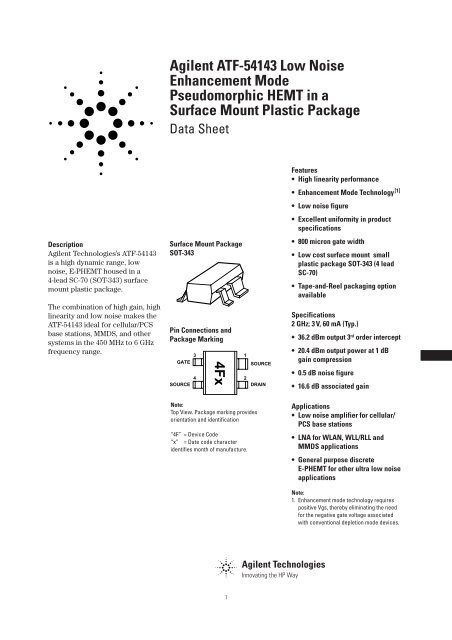
Agilent ATF-54143 Low Noise Enhancement Mode ... - Ok2kkw.com
Agilent ATF-54143 Low Noise Enhancement Mode ... - Ok2kkw.com
Agilent ATF-54143 Low Noise Enhancement Mode ... - Ok2kkw.com

Create successful ePaper yourself
Turn your PDF publications into a flip-book with our unique Google optimized e-Paper software.
<strong>ATF</strong>-<strong>54143</strong> Typical Performance Curves, continued221942201837P1dB (dBm)181614GAIN (dB)171615OIP3 (dBm)3227121422103V 60 mA133V4V173V4V80 1 2 3 4 5 6FREQUENCY (GHz)Figure 9. P1dB vs. Frequency and BiasTuned for Max OIP3 and Fmin at 2 GHz.120 20 40 60 80 100I d (mA)Figure 10. Gain vs. I ds and V ds Tuned forMax OIP3 and Fmin at 2 GHz.120 20 40 60 80 100I d (mA)Figure 11. OIP3 vs. I ds and V ds Tuned forMax OIP3 and Fmin at 2 GHz.242540222435P1dB (dBm)201816143V4VGAIN (dB)23222120193V4VOIP3 (dBm)3025203V4V120 20 40 60 80 100I d (mA)Figure 12. P1dB vs. I ds and V ds Tuned forMax OIP3 and Fmin at 2 GHz.180 20 40 60 80 100I d (mA)Figure 13. Gain vs. I ds and V ds Tuned forMax OIP3 and Fmin at 900 MHz.150 20 40 60 80 100I d (mA)Figure 14. OIP3 vs. I ds and V ds Tuned forMax OIP3 and Fmin at 900 MHz.P1dB (dBm)23222120191817163V4VGAIN (dB)35302520151025°C-40°C85°CFmin (dB)21.51.00.525°C-40°C85°C150 20 40 60 80 100I dq (mA) [1]Figure 15. P1dB vs. I ds and V ds Tuned forMax OIP3 and Fmin at 900 MHz.50 1 2 3 4 5 6FREQUENCY (GHz)Figure 16. Gain vs. Frequency and TempTuned for Max OIP3 and Fmin at 3V, 60 mA.00 1 2 3 4 5 6FREQUENCY (GHz)Figure 17. Fmin vs. Frequency and TempTuned for Max OIP3 and Fmin at 3V, 60 mA.Note:1. I dq represents the quiescent drain currentwithout RF drive applied. Under low valuesof I dq , the application of RF drive will causeI d to increase substantially as P1dB isapproached.
<strong>ATF</strong>-<strong>54143</strong> Typical Performance Curves, continued4521402.0OIP3 (dBm)403530252015FREQUENCY (GHz)25°C-40°C85°C10170 1 2 3 4 5 6 0 1 2 3 4 5 6Figure 18. OIP3 vs. Frequency and TempTuned for Max OIP3 and Fmin at 3V, 60 mA.P1dB (dBm)20.52019.51918.51817.525°C-40°C85°CFREQUENCY (GHz)Figure 19. P1dB vs. Frequency and TempTuned for Max OIP3 and Fmin at 3V, 60 mA.GAIN (dB), OIP3 & P1dB (dBm)3020100OIP3P1dBGainNF0.500 20 40 60 80 100I d (mA)Figure 20. OIP3, P1dB, Gain and Fmin vs.I ds at 3V @ 2 GHz.1.51.0Fmin (dB)402.0401401GAIN (dB), OIP3 & P1dB (dBm)3020100OIP3P1dBGainNF0.500 20 40 60 80 100I d (mA)Figure 21. OIP3, P1dB, Gain and Fmin vs.I ds at 4V @ 2 GHz.1.51.0Fmin (dB)GAIN (dB), OIP3 & P1dB (dBm)302010OIP3 0.20P1dBGainNF00 20 40 60 80 100I d (mA)Figure 22. OIP3, P1dB, Gain and Fmin vs.I ds at 3V @ 900 MHz.0.80.60.4Fmin (dB)GAIN (dB), OIP3 & P1dB (dBm)302010OIP3 0.20P1dBGainNF00 20 40 60 80 100I d (mA)Figure 23. OIP3, P1dB, Gain and Fmin vs.I ds at 4V @ 900 MHz.0.80.60.4Fmin (dB)Fmin (dB)1.41.21.00.80.60.40.260 mA40 mA80 mA00 1 2 3 4 5 6 7FREQUENCY (GHz)<strong>ATF</strong>-<strong>54143</strong> Reflection Coefficient Parameters tuned for Maximum Output IP3,V DS = 3V, I DS = 60 mAFreq ΓOut_Mag. [1] ΓOut_Ang. [1] OIP3 P1dB(GHz) (Mag) (Degrees) (dBm) (dBm)0.9 0.017 115 35.54 18.42.0 0.026 -85 36.23 20.383.9 0.013 173 37.54 20.285.8 0.025 102 35.75 18.09Note:1. Gamma out is the reflection coefficient of the matching circuit presented to the output of the device.Figure 24. Fmin [1] vs. Frequency and I dsat 3V.Note:1. Fmin values at 2 GHz and higher are basedon measurements while the Fmins below2 GHz have been extrapolated. The Fminvalues are based on a set of 16 noise figuremeasurements made at 16 differentimpedances using an ATN NP5 test system.From these measurements a true Fmin iscalculated. Refer to the noise parameterapplication section for more information.
<strong>ATF</strong>-<strong>54143</strong> Typical Scattering Parameters, V DS = 3 V, I DS = 40 mAFreq. S 11 S 21 S 12 S 22 MSG/MAGGHz Mag. Ang. dB Mag. Ang. Mag. Ang. Mag. Ang.0.1 0.99 -17.6 27.99 25.09 168.5 0.009 80.2 0.59 -12.8 34.450.5 0.83 -76.9 25.47 18.77 130.1 0.036 52.4 0.44 -54.6 27.170.9 0.72 -114 22.52 13.37 108 0.047 40.4 0.33 -78.7 24.541.0 0.70 -120.6 21.86 12.39 103.9 0.049 38.7 0.31 -83.2 24.031.5 0.65 -146.5 19.09 9.01 87.4 0.057 33.3 0.24 -99.5 21.991.9 0.63 -162.1 17.38 7.40 76.6 0.063 30.4 0.20 -108.6 20.702.0 0.62 -165.6 17.00 7.08 74.2 0.065 29.8 0.19 -110.9 20.372.5 0.61 178.5 15.33 5.84 62.6 0.072 26.6 0.15 -122.6 19.093.0 0.61 164.2 13.91 4.96 51.5 0.080 22.9 0.12 -137.5 17.924.0 0.63 138.4 11.59 3.80 31 0.094 14 0.10 176.5 16.065.0 0.66 116.5 9.65 3.04 11.6 0.106 4.2 0.14 138.4 14.576.0 0.69 97.9 8.01 2.51 -6.7 0.118 -6.1 0.17 117.6 13.287.0 0.71 80.8 6.64 2.15 -24.5 0.128 -17.6 0.20 98.6 12.258.0 0.72 62.6 5.38 1.86 -42.5 0.134 -29.3 0.22 73.4 11.429.0 0.76 45.2 4.20 1.62 -60.8 0.145 -40.6 0.27 52.8 10.4810.0 0.83 28.2 2.84 1.39 -79.8 0.150 -56.1 0.37 38.3 9.6611.0 0.85 13.9 1.42 1.18 -96.9 0.149 -69.3 0.45 25.8 8.9812.0 0.88 -0.5 0.23 1.03 -112.4 0.150 -81.6 0.51 12.7 8.3513.0 0.89 -15.1 -0.86 0.91 -129.7 0.149 -95.7 0.54 -4.1 7.8414.0 0.87 -31.6 -2.18 0.78 -148 0.143 -110.3 0.61 -20.1 7.3615.0 0.88 -46.1 -3.85 0.64 -164.8 0.132 -124 0.65 -34.9 6.8716.0 0.87 -54.8 -5.61 0.52 -178.4 0.121 -134.6 0.70 -45.6 6.3717.0 0.87 -62.8 -7.09 0.44 170.1 0.116 -144.1 0.73 -55.9 5.8118.0 0.92 -73.6 -8.34 0.38 156.1 0.109 -157.4 0.76 -68.7 5.46Typical <strong>Noise</strong> Parameters, V DS = 3 V, I DS = 40 mAFreq F min Γ opt Γ opt R n/50 G aGHz dB Mag. Ang. dB0.5 0.17 0.34 34.80 0.04 27.830.9 0.22 0.32 53.00 0.04 23.571.0 0.24 0.32 60.50 0.04 22.931.9 0.42 0.29 108.10 0.04 18.352.0 0.45 0.29 111.10 0.04 17.912.4 0.51 0.30 136.00 0.04 16.393.0 0.59 0.32 169.90 0.05 15.403.9 0.69 0.34 -151.60 0.05 13.265.0 0.90 0.45 -119.50 0.09 11.895.8 1.14 0.50 -101.60 0.16 10.956.0 1.17 0.52 -99.60 0.18 10.647.0 1.24 0.58 -79.50 0.33 9.618.0 1.57 0.60 -57.90 0.56 8.369.0 1.64 0.69 -39.70 0.87 7.7710.0 1.8 0.80 -22.20 1.34 7.68MSG/MAG and S21 (dB)403530252015MSG105S021-510-150 5 10 15 20FREQUENCY (GHz)Figure 25. MSG/MAG and |S 21 | 2 vs. Frequencyat 3V, 40 mA.Notes:1. F min values at 2 GHz and higher are based on measurements while the F mins below 2 GHz have been extrapolated. The F min values are based on aset of 16 noise figure measurements made at 16 different impedances using an ATN NP5 test system. From these measurements a true F min iscalculated. Refer to the noise parameter application section for more information.2. S and noise parameters are measured on a microstrip line made on 0.025 inch thick alumina carrier. The input reference plane is at the end of thegate lead. The output reference plane is at the end of the drain lead. The parameters include the effect of four plated through via holes connectingsource landing pads on top of the test carrier to the microstrip ground plane on the bottom side of the carrier. Two 0.020 inch diameter via holes areplaced within 0.010 inch from each source lead contact point, one via on each side of that point.
<strong>ATF</strong>-<strong>54143</strong> Typical Scattering Parameters, V DS = 3V, I DS = 60 mAFreq. S 11 S 21 S 12 S 22 MSG/MAGGHz Mag. Ang. dB Mag. Ang. Mag. Ang. Mag. Ang.0.1 0.99 -18.9 28.84 27.66 167.6 0.01 80.0 0.54 -14.0 34.880.5 0.81 -80.8 26.04 20.05 128.0 0.03 52.4 0.40 -58.8 27.840.9 0.71 -117.9 22.93 14.01 106.2 0.04 41.8 0.29 -83.8 25.131.0 0.69 -124.4 22.24 12.94 102.2 0.05 40.4 0.27 -88.5 24.591.5 0.64 -149.8 19.40 9.34 86.1 0.05 36.1 0.21 -105.2 22.461.9 0.62 -164.9 17.66 7.64 75.6 0.06 33.8 0.17 -114.7 21.052.0 0.62 -168.3 17.28 7.31 73.3 0.06 33.3 0.17 -117.0 20.712.5 0.60 176.2 15.58 6.01 61.8 0.07 30.1 0.13 -129.7 19.343.0 0.60 162.3 14.15 5.10 51.0 0.08 26.5 0.11 -146.5 18.154.0 0.62 137.1 11.81 3.90 30.8 0.09 17.1 0.10 165.2 16.175.0 0.66 115.5 9.87 3.11 11.7 0.11 6.8 0.14 131.5 14.646.0 0.69 97.2 8.22 2.58 -6.4 0.12 -3.9 0.18 112.4 13.367.0 0.70 80.2 6.85 2.20 -24.0 0.13 -15.8 0.20 94.3 12.298.0 0.72 62.2 5.58 1.90 -41.8 0.14 -28.0 0.23 70.1 11.459.0 0.76 45.0 4.40 1.66 -59.9 0.15 -39.6 0.29 50.6 10.5310.0 0.83 28.4 3.06 1.42 -78.7 0.15 -55.1 0.38 36.8 9.7111.0 0.85 13.9 1.60 1.20 -95.8 0.15 -68.6 0.46 24.4 9.0412.0 0.88 -0.2 0.43 1.05 -111.1 0.15 -80.9 0.51 11.3 8.4313.0 0.89 -14.6 -0.65 0.93 -128.0 0.15 -94.9 0.55 -5.2 7.9414.0 0.88 -30.6 -1.98 0.80 -146.1 0.14 -109.3 0.61 -20.8 7.4315.0 0.88 -45.0 -3.62 0.66 -162.7 0.13 -122.9 0.66 -35.0 6.9816.0 0.88 -54.5 -5.37 0.54 -176.6 0.12 -133.7 0.70 -45.8 6.4917.0 0.88 -62.5 -6.83 0.46 171.9 0.12 -143.2 0.73 -56.1 5.9518.0 0.92 -73.4 -8.01 0.40 157.9 0.11 -156.3 0.76 -68.4 5.66Typical <strong>Noise</strong> Parameters, V DS = 3V, I DS = 60 mAFreq F min Γ opt Γ opt R n/50 G aGHz dB Mag. Ang. dB0.5 0.15 0.34 42.3 0.04 28.500.9 0.20 0.32 62.8 0.04 24.181.0 0.22 0.32 67.6 0.04 23.471.9 0.42 0.27 116.3 0.04 18.672.0 0.45 0.27 120.1 0.04 18.292.4 0.52 0.26 145.8 0.04 16.653.0 0.59 0.29 178.0 0.05 15.563.9 0.70 0.36 -145.4 0.05 13.535.0 0.93 0.47 -116.0 0.10 12.135.8 1.16 0.52 -98.9 0.18 11.106.0 1.19 0.55 -96.5 0.20 10.957.0 1.26 0.60 -77.1 0.37 9.738.0 1.63 0.62 -56.1 0.62 8.569.0 1.69 0.70 -38.5 0.95 7.9710.0 1.73 0.79 -21.5 1.45 7.76MSG/MAG and S21 (dB)403530252015MSG105S021-510-150 5 10 15 20FREQUENCY (GHz)Figure 26. MSG/MAG and |S 21 | 2 vs. Frequencyat 3V, 60 mA.Notes:1. F min values at 2 GHz and higher are based on measurements while the F mins below 2 GHz have been extrapolated. The F min values are based on aset of 16 noise figure measurements made at 16 different impedances using an ATN NP5 test system. From these measurements a true F min iscalculated. Refer to the noise parameter application section for more information.2. S and noise parameters are measured on a microstrip line made on 0.025 inch thick alumina carrier. The input reference plane is at the end of thegate lead. The output reference plane is at the end of the drain lead. The parameters include the effect of four plated through via holes connectingsource landing pads on top of the test carrier to the microstrip ground plane on the bottom side of the carrier. Two 0.020 inch diameter via holes areplaced within 0.010 inch from each source lead contact point, one via on each side of that point.
<strong>ATF</strong>-<strong>54143</strong> Typical Scattering Parameters, V DS = 3V, I DS = 80 mAFreq. S 11 S 21 S 12 S 22 MSG/MAGGHz Mag. Ang. dB Mag. Ang. Mag. Ang. Mag. Ang.0.1 0.98 -20.4 28.32 26.05 167.1 0.01 79.4 0.26 -27.6 34.160.5 0.80 -85.9 25.32 18.45 126.8 0.04 53.3 0.29 -104.9 27.100.9 0.72 -123.4 22.10 12.73 105.2 0.05 43.9 0.30 -138.8 24.151.0 0.70 -129.9 21.40 11.75 101.3 0.05 42.7 0.30 -144.3 23.631.5 0.66 -154.6 18.55 8.46 85.4 0.06 38.6 0.30 -165.0 21.351.9 0.65 -169.5 16.81 6.92 74.9 0.07 35.7 0.29 -177.6 19.892.0 0.64 -172.8 16.42 6.62 72.6 0.07 35.0 0.29 179.4 19.522.5 0.64 172.1 14.69 5.42 61.1 0.09 30.6 0.29 164.4 18.053.0 0.63 158.5 13.24 4.59 50.1 0.10 25.5 0.29 150.2 16.804.0 0.66 133.8 10.81 3.47 29.9 0.12 13.4 0.33 126.1 14.765.0 0.69 112.5 8.74 2.74 11.1 0.13 1.2 0.39 107.8 13.206.0 0.72 94.3 7.03 2.25 -6.5 0.14 -11.3 0.42 91.8 11.967.0 0.73 77.4 5.63 1.91 -23.5 0.15 -24.5 0.44 75.5 10.978.0 0.74 59.4 4.26 1.63 -41.1 0.16 -38.1 0.47 55.5 10.149.0 0.78 42.1 2.98 1.41 -58.7 0.17 -51.1 0.52 37.8 9.3210.0 0.84 25.6 1.51 1.19 -76.4 0.16 -66.8 0.59 24.0 8.6011.0 0.86 11.4 0.00 1.00 -92.0 0.16 -79.8 0.64 11.8 8.0412.0 0.88 -2.6 -1.15 0.88 -105.9 0.16 -91.7 0.68 -0.8 7.5213.0 0.89 -17.0 -2.18 0.78 -121.7 0.15 -105.6 0.70 -16.7 7.1214.0 0.87 -33.3 -3.48 0.67 -138.7 0.14 -119.5 0.73 -31.7 6.7715.0 0.87 -47.3 -5.02 0.56 -153.9 0.13 -132.3 0.76 -44.9 6.4216.0 0.86 -55.6 -6.65 0.47 -165.9 0.12 -141.7 0.78 -54.9 5.9917.0 0.86 -63.4 -7.92 0.40 -175.9 0.11 -150.4 0.79 -64.2 5.5518.0 0.91 -74.2 -8.92 0.36 171.2 0.10 -163.0 0.81 -76.2 5.37Typical <strong>Noise</strong> Parameters, V DS = 3V, I DS = 80 mAFreq F min Γ opt Γ opt R n/50 G aGHz dB Mag. Ang. dB0.5 0.19 0.23 66.9 0.04 27.930.9 0.24 0.24 84.3 0.04 24.131.0 0.25 0.25 87.3 0.04 23.301.9 0.43 0.28 134.8 0.04 18.552.0 0.42 0.29 138.8 0.04 18.152.4 0.51 0.30 159.5 0.03 16.443.0 0.61 0.35 -173 0.03 15.133.9 0.70 0.41 -141.6 0.06 12.975.0 0.94 0.52 -113.5 0.13 11.425.8 1.20 0.56 -97.1 0.23 10.486.0 1.26 0.58 -94.8 0.26 10.117.0 1.34 0.62 -75.8 0.46 8.868.0 1.74 0.63 -55.5 0.76 7.599.0 1.82 0.71 -37.7 1.17 6.9710.0 1.94 0.79 -20.8 1.74 6.65MSG/MAG and S21 (dB)403530252015MSG1050S 21-510-150 5 10 15 20FREQUENCY (GHz)Figure 27. MSG/MAG and |S 21 | 2 vs. Frequencyat 3V, 80 mA.Notes:1. F min values at 2 GHz and higher are based on measurements while the F mins below 2 GHz have been extrapolated. The F min values are based on aset of 16 noise figure measurements made at 16 different impedances using an ATN NP5 test system. From these measurements a true F min iscalculated. Refer to the noise parameter application section for more information.2. S and noise parameters are measured on a microstrip line made on 0.025 inch thick alumina carrier. The input reference plane is at the end of thegate lead. The output reference plane is at the end of the drain lead. The parameters include the effect of four plated through via holes connectingsource landing pads on top of the test carrier to the microstrip ground plane on the bottom side of the carrier. Two 0.020 inch diameter via holes areplaced within 0.010 inch from each source lead contact point, one via on each side of that point.
<strong>ATF</strong>-<strong>54143</strong> Typical Scattering Parameters, V DS = 4V, I DS = 60 mAFreq. S 11 S 21 S 12 S 22 MSG/MAGGHz Mag. Ang. dB Mag. Ang. Mag. Ang. Mag. Ang.0.1 0.99 -18.6 28.88 27.80 167.8 0.01 80.1 0.58 -12.6 35.410.5 0.81 -80.2 26.11 20.22 128.3 0.03 52.4 0.42 -52.3 28.140.9 0.71 -117.3 23.01 14.15 106.4 0.04 41.7 0.31 -73.3 25.381.0 0.69 -123.8 22.33 13.07 102.4 0.04 40.2 0.29 -76.9 24.831.5 0.64 -149.2 19.49 9.43 86.2 0.05 36.1 0.22 -89.4 22.751.9 0.62 -164.5 17.75 7.72 75.7 0.06 34.0 0.18 -95.5 21.322.0 0.61 -167.8 17.36 7.38 73.3 0.06 33.5 0.18 -97.0 21.042.5 0.60 176.6 15.66 6.07 61.9 0.07 30.7 0.14 -104.0 19.643.0 0.60 162.6 14.23 5.15 51.1 0.07 27.3 0.11 -113.4 18.484.0 0.62 137.4 11.91 3.94 30.9 0.09 18.7 0.07 -154.7 16.465.0 0.65 115.9 10.00 3.16 11.7 0.10 9.0 0.09 152.5 14.966.0 0.68 97.6 8.36 2.62 -6.6 0.11 -1.4 0.12 127.9 13.617.0 0.70 80.6 7.01 2.24 -24.3 0.12 -12.9 0.15 106.9 12.578.0 0.72 62.6 5.76 1.94 -42.3 0.13 -24.7 0.17 78.9 11.679.0 0.76 45.4 4.60 1.70 -60.5 0.14 -36.1 0.23 56.8 10.7210.0 0.83 28.5 3.28 1.46 -79.6 0.15 -51.8 0.32 42.1 9.8811.0 0.86 14.1 1.87 1.24 -97.0 0.15 -65.4 0.41 29.4 9.1712.0 0.88 -0.4 0.69 1.08 -112.8 0.15 -78.0 0.47 16.0 8.5313.0 0.90 -14.9 -0.39 0.96 -130.2 0.15 -92.2 0.51 -1.1 7.9914.0 0.87 -31.4 -1.72 0.82 -148.8 0.15 -107.3 0.58 -17.6 7.4615.0 0.88 -46.0 -3.38 0.68 -166.0 0.14 -121.2 0.63 -32.6 6.9716.0 0.88 -54.8 -5.17 0.55 179.8 0.13 -132.2 0.69 -43.7 6.4117.0 0.87 -62.8 -6.73 0.46 168.4 0.12 -142.3 0.72 -54.2 5.8518.0 0.92 -73.7 -7.93 0.40 154.3 0.11 -155.6 0.75 -67.2 5.54Typical <strong>Noise</strong> Parameters, V DS = 4V, I DS = 60 mAFreq F min Γ opt Γ opt R n/50 G aGHz dB Mag. Ang. dB0.5 0.17 0.33 34.30 0.03 28.020.9 0.25 0.31 60.30 0.04 24.121.0 0.27 0.31 68.10 0.04 23.431.9 0.45 0.27 115.00 0.04 18.722.0 0.49 0.27 119.80 0.04 18.352.4 0.56 0.26 143.50 0.04 16.713.0 0.63 0.28 176.80 0.04 15.583.9 0.73 0.35 -145.90 0.05 13.625.0 0.96 0.47 -116.20 0.11 12.255.8 1.20 0.52 -98.80 0.19 11.236.0 1.23 0.54 -96.90 0.21 11.027.0 1.33 0.60 -77.40 0.38 9.948.0 1.66 0.63 -56.20 0.64 8.819.0 1.71 0.71 -38.60 0.99 8.2210.0 1.85 0.82 -21.30 1.51 8.12MSG/MAG and S21 (dB)403530252015MSG1050S 21-510-150 5 10 15 20FREQUENCY (GHz)Figure 28. MSG/MAG and |S 21 | 2 vs. Frequencyat 4V, 60 mA.Notes:1. F min values at 2 GHz and higher are based on measurements while the F mins below 2 GHz have been extrapolated. The F min values are based on aset of 16 noise figure measurements made at 16 different impedances using an ATN NP5 test system. From these measurements a true F min iscalculated. Refer to the noise parameter application section for more information.2. S and noise parameters are measured on a microstrip line made on 0.025 inch thick alumina carrier. The input reference plane is at the end of thegate lead. The output reference plane is at the end of the drain lead. The parameters include the effect of four plated through via holes connectingsource landing pads on top of the test carrier to the microstrip ground plane on the bottom side of the carrier. Two 0.020 inch diameter via holes areplaced within 0.010 inch from each source lead contact point, one via on each side of that point.
<strong>ATF</strong>-<strong>54143</strong> ApplicationsInformationIntroduction<strong>Agilent</strong> Technologies’s <strong>ATF</strong>-<strong>54143</strong>is a low noise enhancement modePHEMT designed for use in lowcost <strong>com</strong>mercial applications inthe VHF through 6 GHz frequencyrange. As opposed to a typicaldepletion mode PHEMT where thegate must be made negative withrespect to the source for properoperation, an enhancement modePHEMT requires that the gate bemade more positive than thesource for normal operation.Therefore a negative power supplyvoltage is not required for anenhancement mode device.Biasing an enhancement modePHEMT is much like biasing thetypical bipolar junction transistor.Instead of a 0.7V base to emittervoltage, the <strong>ATF</strong>-<strong>54143</strong> enhancementmode PHEMT requires abouta 0.6V potential between the gateand source for a nominal draincurrent of 60 mA.Matching NetworksThe techniques for impedancematching an enhancement modedevice are very similar to those formatching a depletion mode device.The only difference is in themethod of supplying gate bias. Sand <strong>Noise</strong> Parameters for variousbias conditions are listed in thisdata sheet. The circuit shown inFigure 1 shows a typical LNAcircuit normally used for 900 and1900 MHz applications. High passimpedance matching networksconsisting of L1/C1 and L4/C4provide the appropriate match fornoise figure, gain, S11 and S22.The high pass structure alsoprovides low frequency gainreduction which can be beneficialfrom the standpoint of improvingout-of-band rejection at lowerfrequencies.INPUTZoR1C1R4L1C2C3R2Q1L2L3VddL4C5R3C6C4ZoOUTPUTFigure 1. Typical <strong>ATF</strong>-<strong>54143</strong> LNA with PassiveBiasing.Capacitors C2 and C5 provide alow impedance in-band RF bypassfor the matching networks.Resistors R3 and R4 provide avery important low frequencytermination for the device. Theresistive termination improves lowfrequency stability. Capacitors C3and C6 provide the low frequencyRF bypass for resistors R3 and R4.Their value should be chosencarefully as C3 and C6 alsoprovide a termination for lowfrequency mixing products. Thesemixing products are as a result oftwo or more in-band signalsmixing and producing third orderin-band distortion products. Thelow frequency or differencemixing products are bypassed byC3 and C6. For best suppressionof third order distortion productsbased on the CDMA 1.25 MHzsignal spacing, C3 and C6 shouldbe 0.1 µF in value. Smaller valuesof capacitance will not suppressthe generation of the 1.25 MHzdifference signal and as a resultwill show up as poorer two toneIP3 results.Bias NetworksOne of the major advantages ofthe enhancement mode technologyis that it allows the designer tobe able to dc ground the sourceleads and then merely apply apositive voltage on the gate to setthe desired amount of quiescentdrain current I d .Whereas a depletion modePHEMT pulls maximum draincurrent when V gs = 0V, an enhancementmode PHEMT pulls only asmall amount of leakage currentwhen V gs = 0V. Only when V gs isincreased above V to , the devicethreshold voltage, will draincurrent start to flow. At a V ds of 3Vand a nominal V gs of 0.6V, thedrain current I d will be approximately60 mA. The data sheetsuggests a minimum and maximumV gs over which the desiredamount of drain current will beachieved. It is also important tonote that if the gate terminal is leftopen circuited, the device will pullsome amount of drain current dueto leakage current creating avoltage differential between thegate and source terminals.Passive BiasingPassive biasing is the simplestform of biasing the <strong>ATF</strong>-<strong>54143</strong>.The voltage divider consisting ofresistors R1 and R2 sets thedesired V gs . Resistor R3 in additionto being the low frequencyresistive termination also providessome voltage feedback for thedevice. The amount of currentallowed to flow in R1 and R2depends on the amount of gateleakage current the device pulls.Normal leakage current is usuallyonly a few microamps. As thedevice is driven closer to P1dB,the leakage current will increase.The bias supply should maintain aconstant gate voltage under alldrive conditions.Resistor R3 is calculated based ondesired V ds , I ds and availablepower supply voltage.R3 = V DD – V dsI ds + I BB(1)V DDis the power supply voltage.V ds is the device drain to sourcevoltage.
I ds is the desired drain current.I BBis the current flowing throughthe R1/R2 resistor voltage dividernetwork.The value of resistors R1 and R2are calculated with the followingformulasR1 = V gs(2)I BBR2 = (V ds – V gs ) R1V gsExample CircuitV DD = 5VV ds = 3VI ds = 60 mAV gs = 0.59V(3)Choose I BB to be at least 10X themaximum expected gate leakagecurrent. I BB was chosen to be 2 mAfor this example. Using equations(1), (2), and (3) the resistors arecalculated as followsR1 = 295ΩR2 = 1205ΩR3 = 32.3ΩActive BiasingActive biasing provides a means ofkeeping the quiescent bias pointconstant over temperature andconstant over lot to lot variationsin device dc performance. Theadvantage of the active biasing ofan enhancement mode PHEMTversus a depletion mode PHEMTis that a negative power source isnot required. The techniques ofactive biasing an enhancementmode device are very similar tothose used to bias a bipolarjunction transistor.INPUTZoR7C1R5R6L1V B(4A)C4 OUTPUT and rearranging equation (5)Q1ZoL4L2 L3VC2C5R1 =DDR4I BB (1 + V DD – V BC3V B)Q2C6Example CircuitVddR3V DD= 5VR1R2V ds = 3VI ds = 60 mAR4 = 10ΩV BE= 0.7V(2)V DD (4)Figure 2. Typical <strong>ATF</strong>-<strong>54143</strong> LNA withActive Biasing.An active bias scheme is shown inFigure 2. R1 and R2 provide aconstant voltage source at thebase of a PNP transistor at Q2.The constant voltage at the baseof Q2 is raised by 0.7 volts at theemitter. The constant emittervoltage plus the regulated V DDsupply are present across resistorR3. Constant voltage across R3provides a constant current supplyfor the drain current. Resistors R1and R2 are used to set the desiredVds. The <strong>com</strong>bined series value ofthese resistors also sets theamount of extra current consumedby the bias network. Theequations that describe thecircuit’s operation are as follows.V E = V ds + (I ds • R4) (1)R3 = V DD– V EI dsV B = V E – V BE (3)V B =R1R1 + R2V DD = I BB (R1 + R2) (5)Rearranging equation (4)provides the following formulaR2 = R 1(V DD – V B )provides the following formula(5A)Equation (1) calculates therequired voltage at the emitter ofthe PNP transistor based ondesired V ds and I ds throughresistor R4 to be 3.6V. Equation (2)calculates the value of resistor R3which determines the draincurrent I ds . In the exampleR3=23.3Ω. Equation (3) calculatesthe voltage required at the junctionof resistors R1 and R2. Thisvoltage plus the step-up of thebase emitter junction determinesthe regulated V ds . Equations (4)and (5) are solved simultaneouslyto determine the value of resistorsR1 and R2. In the exampleR1=1450Ω and R2 =1050Ω.Resistors R6 and R7 are 1 kΩ eachand are normally not critical forlow noise operation. As the deviceis driven closer to P1dB, theimpedance represented by R6 andR7 may have to be decreased inorder to maintain a more constantbias point. R7 is used as a “keepalive”resistor for the PNP transistor.Without R7, the collectorcurrent flowing through the PNPtransistor is hardly enough to turnthe transistor on.
<strong>ATF</strong>-<strong>54143</strong> Die <strong>Mode</strong>lAdvanced_Curtice2_<strong>Mode</strong>lMESFETM1NFET=yesPFET=noVto=–0.3Beta=betaLambda=72e-3Alpha=13Tau=Tnom=16.85Idstc=Ucriti=0.72Vgexp=1.91Gamds=1e-4Vtotc=Betatce=Rgs=rgs OhmRf=Gscap=2Cgs=cgsCgd=cgdGdcap=2Fc=0.65Rgd=fgd OhmRd=rd OhmRg=1.7 OhmRs=rs OhmLd=ld pHLg=lg pHLs=ls pHCds=cdsRc=rc OhmCrf=0.1 FGsfwd=Gsrev=Gdfwd=Gdrev=R1=R2=Vbi=0.95Vbr=Vjr=Is=Ir=ImaxXti=Eg=N=Fnc=1 MHzR=0.08P=0.2C=0.1Taumdl=nowVgfwd=wBvgs=wBvgd=wBvds=wldsmax=wPmax=AllParams=VarEgnVarEgnVarEgnVarEgnVarEgnVarEgnVARVAR2w=800VARVAR3beta=0.222*W/200VARVAR4cgs=433*W/200VARVAR5cgd=64*W/200VARVAR6cds=68*W/200VARVAR7Ig=47*W/200VarEgnVarEgnVarEgnVarEgnVarEgnVarEgnVarEgnVARVAR8rgs=1*200/WVARVAR9rgd=1*200/WVARVAR10rd=4.05*200/WVARVAR11rs=1.35*200/WVARVAR12rc=780*200/WVARVAR13Id=0.0*200/WVARVAR14Is=0.0*200/W<strong>ATF</strong>-<strong>54143</strong> curtice ADS <strong>Mode</strong>lINSIDE PackageGATEVar VAREgn VAR1K=5Z2=85Z1=30CC2C=0.1 pFTLINPTL1Z=Z2/2 OhmL=20 0 milK=KA=0.0000F=1 GHzTanD=0.001TLINPTL2Z=Z2/2 OhmL=20 0 milK=KA=0.0000F=1 GHzTanD=0.001SOURCEPortGNum=1SOURCEPortS1Num=2TLINPTL4Z=Z1 OhmL=15 milK=1A=0.000F=1 GHzTanD=0.001TLINPTL10Z=Z1 OhmL=15 milK=1A=0.000F=1 GHzTanD=0.001TLINPTL3Z=Z2 OhmL=25 milK=KA=0.000F=1 GHzTanD=0.001TLINPTL9Z=Z2 OhmL=10.0 milK=KA=0.000F=1 GHzTanD=0.001LL1L=0.477 nHR=0.001LL4L=0.298 nHR=0.001MSubGaAsFETFET1<strong>Mode</strong>1=MESFETM1Area=Temp=<strong>Mode</strong>=NonlinearMSUBMSub1H=25.0 milEr=9.6Mur=1Cond=1.0E+50Hu=3.9e+034 milT=0.15 milTanD=0Rough=0 milLL6L=0.175 nHR=0.001CC3C=0.11 pFLL7L=0.746 nHR=0.001TLINPTL7Z=Z2/2 OhmL=5.0 milK=KA=0.0000F=1 GHzTanD=0.001TLINPTL5Z=Z2 OhmL=26.0 milK=KA=0.0000F=1 GHzTanD=0.001TLINPTL8Z=Z1 OhmL=15.0 milK=1A=0.0000F=1 GHzTanD=0.001TLINPTL6Z=Z1 OhmL=15.0 milK=1A=0.0000F=1 GHzTanD=0.001PortS2Num=4DRAINPortDNum=3
Designing with S and <strong>Noise</strong>Parameters and the Non-Linear <strong>Mode</strong>lThe non-linear model describingthe <strong>ATF</strong>-<strong>54143</strong> includes both thedie and associated package model.The package model includes theeffect of the pins but does notinclude the effect of the additionalground-plane associated withgrounding the source leadsthrough the printed circuit board.The device S and <strong>Noise</strong> Parametersdo include the effect of0.020 inch thickness printedcircuit board vias. When <strong>com</strong>paringsimulation results between themeasured S parameters and thesimulated non-linear model, besure to include the effect of theprinted circuit board to get anaccurate <strong>com</strong>parison. This isshown schematically in Figure 3.For Further InformationThe information presented here isan introduction to the use of the<strong>ATF</strong>-<strong>54143</strong> enhancement modePHEMT. More detailed applicationcircuit information is availablefrom <strong>Agilent</strong> Technologies.Consult the web page or yourlocal <strong>Agilent</strong> Technologies salesrepresentative.VIA2V1D=20.0 milH=25.0 milT=0.15 milRho=1.0W=40.0 milDRAIN<strong>ATF</strong>-<strong>54143</strong>SOURCEVIA2V3D=20.0 milH=25.0 milT=0.15 milRho=1.0W=40.0 milVIA2V2D=20.0 milH=25.0 milT=0.15 milRho=1.0W=40.0 milSOURCEGATEVIA2V4D=20.0 milH=25.0 milT=0.15 milRho=1.0W=40.0 milMSubMSUBMSub1H=25.0 milEr=9.6Mur=1Cond=1.0E+50Hu=3.9e+034 milT=0.15 milTanD=0Rough=0 milFigure 3. Adding Vias to the <strong>ATF</strong>-<strong>54143</strong> Non-Linear <strong>Mode</strong>l for Comparison to Measured S and <strong>Noise</strong> Parameters.
<strong>Noise</strong> Parameter ApplicationsInformationF min values at 2 GHz and higherare based on measurements whilethe F mins below 2 GHz have beenextrapolated. The F min values arebased on a set of 16 noise figuremeasurements made at 16 differentimpedances using an ATN NP5test system. From these measurements,a true F min is calculated.F min represents the true minimumnoise figure of the device whenthe device is presented with animpedance matching network thattransforms the source impedance,typically 50Ω, to an impedancerepresented by the reflectioncoefficient Γ o . The designer mustdesign a matching network thatwill present Γ o to the device withminimal associated circuit losses.The noise figure of the <strong>com</strong>pletedamplifier is equal to the noisefigure of the device plus the lossesof the matching network precedingthe device. The noise figure ofthe device is equal to F min onlywhen the device is presented withΓ o . If the reflection coefficient ofthe matching network is otherthan Γ o , then the noise figure ofthe device will be greater thanF min based on the followingequation.NF = F min + 4 R n |Γ s – Γ o | 2Zo (|1 + Γ o | 2 )(1 – Γ s | 2 )Where R n /Z o is the normalizednoise resistance, Γ o is the optimumreflection coefficientrequired to produce F min and Γ s isthe reflection coefficient of thesource impedance actuallypresented to the device. Thelosses of the matching networksare non-zero and they will alsoadd to the noise figure of thedevice creating a higher amplifiernoise figure. The losses of thematching networks are related tothe Q of the <strong>com</strong>ponents andassociated printed circuit boardloss. Γ o is typically fairly low athigher frequencies and increasesas frequency is lowered. Largergate width devices will typicallyhave a lower Γ o as <strong>com</strong>pared tonarrower gate width devices.Typically for FETs, the higher Γ ousually infers that an impedancemuch higher than 50Ω is requiredfor the device to produce F min . AtVHF frequencies and even lower LBand frequencies, the requiredimpedance can be in the vicinityof several thousand ohms. Matchingto such a high impedancerequires very hi-Q <strong>com</strong>ponents inorder to minimize circuit losses.As an example at 900 MHz, whenairwwound coils (Q>100) areused for matching networks, theloss can still be up to 0.25 dBwhich will add directly to thenoise figure of the device. Usingmuiltilayer molded inductors withQs in the 30 to 50 range results inadditional loss over the airwoundcoil. Losses as high as 0.5 dB orgreater add to the typical 0.15 dBF min of the device creating anamplifier noise figure of nearly0.65 dB. A discussion concerningcalculated and measured circuitlosses and their effect on amplifiernoise figure is covered in<strong>Agilent</strong> Application 1085.
Ordering InformationPart Number No. of Devices Container<strong>ATF</strong>-<strong>54143</strong>-TR1 3000 7” Reel<strong>ATF</strong>-<strong>54143</strong>-TR2 10000 13”Reel<strong>ATF</strong>-<strong>54143</strong>-BLK 100 antistatic bagPackage DimensionsOutline 43SOT-343 (SC70 4-lead)1.30 (0.051)BSC1.30 (.051) REFEE12.60 (.102)1.30 (.051)0.55 (.021) TYP 0.85 (.033)1.15 (.045) BSCe1.15 (.045) REFDhAb TYPA1LC TYPDIMENSIONSθSYMBOLAA1bCDEehE1LθMIN.MAX.0.80 (0.031) 1.00 (0.039)0 (0)0.10 (0.004)0.25 (0.010) 0.35 (0.014)0.10 (0.004) 0.20 (0.008)1.90 (0.075) 2.10 (0.083)2.00 (0.079) 2.20 (0.087)0.55 (0.022) 0.65 (0.025)0.450 TYP (0.018)1.15 (0.045)0.10 (0.004)01.35 (0.053)0.35 (0.014)10DIMENSIONS ARE IN MILLIMETERS (INCHES)
Device OrientationREELTOP VIEW4 mmEND VIEWUSERFEEDDIRECTIONCOVER TAPECARRIERTAPE8 mm71 71 71 71Tape DimensionsFor Outline 4TPDP 0P 2FECWt 1 (CARRIER TAPE THICKNESS)D 1T t (COVER TAPE THICKNESS)8° MAX.K 05° MAX.A 0B 0CAVITYPERFORATIONDESCRIPTION SYMBOL SIZE (mm) SIZE (INCHES)LENGTHWIDTHDEPTHPITCHBOTTOM HOLE DIAMETERA 0B 0K 0PD 12.24 ± 0.102.34 ± 0.101.22 ± 0.104.00 ± 0.101.00 + 0.250.088 ± 0.0040.092 ± 0.0040.048 ± 0.0040.157 ± 0.0040.039 + 0.010DIAMETERPITCHPOSITIONDP 0E1.55 ± 0.054.00 ± 0.101.75 ± 0.100.061 ± 0.0020.157 ± 0.0040.069 ± 0.004CARRIER TAPEWIDTHTHICKNESSW 8.00 ± 0.30t 1 0.255 ± 0.0130.315 ± 0.0120.010 ± 0.0005COVER TAPEWIDTHTAPE THICKNESSC 5.4 ± 0.10T t 0.062 ± 0.0010.205 ± 0.0040.0025 ± 0.00004DISTANCECAVITY TO PERFORATION(WIDTH DIRECTION)CAVITY TO PERFORATION(LENGTH DIRECTION)F 3.50 ± 0.05P 2 2.00 ± 0.050.138 ± 0.0020.079 ± 0.002www.semiconductor.agilent.<strong>com</strong>Data subject to change.Copyright © 2000 <strong>Agilent</strong> Technologies, Inc.December 29, 20005988-0450EN