BFP 520 SIEGET 45
BFP 520 SIEGET 45
BFP 520 SIEGET 45

You also want an ePaper? Increase the reach of your titles
YUMPU automatically turns print PDFs into web optimized ePapers that Google loves.
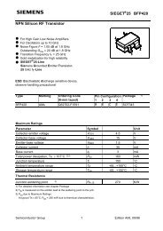
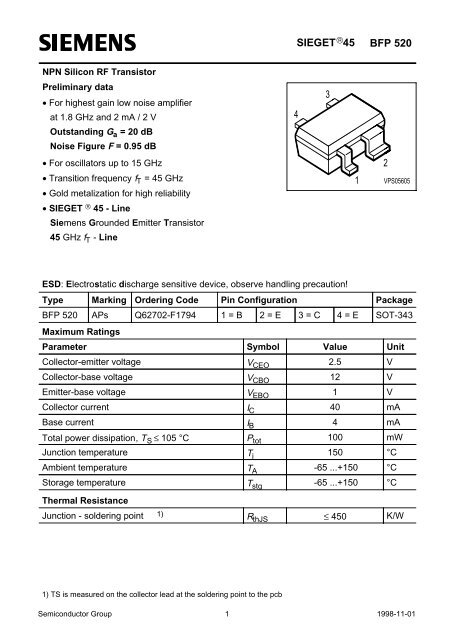
<strong>SIEGET</strong> ® <strong>45</strong><strong>BFP</strong> <strong>520</strong>NPN Silicon RF TransistorPreliminary data• For highest gain low noise amplifierat 1.8 GHz and 2 mA / 2 VOutstanding G a = 20 dBNoise Figure F = 0.95 dB• For oscillators up to 15 GHz• Transition frequency f T = <strong>45</strong> GHz• Gold metalization for high reliability• <strong>SIEGET</strong> ® <strong>45</strong> - LineSiemens Grounded Emitter Transistor<strong>45</strong> GHz f T - Line4312VPS05605ESD: Electrostatic discharge sensitive device, observe handling precaution!Type Marking Ordering Code Pin Configuration Package<strong>BFP</strong> <strong>520</strong> APs Q62702-F1794 1 = B 2 = E 3 = C 4 = E SOT-343Maximum RatingsParameter Symbol Value UnitCollector-emitter voltage V CEO 2.5 VCollector-base voltage V CBO 12 VEmitter-base voltage V EBO 1 VCollector current I C 40 mABase current I B 4 mATotal power dissipation, T S ≤ 105 °C P tot 100 mWJunction temperature T j 150 °CAmbient temperature T A -65 ...+150 °CStorage temperature T stg -65 ...+150 °CThermal ResistanceJunction - soldering point 1) R thJS ≤ <strong>45</strong>0 K/W1) TS is measured on the collector lead at the soldering point to the pcbSemiconductor GroupSemiconductor Group 1 1Sep-09-1998 1998-11-01
<strong>BFP</strong> <strong>520</strong>Electrical Characteristics at T A = 25°C, unless otherwise specified.Parameter Symbol Values Unitmin. typ. max.DC characteristicsCollector-emitter breakdown voltageV (BR)CEO2.5 3 3.5 VI C = 1 mA, I B = 0Collector-base cutoff currentI CBO- - 200 nAV CB = 5 V, I E = 0Emitter-base cutoff currentI EBO- - 35 nAV EB = 1.5 V, I C = 0DC current gainI C = 20 mA, V CE = 4 Vh FE50 80 150 -AC characteristicsTransition frequencyI C = 30 mA, V CE = 2 V, f = 2 GHzCollector-base capacitanceV CB = 2 V, f = 1 MHzCollector-emitter capacitanceV CE = 2 V, f = 1 MHzEmitter-base capacitanceV EB = 0.5 V, f = 1 MHzNoise figureI C = 2 mA, V CE = 2 V, Z S = Z Sopt ,f = 1.8 GHzPower gain 1)I C = 20 mA, V CE = 2 V, Z S = Z Sopt , Z L = Z Lopt ,f = 1.8 GHzInsertion power gainI C = 20 mA, V CE = 2 V, f = 1.8 GHz,Z S = Z L = 50ΩThird order intercept point at outputV CE = 2 V, f = 1.8 GHz, Z S =Z Sopt , Z L =Z Lopt ,I C = 20 mAI C = 7 mA1dB compression pointV CE = 2 V, f = 1.8 GHz, Z S =Z Sopt , Z L =Z Lopt ,I C = 20 mAI C = 7 mAf TC cb- <strong>45</strong>-0.06C ce- 0.3C eb- 0.35F -G ms|S 21 | 2IP 3P -1dB------0.9523212517125- GHz- pF- pF--pFdB- dB- dB----dBmdBm1) G ms = |S 21 / S 12 | 2) G ma = |S 21 / S 12 | (k-(k 2 -1) 1/2 )Semiconductor GroupSemiconductor Group 2 2Sep-09-1998 1998-11-01
<strong>BFP</strong> <strong>520</strong>Common Emitter S-Parametersf S 11 S 21 S 12 S 22GHz MAG ANG MAG ANG MAG ANG MAG ANGV CE = 2 V, / C = 20 mA0.010.10.5123<strong>45</strong>60.72440.72510.63680.47680.28160.2250.25<strong>520</strong>.32070.3675-0.7-8.4-40.7-73.6-123.8-166156.2133.6118.732.27331.63727.29319.611.027.485.6364.4883.683178.6171.4140.7113.584.967.65339.727.50.00070.00410.01940.03510.005740.07880.09940.11770.134369.492.875.966.556.349.241.532.924.70.90<strong>520</strong>.93630.85230.64960.38180.24070.15440.0950.05<strong>45</strong>1.2-4.4-26.7-46-64.6-73.6-95.3-128.9177.6Common Emitter Noise Parametersf F 1) min G 1) a Γ opt R N r n F 2) 50Ω |S 21 | 2 2)GHz dB dB MAG ANG Ω - dB dBV CE = 2 V, I C = 2 mA0.91.82.43<strong>45</strong>60.720.951.071.31.351.71.9521.<strong>520</strong>1614.511.69.580.640.490.<strong>45</strong>0.40.260.140.12143041548212815121.5191816.512.5980.430.380.360.330.250.180.161.751.551.61.71.61.851.9516.115.1414.0713.1311.499.878.28V CE = 2 V, I C = 5 mA0.91.82.43<strong>45</strong>60.891.081.121.321.351.61.82220.51816.213.511.510.50.490.380.340.290.1560.080.07122233<strong>45</strong>7112015016141413.5111080.320.280.280.270.220.20.161.51.381.41.51.<strong>45</strong>1.651.821.9419.3417.5416.0113.8211.9310.231) Input matched for minimum noise figure, output for maximum gain 2) Z S = Z L = 50ΩFor more and detailed S- and Noise-parameters please contact your local Siemensdistributor or sales office to obtain a Siemens Application Notes CD-ROM or see Internet:http://www.siemens.de/Semiconductor/products/35/35.htmSemiconductor GroupSemiconductor Group 3 3Sep-09-1998 1998-11-01
<strong>BFP</strong> <strong>520</strong>SPICE Parameters (Gummel-Poon Model, Berkley-SPICE 2G.6 Syntax) :Transistor Chip DataIS = tbd aAVAF = tbd VNE = tbd -VAR = tbd VNC = tbd -RBM = tbd ΩCJE = tbd fFTF = tbd psITF = tbd mAVJC = tbd VTR = tbd nsMJS = tbd -XTI = tbd -BF = tbd -IKF = tbd ABR = tbd -IKR = tbd ARB = tbd ΩRE = tbd ΩVJE = tbd VXTF = tbd -PTF = tbd degMJC = tbd -CJS = tbd fFXTB = tbd -FC = tbd -NF = tbd -ISE = tbd fANR = tbd -ISC = tbd fAIRB = tbd mARC = tbd ΩMJE = tbd -VTF = tbd VCJC = tbd fFXCJC = tbd -VJS = tbd VEG = tbd eVTNOM tbd KC’-E’-Diode Data (Berkley-SPICE 2G.6 Syntax) :IS = tbd fA N = tbd - RS = tbd ΩAll parameters are ready to use, no scalling is necessaryPackage Equivalent Circuit:C CBL BI = 0.47 nHL BO = 0.53 nHBL BOL BIB’TransistorChipE’C’L CIC’-E’-DiodeL COCL EI = 0.23 nHL EO = 0.05 nHL CI = 0.56 nHC BEC CEL CO = 0.58 nHL EIC BE = 136 fFC CB = 6.9 fFL EOC CE = 134 fFEEHA07389Valid up to 6GHzThe SOT-343 package has two emitter leads. To avoid high complexity of the package equivalent circuit,both leads are combined in one electrical connection.Extracted on behalf of SIEMENS Small Signal Semiconductors by:Institut für Mobil-und Satellitentechnik (IMST)© 1996 SIEMENS AGFor examples and ready to use parameters please contact your local Siemens distributor or sales office toobtain a Siemens CD-ROM or see Internet: http://www.siemens.de/Semiconductor/products/35/35.htmSemiconductor GroupSemiconductor Group 4 4Sep-09-1998 1998-11-01
<strong>BFP</strong> <strong>520</strong>For non-linear simulation:• Use transistor chip parameters in Berkeley SPICE 2G.6 syntax for all simulators.• If you need simulation of thereverse characteristics, add the diode with theC’-E’- diode data between collector and emitter.• Simulation of package is not necessary for frequenties < 100MHz.For higher frequencies add the wiring of package equivalent circuit around thenon-linear transistor and diode model.Note:• This transistor is constructed in a common emitter configuration. This feature causesan additional reverse biased diode between emitter and collector, which does noteffect normal operation.BCEEEHA07307Transistor Schematic DiagramThe common emitter configuration shows the following advantages:• Higher gain because of lower emitter inductance.• Power is dissipated via the grounded emitter leads, because the chip is mountedon copper emitter leadframe.Please note, that the broadest lead is the emitter lead.The AC characteristics are verified by random sampling.Semiconductor GroupSemiconductor Group 5 5Sep-09-1998 1998-11-01
<strong>BFP</strong> <strong>520</strong>Total power dissipation P tot = f (T A *, T S )* Package mounted on epoxyf = 2 GHzPtot120mW1009080706050403020Transition frequency f T = f (I C )V CE = parameter in V52GHz4440T S3632T AfT28242016128210.751040.500 20 40 60 80 100 120 °C 150T A ,T SPermissible Pulse Load R thJS = f (t p )00 5 10 15 20 25 30 35 mA <strong>45</strong>I CPermissible Pulse LoadP totmax /P totDC = f (t p )310110RthJSK/W0.50.20.10.050.020.010.005D = 0Pmax/ PDC-D = 00.0050.010.020.050.10.20.510210 -7 10 -6 10 -5 10 -4 10 -3 10 -2 s 10 0t p10010 -7 10 -6 10 -5 10 -4 10 -3 10 -2 s 10 0t pSemiconductor GroupSemiconductor Group 6 6Sep-09-1998 1998-11-01
<strong>BFP</strong> <strong>520</strong>Power gain G ma , G ms , |S 21 | 2 = f ( f )V CE = 2V, I C = 20 mA44dBPower gain G ma , G ms = f (I C )V CE = 2Vf = parameter in GHz32dB0.936G322824201612|S 21 |2G msG maG2420161281.82.43<strong>45</strong>684400.0 1.0 2.0 3.0 4.0 GHz 6.0f00 5 10 15 20 25 30 35 mA <strong>45</strong>I CPower gain G ma , G ms = f (V CE )I C = 20 mAf = parameter in GHz32Collector-base capacitance C cb = f (V CB )V BE = 0, f = 1MHz0.35dB0.9pF241.82.40.25G203Ccb0.2016412560.1580.1040.0500.0 0.5 1.0 1.5 2.0 V 3.0V CE0.000.0 0.5 1.0 1.5 2.0 V 3.0V CBSemiconductor GroupSemiconductor Group 7 7Sep-09-1998 1998-11-01
<strong>BFP</strong> <strong>520</strong>Noise figure F = f (I C )V CE = 2 V, Z S = Z SoptNoise figure F = f (I C )V CE = 2 V, f = 1.8 GHz3.03.0dBdB2.02.0FF1.51.51.00.5f = 6 GHzf = 5 GHzf = 4 GHzf = 3 GHzf = 2.4 GHzf = 1.8 GHzf = 0.9 GHz1.00.5Zs = 50OhmZs = Zsopt0.00 5 10 15 20 25 30 mA 40I C0.00 5 10 15 20 25 30 mA 40I CNoise figure F = f ( f )V CE = 2 V, Z S = Z Sopt3.0Source impedance for min.Noise Figuren vers. FrequencyV CE = 2 V, I C = 2 mA / 5 mA+j50dB+j25+j1002.0+j104GHz3GHz1.8GHzF5GHz0.9GHz1.50106GHz25501000.<strong>45</strong>GHz1.0-j102mA5mA0.5IC = 5 mAIC = 2 mA-j25-j100-j500.00.0 1.0 2.0 3.0 4.0 5.0 GHz 6.5fSemiconductor GroupSemiconductor Group 8 8Sep-09-1998 1998-11-01