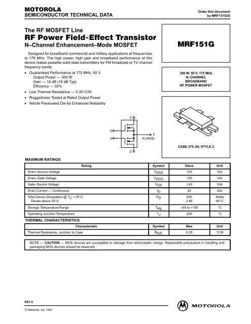
RF Power Field-Effect Transistor MRF151G - CB Tricks
RF Power Field-Effect Transistor MRF151G - CB Tricks
RF Power Field-Effect Transistor MRF151G - CB Tricks
- No tags were found...

Create successful ePaper yourself
Turn your PDF publications into a flip-book with our unique Google optimized e-Paper software.
TYPICAL CHARACTERISTICS10002000C, CAPACITANCE (pF)5002001005020CissCossCrssf T, UNITY GAIN FREQUENCY (MHz)1000VDS = 30 V15 V00 10 20 30 40 50VDS, DRAIN–SOURCE VOLTAGE (VOLTS)Figure 2. Capacitance versusDrain–Source Voltage**Data shown applies to each half of M<strong>RF</strong>151G.0 0 2 4 6 8 10 12 14 16 18 20ID, DRAIN CURRENT (AMPS)Figure 3. Common Source Unity Gain Frequencyversus Drain Current*VGS , DRAIN-SOURCE VOLTAGE (NORMALIZED)1.041.031.02ID = 5 A1.0114 A0.990.980.972 A0.960.951 A0.940.930.92250 mA0.910.9100 mA– 25 0 25 50 75 100ID, DRAIN CURRENT (AMPS)10010TC = 25°C1 2 20 200TC, CASE TEMPERATURE (°C)Figure 4. Gate–Source Voltage versusCase Temperature*VDS, DRAIN–TO–SOURCE VOLTAGE (VOLTS)Figure 5. DC Safe Operating AreaHIGH IMPEDANCEWINDINGSCENTERTAP9:1IMPEDANCERATIOCENTERTAP4:1IMPEDANCERATIOCONNECTIONSTO LOW IMPEDANCEWINDINGSFigure 6. <strong>RF</strong> TransformerMOTOROLA <strong>RF</strong> DEVICE DATAM<strong>RF</strong>151G3
TYPICAL CHARACTERISTICSPout, OUTPUT POWER (WATTS)35030025020015010050f = 150 MHzVDD = 50 VIDQ = 2 x 250 mA175 MHz200 MHzGPS, POWER GAIN (dB)3025201510VDD = 50 VIDQ = 2 x 250 mAPout = 150 W0 0 5 10Pin, INPUT POWER (WATTS)Figure 7. Output <strong>Power</strong> versus Input <strong>Power</strong>5 2 5 10 30 100 200f, FREQUENCY (MHz)Figure 8. <strong>Power</strong> Gain versus Frequency125150f = 175 MHz100INPUT, Zin(GATE TO GATE)Zo = 10 Ω3012510030150f = 175 MHzOUTPUT, ZOL*(DRAIN TO DRAIN)ZOL* = Conjugate of the optimum load impedanceZOL* = into which the device output operates at aZOL* = given output power, voltage and frequency.Figure 9. Input and Output ImpedanceM<strong>RF</strong>151G4MOTOROLA <strong>RF</strong> DEVICE DATA
<strong>RF</strong> POWER MOSFET CONSIDERATIONSMOSFET CAPACITANCESThe physical structure of a MOSFET results in capacitorsbetween the terminals. The metal anode gate structure determinesthe capacitors from gate–to–drain (Cgd), and gate–to–source (Cgs). The PN junction formed during thefabrication of the <strong>RF</strong> MOSFET results in a junction capacitancefrom drain–to–source (Cds).These capacitances are characterized as input (Ciss), output(Coss) and reverse transfer (Crss) capacitances on datasheets. The relationships between the inter–terminal capacitancesand those given on data sheets are shown below. TheCiss can be specified in two ways:1. Drain shorted to source and positive voltage at the gate.2. Positive voltage of the drain in respect to source and zerovolts at the gate. In the latter case the numbers are lower.However, neither method represents the actual operatingconditions in <strong>RF</strong> applications.GATECgdCgsDRAINCdsSOURCECiss = Cgd = CgsCoss = Cgd = CdsCrss = CgdLINEARITY AND GAIN CHARACTERISTICSIn addition to the typical IMD and power gain data presented,Figure 3 may give the designer additional informationon the capabilities of this device. The graph represents thesmall signal unity current gain frequency at a given drain currentlevel. This is equivalent to fT for bipolar transistors.Since this test is performed at a fast sweep speed, heating ofthe device does not occur. Thus, in normal use, the highertemperatures may degrade these characteristics to some extent.DRAIN CHARACTERISTICSOne figure of merit for a FET is its static resistance in thefull–on condition. This on–resistance, VDS(on), occurs in thelinear region of the output characteristic and is specified underspecific test conditions for gate–source voltage and draincurrent. For MOSFETs, VDS(on) has a positive temperaturecoefficient and constitutes an important design considerationat high temperatures, because it contributes to the powerdissipation within the device.GATE CHARACTERISTICSThe gate of the MOSFET is a polysilicon material, and iselectrically isolated from the source by a layer of oxide. Theinput resistance is very high — on the order of 109 ohms —resulting in a leakage current of a few nanoamperes.Gate control is achieved by applying a positive voltageslightly in excess of the gate–to–source threshold voltage,VGS(th).Gate Voltage Rating — Never exceed the gate voltagerating. Exceeding the rated VGS can result in permanentdamage to the oxide layer in the gate region.Gate Termination — The gates of these devices are essentiallycapacitors. Circuits that leave the gate open–circuitedor floating should be avoided. These conditions canresult in turn–on of the devices due to voltage build–up onthe input capacitor due to leakage currents or pickup.Gate Protection — These devices do not have an internalmonolithic zener diode from gate–to–source. If gate protectionis required, an external zener diode is recommended.Using a resistor to keep the gate–to–source impedancelow also helps damp transients and serves another importantfunction. Voltage transients on the drain can be coupled tothe gate through the parasitic gate–drain capacitance. If thegate–to–source impedance and the rate of voltage changeon the drain are both high, then the signal coupled to the gatemay be large enough to exceed the gate–threshold voltageand turn the device on.HANDLING CONSIDERATIONSWhen shipping, the devices should be transported only inantistatic bags or conductive foam. Upon removal from thepackaging, careful handling procedures should be adheredto. Those handling the devices should wear grounding strapsand devices not in the antistatic packaging should be kept inmetal tote bins. MOSFETs should be handled by the caseand not by the leads, and when testing the device, all leadsshould make good electrical contact before voltage is applied.As a final note, when placing the FET into the system itis designed for, soldering should be done with a groundediron.DESIGN CONSIDERATIONSThe M<strong>RF</strong>151G is an <strong>RF</strong> <strong>Power</strong>, MOS, N–channel enhancementmode field–effect transistor (FET) designed forHF and VHF power amplifier applications.Motorola Application Note AN211A, FETs in Theory andPractice, is suggested reading for those not familiar with theconstruction and characteristics of FETs.The major advantages of <strong>RF</strong> power MOSFETs includehigh gain, low noise, simple bias systems, relative immunityfrom thermal runaway, and the ability to withstand severelymismatched loads without suffering damage. <strong>Power</strong> outputcan be varied over a wide range with a low power dc controlsignal.DC BIASThe M<strong>RF</strong>151G is an enhancement mode FET and, therefore,does not conduct when drain voltage is applied. Draincurrent flows when a positive voltage is applied to the gate.<strong>RF</strong> power FETs require forward bias for optimum performance.The value of quiescent drain current (IDQ) is not criticalfor many applications. The M<strong>RF</strong>151G was characterizedat IDQ = 250 mA, each side, which is the suggested minimumvalue of IDQ. For special applications such as linear amplification,IDQ may have to be selected to optimize the criticalparameters.The gate is a dc open circuit and draws no current. Therefore,the gate bias circuit may be just a simple resistive dividernetwork. Some applications may require a more elaboratebias sytem.GAIN CONTROL<strong>Power</strong> output of the M<strong>RF</strong>151G may be controlled from itsrated value down to zero (negative gain) by varying the dcgate voltage. This feature facilitates the design of manualgain control, AGC/ALC and modulation systems.MOTOROLA <strong>RF</strong> DEVICE DATAM<strong>RF</strong>151G5
PACKAGE DIMENSIONSREK1 23 4DUGN5Q RADIUS 2 PL0.25 (0.010) M T A M B M–B–JNOTES:1. DIMENSIONING AND TOLERANCING PER ANSIY14.5M, 1982.2. CONTROLLING DIMENSION: INCH.INCHES MILLIMETERSDIM MIN MAX MIN MAXA 1.330 1.350 33.79 34.29B 0.370 0.410 9.40 10.41C 0.190 0.230 4.83 5.84D 0.215 0.235 5.47 5.96E 0.050 0.070 1.27 1.77G 0.430 0.440 10.92 11.18H 0.102 0.112 2.59 2.84J 0.004 0.006 0.11 0.15K 0.185 0.215 4.83 5.33N 0.845 0.875 21.46 22.23Q 0.060 0.070 1.52 1.78R 0.390 0.410 9.91 10.41U 1.100 BSC 27.94 BSCH–A–C–T–SEATINGPLANESTYLE 2:PIN 1. DRAIN2. DRAIN3. GATE4. GATE5. SOURCECASE 375–04ISSUE DMotorola reserves the right to make changes without further notice to any products herein. Motorola makes no warranty, representation or guarantee regardingthe suitability of its products for any particular purpose, nor does Motorola assume any liability arising out of the application or use of any product or circuit,and specifically disclaims any and all liability, including without limitation consequential or incidental damages. “Typical” parameters can and do vary in differentapplications. All operating parameters, including “Typicals” must be validated for each customer application by customer’s technical experts. Motorola doesnot convey any license under its patent rights nor the rights of others. Motorola products are not designed, intended, or authorized for use as components insystems intended for surgical implant into the body, or other applications intended to support or sustain life, or for any other application in which the failure ofthe Motorola product could create a situation where personal injury or death may occur. Should Buyer purchase or use Motorola products for any suchunintended or unauthorized application, Buyer shall indemnify and hold Motorola and its officers, employees, subsidiaries, affiliates, and distributors harmlessagainst all claims, costs, damages, and expenses, and reasonable attorney fees arising out of, directly or indirectly, any claim of personal injury or deathassociated with such unintended or unauthorized use, even if such claim alleges that Motorola was negligent regarding the design or manufacture of the part.Motorola and are registered trademarks of Motorola, Inc. Motorola, Inc. is an Equal Opportunity/Affirmative Action Employer.How to reach us:USA / EUROPE: Motorola Literature Distribution;JAPAN: Nippon Motorola Ltd.; Tatsumi–SPD–JLDC, Toshikatsu Otsuki,P.O. Box 20912; Phoenix, Arizona 85036. 1–800–441–2447 6F Seibu–Butsuryu–Center, 3–14–2 Tatsumi Koto–Ku, Tokyo 135, Japan. 03–3521–8315MFAX: RMFAX0@email.sps.mot.com – TOUCHTONE (602) 244–6609 HONG KONG: Motorola Semiconductors H.K. Ltd.; 8B Tai Ping Industrial Park,INTERNET: http://Design–NET.com 51 Ting Kok Road, Tai Po, N.T., Hong Kong. 852–26629298M<strong>RF</strong>151G6◊MOTOROLA <strong>RF</strong> DEVICE M<strong>RF</strong>151G/D DATA