16K I2C Serial EEPROM - Hifi-remote.com
16K I2C Serial EEPROM - Hifi-remote.com
16K I2C Serial EEPROM - Hifi-remote.com
- No tags were found...

Create successful ePaper yourself
Turn your PDF publications into a flip-book with our unique Google optimized e-Paper software.
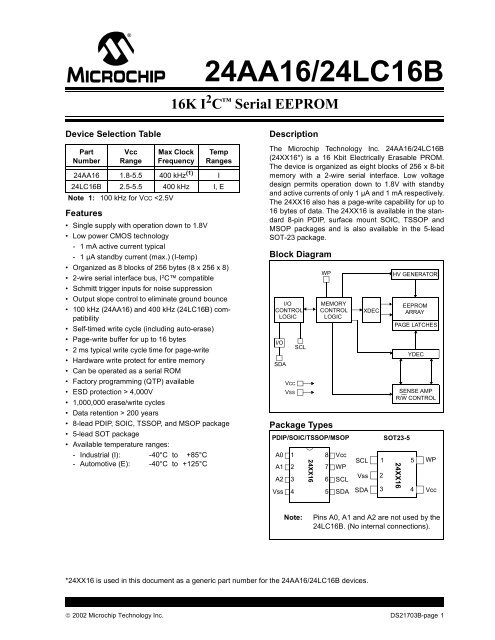
M24AA16/24LC16B<strong>16K</strong> I 2 C <strong>Serial</strong> <strong>EEPROM</strong>Device Selection TablePartNumberFeaturesVccRangeMax ClockFrequencyTempRanges24AA16 1.8-5.5 400 kHz (1) I24LC16B 2.5-5.5 400 kHz I, ENote 1: 100 kHz for VCC 4,000V• 1,000,000 erase/write cycles• Data retention > 200 years• 8-lead PDIP, SOIC, TSSOP, and MSOP package• 5-lead SOT package• Available temperature ranges:- Industrial (I): -40°C to +85°C- Automotive (E): -40°C to +125°CDescriptionThe Microchip Technology Inc. 24AA16/24LC16B(24XX16*) is a 16 Kbit Electrically Erasable PROM.The device is organized as eight blocks of 256 x 8-bitmemory with a 2-wire serial interface. Low voltagedesign permits operation down to 1.8V with standbyand active currents of only 1 µA and 1 mA respectively.The 24XX16 also has a page-write capability for up to16 bytes of data. The 24XX16 is available in the standard8-pin PDIP, surface mount SOIC, TSSOP andMSOP packages and is also available in the 5-leadSOT-23 package.Block DiagramI/OCONTROLLOGICI/OSDAVCCVSSSCLWPPackage TypesA0A1A2Vss123424XX16MEMORYCONTROLLOGICPDIP/SOIC/TSSOP/MSOP8765VccWPSCLSDASCLVssSDAXDECHV GENERATOR<strong>EEPROM</strong>ARRAYPAGE LATCHESYDECSENSE AMPR/W CONTROLSOT23-51 52324XX164WPVccNote:Pins A0, A1 and A2 are not used by the24LC16B. (No internal connections).*24XX16 is used in this document as a generic part number for the 24AA16/24LC16B devices.© 2002 Microchip Technology Inc. DS21703B-page 1
24AA16/24LC16B1.0 ELECTRICAL CHARACTERISTICSAbsolute Maximum Ratings†VCC.............................................................................................................................................................................6.5VAll inputs and outputs w.r.t. VSS ......................................................................................................... -0.3V to VCC +1.0VStorage temperature ...............................................................................................................................-65°C to +150°CAmbient temp. with power applied ..........................................................................................................-40°C to +125°CESD protection on all pins ......................................................................................................................................................≥ 4kV† NOTICE: Stresses above those listed under “Maximum ratings” may cause permanent damage to the device.This is a stress rating only and functional operation of the device at those or any other conditions above thoseindicated in the operational listings of this specification is not implied. Exposure to maximum rating conditionsfor extended periods may affect device reliability.1.1 DC CharacteristicsDC CHARACTERISTICSParam.No.VCC = +1.8V to +5.5VIndustrial (I): TAMB = -40°C to +85°CAutomotive (E): TAMB = -40°C to +125°CSym Characteristic Min Typ Max Units ConditionsD1 VIH WP, SCL and SDA pins — — — — —D2 — High level input voltage 0.7 VCC — — V —D3 VIL Low level input voltage — — 0.3 VCC V —D4 VHYS Hysteresis of Schmitt .05 VCC — — V (Note 1)trigger inputsD5 VOL Low level output voltage — — 0.40 V IOL = 3.0 mA, VCC = 2.5VD6 ILI Input leakage current — — ±10 µA VIN =.1V to VCCD7 ILO Output leakage current — — ±10 µA VOUT =.1V to VCCD8 CIN,COUTPin capacitance(all inputs/outputs)— — 10 pF VCC = 5.0V (Note 1)TAMB = 25°C, FCLK = 1 MHzD9 ICC write Operating current — — 3 mA VCC = 5.5V, SCL = 400 kHzD10 ICC read — 0.01 1 mA —D11 ICCS Standby current ——0.3.01Note 1: This parameter is periodically sampled and not 100% tested.2: Typical measurements taken at room temperature.15µΑµΑIndustrialAutomotiveSDA = SCL = VCCWP = VSSDS21703B-page 2© 2002 Microchip Technology Inc.
24AA16/24LC16B1.2 AC CharacteristicsAC CHARACTERISTICSParam.No.VCC = +1.8V to +5.5VIndustrial (I): TAMB = -40°C to +85°CAutomotive (E): TAMB = -40°C to +125°CSym Characteristic Min Max Units Conditions1 FCLK Clock frequency ——2 THIGH Clock high time 60040003 TLOW Clock low time 130047004 TR SDA and SCL rise time(Note 1)——400100————30010005 TF SDA and SCL fall time — 300 ns (Note 1)6 THD:STA START condition hold time 60040007 TSU:STA START condition setup time 60047008 THD:DAT Data input hold time 0 — ns (Note 2)9 TSU:DAT Data input setup time 10025010 TSU:STO STOP condition setup time 600400011 TAA Output valid from clock(Note 2)12 TBUF Bus free time: Time the busmust be free before a newtransmission can start13 TOF Output fall time from VIH minimumto VIL maximum14 TSP Input filter spike suppression(SDA and SCL pins)15 TWC Write cycle time (byte orpage)——1300470020+0.1CB—————————9003500——250250kHz 2.5V ≤ VCC ≤ 5.5V1.8V ≤ VCC < 2.5V (24AA16)ns 2.5V ≤ VCC ≤ 5.5V1.8V ≤ VCC < 2.5V (24AA16)ns 2.5V ≤ VCC ≤ 5.5V1.8V ≤ VCC < 2.5V (24AA16)ns 2.5V ≤ VCC ≤ 5.5V (Note 1)1.8V ≤ VCC < 2.5V (24AA16)(Note 1)ns 2.5V ≤ VCC ≤ 5.5V1.8V ≤ VCC < 2.5V (24AA16)ns 2.5V ≤ VCC ≤ 5.5V1.8V ≤ VCC < 2.5V (24AA16)ns 2.5V ≤ VCC ≤ 5.5V1.8V ≤ VCC < 2.5V (24AA16)ns 2.5V ≤ VCC ≤ 5.5V1.8V ≤ VCC < 2.5V (24AA16)ns 2.5V ≤ VCC ≤ 5.5V1.8V ≤ VCC < 2.5V (24AA16)ns 2.5V ≤ VCC ≤ 5.5V1.8V ≤ VCC < 2.5V (24AA16)ns 2.5V ≤ VCC ≤ 5.5V1.8V ≤ VCC ≤ 2.5V (24AA16)— 50 ns (Notes 1 and 3)— 5 ms —16 — Endurance 1M — cycles 25°C, VCC = 5.0V, Block Mode(Note 4)Note 1: Not 100% tested. CB = total capacitance of one bus line in pF.2: As a transmitter, the device must provide an internal minimum delay time to bridge the undefined region(minimum 300 ns) of the falling edge of SCL to avoid unintended generation of START or STOP conditions.3: The <strong>com</strong>bined TSP and VHYS specifications are due to new Schmitt trigger inputs which provide improvednoise spike suppression. This eliminates the need for a TI specification for standard operation.4: This parameter is not tested but ensured by characterization. For endurance estimates in a specific application,please consult the Total Endurance Model which can be obtained on Microchip’s website:www.microchip.<strong>com</strong>.© 2002 Microchip Technology Inc. DS21703B-page 3
24AA16/24LC16BFIGURE 1-1:BUS TIMING DATA5324SCLSDAIN14768 9 101112SDAOUTFIGURE 1-2:BUS TIMING START/STOPD4SCL7610SDASTARTSTOPDS21703B-page 4© 2002 Microchip Technology Inc.
24AA16/24LC16B2.0 FUNCTIONAL DESCRIPTIONThe 24XX16 supports a bi-directional 2-wire bus anddata transmission protocol. A device that sends dataonto the bus is defined as transmitter, and a devicereceiving data as receiver. The bus has to be controlledby a master device which generates the serial clock(SCL), controls the bus access and generates theSTART and STOP conditions, while the 24XX16 worksas slave. Both master and slave can operate as transmitteror receiver, but the master device determineswhich mode is activated.3.0 BUS CHARACTERISTICSThe following bus protocol has been defined:• Data transfer may be initiated only when the busis not busy.• During data transfer, the data line must remainstable whenever the clock line is HIGH. Changesin the data line while the clock line is HIGH will beinterpreted as a START or STOP condition.Accordingly, the following bus conditions have beendefined (Figure 3-1).3.1 Bus not Busy (A)Both data and clock lines remain HIGH.3.2 Start Data Transfer (B)A HIGH to LOW transition of the SDA line while theclock (SCL) is HIGH determines a START condition. All<strong>com</strong>mands must be preceded by a START condition.3.3 Stop Data Transfer (C)A LOW to HIGH transition of the SDA line while theclock (SCL) is HIGH determines a STOP condition. Alloperations must be ended with a STOP condition.3.4 Data Valid (D)The state of the data line represents valid data when,after a START condition, the data line is stable for theduration of the HIGH period of the clock signal.The data on the line must be changed during the LOWperiod of the clock signal. There is one clock pulse perbit of data.Each data transfer is initiated with a START conditionand terminated with a STOP condition. The number ofthe data bytes transferred between the START andSTOP conditions is determined by the master deviceand is theoretically unlimited, although only the last sixteenwill be stored when doing a write operation. Whenan overwrite does occur it will replace data in a first-infirst-out (FIFO) fashion.3.5 AcknowledgeEach receiving device, when addressed, is obliged togenerate an acknowledge after the reception of eachbyte. The master device must generate an extra clockpulse which is associated with this acknowledge bit.Note:The 24XX16 does not generate anyacknowledge bits if an internal programmingcycle is in progress.The device that acknowledges, has to pull down theSDA line during the acknowledge clock pulse in such away that the SDA line is stable LOW during the HIGHperiod of the acknowledge related clock pulse. Ofcourse, setup and hold times must be taken intoaccount. During reads, a master must signal an end ofdata to the slave by not generating an acknowledge biton the last byte that has been clocked out of the slave.In this case, the slave (24XX16) will leave the data lineHIGH to enable the master to generate the STOP condition.FIGURE 3-1:DATA TRANSFER SEQUENCE ON THE SERIAL BUSSCL(A) (B) (D) (D) (C) (A)SDASTARTCONDITIONADDRESS ORACKNOWLEDGEVALIDDATAALLOWEDTO CHANGESTOPCONDITION© 2002 Microchip Technology Inc. DS21703B-page 5
24AA16/24LC16B3.6 Device AddressingA control byte is the first byte received following thestart condition from the master device. The control byteconsists of a four bit control code, for the 24XX16 thisis set as 1010 binary for read and write operations.The next three bits of the control byte are the blockselect bits (B2, B1, B0). They are used by the masterdevice to select which of the eight 256 word blocks ofmemory are to be accessed. These bits are in effect thethree most significant bits of the word address. Itshould be noted that the protocol limits the size of thememory to eight blocks of 256 words, therefore the protocolcan support only one 24XX16 per system.The last bit of the control byte defines the operation tobe performed. When set to ‘1’ a read operation isselected, when set to ‘0’ a write operation is selected.Following the START condition, the 24XX16 monitorsthe SDA bus checking the device type identifier beingtransmitted, upon a 1010 code the slave device outputsan acknowledge signal on the SDA line. Dependingon the state of the R/W bit, the 24XX16 will select aread or write operation.OperationControlCodeBlock SelectR/WRead 1010 Block Address 1Write 1010 Block Address 0FIGURE 3-2:STARTCONTROL BYTEALLOCATIONSLAVE ADDRESSREAD/WRITER/W1 0 1 0 B2 B1 B0ADS21703B-page 6© 2002 Microchip Technology Inc.
24AA16/24LC16B4.0 WRITE OPERATION4.1 Byte WriteFollowing the START condition from the master, thedevice code (4 bits), the block address (3 bits) and theR/W bit which is a logic LOW is placed onto the bus bythe master transmitter. This indicates to the addressedslave receiver that a byte with a word address will followafter it has generated an acknowledge bit duringthe ninth clock cycle. Therefore, the next byte transmittedby the master is the word address and will be writteninto the address pointer of the 24XX16. Afterreceiving another acknowledge signal from the24XX16, the master device will transmit the data wordto be written into the addressed memory location. The24XX16 acknowledges again and the master generatesa STOP condition. This initiates the internal writecycle, and during this time the 24XX16 will not generateacknowledge signals (Figure 4-1).4.2 Page WriteThe write control byte, word address and the first databyte are transmitted to the 24XX16 in the same way asin a byte write. But instead of generating a STOP conditionthe master transmits up to 16 data bytes to the24XX16, which are temporarily stored in the on-chippage buffer and will be written into the memory after themaster has transmitted a STOP condition. After thereceipt of each word, the four lower order addresspointer bits are internally incremented by ‘1’. Thehigher order 7 bits of the word address remains constant.If the master should transmit more than 16 wordsprior to generating the STOP condition, the addresscounter will roll over and the previously received datawill be overwritten. As with the byte write operation,once the STOP condition is received an internal writecycle will begin (Figure 4-2).Note:Page write operations are limited to writingbytes within a single physical page,regardless of the number of bytes actuallybeing written. Physical page boundariesstart at addresses that are integermultiples of the page buffer size (or‘page size’) and end at addresses thatare integer multiples of [page size - 1]. Ifa page write <strong>com</strong>mand attempts to writeacross a physical page boundary, theresult is that the data wraps around tothe beginning of the current page (overwritingdata previously stored there),instead of being written to the next pageas might be expected. It is thereforenecessary for the application software toprevent page write operations thatwould attempt to cross a page boundary.FIGURE 4-1:BYTE WRITEBUS ACTIVITYMASTERSTARTCONTROLBYTEWORDADDRESSDATASTOPSDA LINESPBUS ACTIVITYACKACKACKFIGURE 4-2:PAGE WRITEBUS ACTIVITYMASTERSTARTCONTROLBYTEWORDADDRESS (n) DATA (n) DATA (n + 1) DATA (n + 15)STOPSDA LINEBUS ACTIVITYSACKACKACKACKACKP© 2002 Microchip Technology Inc. DS21703B-page 7
24AA16/24LC16B5.0 ACKNOWLEDGE POLLINGSince the device will not acknowledge during a writecycle, this can be used to determine when the cycle is<strong>com</strong>plete (this feature can be used to maximize busthroughput). Once the STOP condition for a write <strong>com</strong>mandhas been issued from the master, the device initiatesthe internally timed write cycle. ACK polling canbe initiated immediately. This involves the master sendinga start condition followed by the control byte for awrite <strong>com</strong>mand (R/W = 0). If the device is still busy withthe write cycle, then no ACK will be returned. If thecycle is <strong>com</strong>plete, then the device will return the ACKand the master can then proceed with the next read orwrite <strong>com</strong>mand. See Figure 5-1 for flow diagram.6.0 WRITE PROTECTIONThe 24XX16 can be used as a serial ROM when theWP pin is connected to VCC. Programming will beinhibited and the entire memory will be write-protected.FIGURE 5-1:ACKNOWLEDGE POLLINGFLOWSendWrite CommandSend StopCondition toInitiate Write CycleSend StartSend Control Bytewith R/W = 0Did DeviceAcknowledge(ACK = 0)?NoYesNextOperationDS21703B-page 8© 2002 Microchip Technology Inc.
24AA16/24LC16B7.0 READ OPERATIONRead operations are initiated in the same way as writeoperations with the exception that the R/W bit of theslave address is set to ‘1’. There are three basic typesof read operations: current address read, random readand sequential read.7.1 Current Address ReadThe 24XX16 contains an address counter that maintainsthe address of the last word accessed, internallyincremented by ‘1’. Therefore, if the previous access(either a read or write operation) was to address n, thenext current address read operation would access datafrom address n + 1. Upon receipt of the slave addresswith R/W bit set to ‘1’, the 24XX16 issues an acknowledgeand transmits the 8-bit data word. The master willnot acknowledge the transfer but does generate aSTOP condition and the 24XX16 discontinues transmission(Figure 7-1).7.2 Random ReadRandom read operations allow the master to accessany memory location in a random manner. To performthis type of read operation, first the word address mustbe set. This is done by sending the word address to the24XX16 as part of a write operation. After the wordaddress is sent, the master generates a START conditionfollowing the acknowledge. This terminates thewrite operation, but not before the internal addresspointer is set. Then the master issues the control byteagain but with the R/W bit set to a ‘1’. The 24XX16 willthen issue an acknowledge and transmits the 8-bit dataword. The master will not acknowledge the transfer butdoes generate a STOP condition and the 24XX16 discontinuestransmission (Figure 7-2).7.3 Sequential ReadSequential reads are initiated in the same way as a randomread except that after the 24XX16 transmits thefirst data byte, the master issues an acknowledge asopposed to a STOP condition in a random read. Thisdirects the 24XX16 to transmit the next sequentiallyaddressed 8-bit word (Figure 7-3).To provide sequential reads the 24XX16 contains aninternal address pointer which is incremented by one atthe <strong>com</strong>pletion of each operation. This address pointerallows the entire memory contents to be serially readduring one operation.7.4 Noise ProtectionThe 24XX16 employs a VCC threshold detector circuitwhich disables the internal erase/write logic if the VCCis below 1.5V at nominal conditions.The SCL and SDA inputs have Schmitt trigger and filtercircuits which suppress noise spikes to assure properdevice operation even on a noisy bus.FIGURE 7-1:CURRENT ADDRESS READBUS ACTIVITYMASTERSTARTCONTROLBYTEDATA (n)STOPSDA LINESPBUS ACTIVITYACKNOACK© 2002 Microchip Technology Inc. DS21703B-page 9
24AA16/24LC16BFIGURE 7-2:RANDOM READBUS ACTIVITYMASTERSTARTCONTROLBYTEWORDADDRESS (n)STARTCONTROLBYTEDATA (n)STOPSDA LINEBUS ACTIVITYSACKACKSACKNOACKPFIGURE 7-3:SEQUENTIAL READBUS ACTIVITYMASTERCONTROLBYTEDATA (n) DATA (n + 1) DATA (n + 2) DATA (n + X)STOPSDA LINEPBUS ACTIVITYACKACKACKACKNOACKDS21703B-page 10© 2002 Microchip Technology Inc.
24AA16/24LC16B8.0 PIN DESCRIPTIONSThe descriptions of the pins are listed in Table 8-1.TABLE 8-1:PIN FUNCTION TABLEName PDIP SOIC TSSOP MSOP SOT23 DescriptionA0 1 1 1 1 — Not ConnectedA1 2 2 2 2 — Not ConnectedA2 3 3 3 3 — Not ConnectedVSS 4 4 4 4 2 GroundSDA 5 5 5 5 3 <strong>Serial</strong> Address/Data I/OSCL 6 6 6 6 1 <strong>Serial</strong> ClockWP 7 7 7 7 5 Write Protect InputVCC 8 8 8 8 4 +1.8V to 5.5V Power Supply8.1 <strong>Serial</strong> Address/Data Input/Output(SDA)This is a bi-directional pin used to transfer addressesand data into and data out of the device. It is an opendrain terminal. Therefore, the SDA bus requires a pullupresistor to VCC (typical 10 kΩ for 100 kHz, 2 kΩ for400 kHz).For normal data transfer SDA is allowed to change onlyduring SCL LOW. Changes during SCL HIGH arereserved for indicating the START and STOP conditions.8.2 <strong>Serial</strong> Clock (SCL)This input is used to synchronize the data transfer fromand to the device.8.3 Write-Protect (WP)This pin must be connected to either VSS or VCC.If tied to VSS normal memory operation is enabled(read/write the entire memory 000-7FF).If tied to VCC, WRITE operations are inhibited. Theentire memory will be write-protected. Read operationsare not affected.This feature allows the user to use the 24XX16 as aserial ROM when WP is enabled (tied to VCC).8.4 A0, A1, A2These pins are not used by the 24XX16. They may beleft floating or tied to either VSS or VCC.© 2002 Microchip Technology Inc. DS21703B-page 11
24AA16/24LC16B9.0 PACKAGING INFORMATION9.1 Package Marking Information8-Lead PDIP (300 mil)XXXXXXXXXXXXXNNNYYWWExample:24LC16BI/PNNNYYWW8-Lead SOIC (150 mil)Example:XXXXXXXXXXXXYYWWNNN24LC16BI/SNYYWWNNN8-Lead TSSOPExample:XXXXXYWWNNN4L16IYWWNNN8-Lead MSOPXXXXXXYWWNNNExample:4L16BIYWWNNN5-Lead SOT-23Example:XXNN24AA16-I/OT = B524LC16B-I/OT = M5B5NNLegend: XX...X Customer specific information*YY Year code (last 2 digits of calendar year)WW Week code (week of January 1 is week ‘01’)NNN Alphanumeric traceability codeNote:In the event the full Microchip part number cannot be marked on one line, it willbe carried over to the next line thus limiting the number of available charactersfor customer specific information.* Standard OTP marking consists of Microchip part number, year code, week code, and traceability code.DS21703B-page 12© 2002 Microchip Technology Inc.
24AA16/24LC16B8-Lead Plastic Dual In-line (P) – 300 mil (PDIP)E12Dn1αEAA2cA1LβeBB1BpUnits INCHES* MILLIMETERSDimension Limits MIN NOM MAX MIN NOM MAXNumber of Pins n 8 8Pitch p .100 2.54Top to Seating Plane A .140 .155 .170 3.56 3.94 4.32Molded Package Thickness A2 .115 .130 .145 2.92 3.30 3.68Base to Seating Plane A1 .015 0.38Shoulder to Shoulder Width E .300 .313 .325 7.62 7.94 8.26Molded Package Width E1 .240 .250 .260 6.10 6.35 6.60Overall Length D .360 .373 .385 9.14 9.46 9.78Tip to Seating Plane L .125 .130 .135 3.18 3.30 3.43Lead Thickness c .008 .012 .015 0.20 0.29 0.38Upper Lead Width B1 .045 .058 .070 1.14 1.46 1.78Lower Lead Width B .014 .018 .022 0.36 0.46 0.56Overall Row Spacing § eB .310 .370 .430 7.87 9.40 10.92Mold Draft Angle Top α 5 10 15 5 10 15Mold Draft Angle Bottom β 5 10 15 5 10 15* Controlling Parameter§ Significant CharacteristicNotes:Dimensions D and E1 do not include mold flash or protrusions. Mold flash or protrusions shall not exceed.010” (0.254mm) per side.JEDEC Equivalent: MS-001Drawing No. C04-018© 2002 Microchip Technology Inc. DS21703B-page 13
24AA16/24LC16B8-Lead Plastic Small Outline (SN) – Narrow, 150 mil (SOIC)EE1p2DBn145×hαcAA2fβLA1UnitsINCHES*MILLIMETERSDimension Limits MIN NOM MAX MIN NOM MAXNumber of Pinsn88Pitchp.0501.27Overall HeightA .053 .061 .069 1.35 1.55 1.75Molded Package Thickness A2 .052 .056 .061 1.32 1.42 1.55Standoff §A1 .004 .007 .010 0.10 0.18 0.25Overall WidthE .228 .237 .244 5.79 6.02 6.20Molded Package WidthE1 .146 .154 .157 3.71 3.91 3.99Overall LengthD .189 .193 .197 4.80 4.90 5.00Chamfer Distanceh .010 .015 .020 0.25 0.38 0.51Foot LengthL .019 .025 .030 0.48 0.62 0.76Foot Angle f 0 4 8 0 4 8Lead Thicknessc .008 .009 .010 0.20 0.23 0.25Lead WidthB .013 .017 .020 0.33 0.42 0.51Mold Draft Angle Topα0 12 150 12 15Mold Draft Angle Bottomβ0 12 150 12 15* Controlling Parameter§ Significant CharacteristicNotes:Dimensions D and E1 do not include mold flash or protrusions. Mold flash or protrusions shall not exceed.010” (0.254mm) per side.JEDEC Equivalent: MS-012Drawing No. C04-057DS21703B-page 14© 2002 Microchip Technology Inc.
24AA16/24LC16B8-Lead Plastic Thin Shrink Small Outline (ST) – 4.4 mm (TSSOP)EE1p2DBn1AαcfA1A2βLUnitsINCHESMILLIMETERS*Dimension Limits MIN NOM MAX MIN NOM MAXNumber of Pinsn88Pitchp.0260.65Overall HeightA.0431.10Molded Package Thickness A2 .033 .035 .037 0.85 0.90 0.95Standoff §A1 .002 .004 .006 0.05 0.10 0.15Overall WidthE .246 .251 .256 6.25 6.38 6.50Molded Package WidthE1 .169 .173 .177 4.30 4.40 4.50Molded Package LengthD .114 .118 .122 2.90 3.00 3.10Foot LengthL .020 .024 .028 0.50 0.60 0.70Foot Angle f 0 4 8 0 4 8Lead Thicknessc .004 .006 .008 0.09 0.15 0.20Lead WidthB .007 .010 .012 0.19 0.25 0.30Mold Draft Angle Topα05 1005 10Mold Draft Angle Bottomβ05 1005 10* Controlling Parameter§ Significant CharacteristicNotes:Dimensions D and E1 do not include mold flash or protrusions. Mold flash or protrusions shall not exceed.005” (0.127mm) per side.JEDEC Equivalent: MO-153Drawing No. C04-086© 2002 Microchip Technology Inc. DS21703B-page 15
24AA16/24LC16B8-Lead Plastic Micro Small Outline Package (MSOP)EE1Bn 12Dαcφ(F)LβUnitsDimension LimitsNumber of PinsPitchOverall HeightMolded Package ThicknessnpAA2Standoff §A1Overall WidthEMolded Package WidthOverall LengthFoot LengthE1DLFootprint (Reference)Foot AngleLead ThicknessLead WidthMold Draft Angle TopMold Draft Angle Bottom*Controlling Parameter§ Significant CharacteristicNotes:FφcBαβINCHESMILLIMETERS*MIN NOM MAX MIN NOM MAX88.0260.65.0441.18.030.002.034 .038.0060.760.050.86 0.970.15.184 .193 .200 4.67 4.90 .5.08.114.114.016.118.118.022.122.122.0282.902.900.403.003.000.553.103.100.70.0350.004.010Dimensions D and E1 do not include mold flash or protrusions. Mold flash or protrusions shall notexceed .010" (0.254mm) per side..037.006.01277.0396.008.0160.9000.100.250.950.150.30771.0060.200.40Drawing No. C04-111DS21703B-page 16© 2002 Microchip Technology Inc.
24AA16/24LC16B5-Lead Plastic Small Outline Transistor (OT) (SOT23)EE1pBp1Dn1αcAA2βLφA1UnitsDimension LimitsNumber of PinsnPitchpOutside lead pitch (basic)p1Overall HeightAMolded Package Thickness A2Standoff §A1Overall WidthEMolded Package WidthE1Overall LengthDFoot LengthLFoot AngleφLead ThicknesscLead WidthBMold Draft Angle TopαMold Draft Angle Bottomβ* Controlling Parameter§ Significant CharacteristicMIN.035.035.000.102.059.110.0140.004.01400INCHES*NOM5.038.075.046.043.003.110.064.116.0185.006.01755MAX.057.051.006.118.069.122.02210.008.0201010MILLIMETERSMIN NOM50.951.900.90 1.180.90 1.100.00 0.082.60 2.801.50 1.632.80 2.950.35 0.45050.09 0.150.35 0.430505Notes:Dimensions D and E1 do not include mold flash or protrusions. Mold flash or protrusions shall not exceed.010” (0.254mm) per side.JEDEC Equivalent: MO-178Drawing No. C04-091MAX1.451.300.153.001.753.100.55100.200.501010© 2002 Microchip Technology Inc. DS21703B-page 17
24AA16/24LC16BNOTES:DS21703B-page 18© 2002 Microchip Technology Inc.
24AA16/24LC16BON-LINE SUPPORTMicrochip provides on-line support on the MicrochipWorld Wide Web (WWW) site.The web site is used by Microchip as a means to makefiles and information easily available to customers. Toview the site, the user must have access to the Internetand a web browser, such as Netscape or MicrosoftExplorer. Files are also available for FTP downloadfrom our FTP site.Connecting to the Microchip Internet Web SiteThe Microchip web site is available by using yourfavorite Internet browser to attach to:www.microchip.<strong>com</strong>The file transfer site is available by using an FTP serviceto connect to:ftp://ftp.microchip.<strong>com</strong>The web site and file transfer site provide a variety ofservices. Users may download files for the latestDevelopment Tools, Data Sheets, Application Notes,User's Guides, Articles and Sample Programs. A varietyof Microchip specific business information is alsoavailable, including listings of Microchip sales offices,distributors and factory representatives. Other dataavailable for consideration is:• Latest Microchip Press Releases• Technical Support Section with Frequently AskedQuestions• Design Tips• Device Errata• Job Postings• Microchip Consultant Program Member Listing• Links to other useful web sites related toMicrochip Products• Conferences for products, Development Systems,technical information and more• Listing of seminars and eventsSystems Information and Upgrade Hot LineThe Systems Information and Upgrade Line providessystem users a listing of the latest versions of all ofMicrochip's development systems software products.Plus, this line provides information on how customerscan receive any currently available upgrade kits.TheHot Line Numbers are:1-800-755-2345 for U.S. and most of Canada, and1-480-792-7302 for the rest of the world.013001© 2002 Microchip Technology Inc. DS21703B-page 19
24AA16/24LC16BREADER RESPONSEIt is our intention to provide you with the best documentation possible to ensure successful use of your Microchip product.If you wish to provide your <strong>com</strong>ments on organization, clarity, subject matter, and ways in which our documentationcan better serve you, please FAX your <strong>com</strong>ments to the Technical Publications Manager at (480) 792-4150.Please list the following information, and use this outline to provide us with your <strong>com</strong>ments about this Data Sheet.To:RE:Technical Publications ManagerReader ResponseTotal Pages SentFrom: NameCompanyAddressCity / State / ZIP / CountryTelephone: (_______) _________ - _________Application (optional):Would you like a reply? Y NFAX: (______) _________ - _________Device: 24AA16/24LC16BQuestions:Literature Number:DS21703B1. What are the best features of this document?2. How does this document meet your hardware and software development needs?3. Do you find the organization of this data sheet easy to follow? If not, why?4. What additions to the data sheet do you think would enhance the structure and subject?5. What deletions from the data sheet could be made without affecting the overall usefulness?6. Is there any incorrect or misleading information (what and where)?7. How would you improve this document?8. How would you improve our software, systems, and silicon products?DS21703B-page 20© 2002 Microchip Technology Inc.
24AA16/24LC16BPRODUCT IDENTIFICATION SYSTEMTo order or obtain information, e.g., on pricing or delivery, refer to the factory or the listed sales office.PART NO. X /XXDeviceTemperatureRangePackageDevice: 24AA16: = 1.8V, 16 Kbit I 2 C <strong>Serial</strong> <strong>EEPROM</strong>24AA16T: = 1.8V, 16 Kbit I 2 C <strong>Serial</strong> <strong>EEPROM</strong>(Tape and Reel)24LC16B: = 2.5V, 16 Kbit I 2 C <strong>Serial</strong> <strong>EEPROM</strong>24LC16BT: = 2.5V, 16 Kbit I 2 C <strong>Serial</strong> <strong>EEPROM</strong>(Tape and Reel)Examples:a) 24AA16-I/P: Industrial Temperature,PDIP packageb) 24AA16-E/SN: Extended Temp.,SOIC packagea) 24LC16B-I/P: Industrial Temperature,PDIP packageb) 24LC16B-E/SN: Extended Temp.,SOIC packageTemperatureRange:IE= -40°C to +85°C= -40°C to +125°Ca) 24LC16BT-I/OT: Industrial Temperature,SOT-23 packagePackage: P = Plastic DIP (300 mil body), 8-leadSN = Plastic SOIC (150 mil body), 8-leadST = Plastic TSSOP (4.4 mm), 8-leadMS = Plastic Micro Small Outline (MSOP), 8-leadOT = SOT-23, 5-lead (Tape and Reel only)Sales and SupportData SheetsProducts supported by a preliminary Data Sheet may have an errata sheet describing minor operational differences and re<strong>com</strong>mendedworkarounds. To determine if an errata sheet exists for a particular device, please contact one of the following:1. Your local Microchip sales office2. The Microchip Corporate Literature Center U.S. FAX: (480) 792-72773. The Microchip Worldwide Site (www.microchip.<strong>com</strong>)Please specify which device, revision of silicon and Data Sheet (include Literature #) you are using.New Customer Notification SystemRegister on our web site (www.microchip.<strong>com</strong>/cn) to receive the most current information on our products.© 2002 Microchip Technology Inc. DS71203B-page21
24AA16/24LC16BNOTES:DS71203B-page 22© 2002 Microchip Technology Inc.
Information contained in this publication regarding deviceapplications and the like is intended through suggestion onlyand may be superseded by updates. It is your responsibility toensure that your application meets with your specifications.No representation or warranty is given and no liability isassumed by Microchip Technology Incorporated with respectto the accuracy or use of such information, or infringement ofpatents or other intellectual property rights arising from suchuse or otherwise. Use of Microchip’s products as critical <strong>com</strong>ponentsin life support systems is not authorized except withexpress written approval by Microchip. No licenses are conveyed,implicitly or otherwise, under any intellectual propertyrights.TrademarksThe Microchip name and logo, the Microchip logo, FilterLab,KEELOQ, MPLAB, PIC, PICmicro, PICMASTER, PICSTART,PRO MATE, SEEVAL and The Embedded Control SolutionsCompany are registered trademarks of Microchip TechnologyIncorporated in the U.S.A. and other countries.dsPIC, ECONOMONITOR, FanSense, FlexROM, fuzzyLAB,In-Circuit <strong>Serial</strong> Programming, ICSP, ICEPIC, microID,microPort, Migratable Memory, MPASM, MPLIB, MPLINK,MPSIM, MXDEV, PICC, PICDEM, PICDEM.net, rfPIC, SelectMode and Total Endurance are trademarks of MicrochipTechnology Incorporated in the U.S.A.<strong>Serial</strong>ized Quick Term Programming (SQTP) is a service markof Microchip Technology Incorporated in the U.S.A.All other trademarks mentioned herein are property of theirrespective <strong>com</strong>panies.© 2002, Microchip Technology Incorporated, Printed in theU.S.A., All Rights Reserved.Printed on recycled paper.Microchip received QS-9000 quality systemcertification for its worldwide headquarters,design and wafer fabrication facilities inChandler and Tempe, Arizona in July 1999. TheCompany’s quality system processes andprocedures are QS-9000 <strong>com</strong>pliant for itsPICmicro ® 8-bit MCUs, KEELOQ ® code hoppingdevices, <strong>Serial</strong> <strong>EEPROM</strong>s and microperipheralproducts. In addition, Microchip’s qualitysystem for the design and manufacture ofdevelopment systems is ISO 9001 certified.© 2002 Microchip Technology Inc. DS21703B - page 23
MWORLDWIDE SALES AND SERVICEAMERICASCorporate Office2355 West Chandler Blvd.Chandler, AZ 85224-6199Tel: 480-792-7200 Fax: 480-792-7277Technical Support: 480-792-7627Web Address: http://www.microchip.<strong>com</strong>Rocky Mountain2355 West Chandler Blvd.Chandler, AZ 85224-6199Tel: 480-792-7966 Fax: 480-792-7456Atlanta500 Sugar Mill Road, Suite 200BAtlanta, GA 30350Tel: 770-640-0034 Fax: 770-640-0307Boston2 Lan Drive, Suite 120Westford, MA 01886Tel: 978-692-3848 Fax: 978-692-3821Chicago333 Pierce Road, Suite 180Itasca, IL 60143Tel: 630-285-0071 Fax: 630-285-0075Dallas4570 Westgrove Drive, Suite 160Addison, TX 75001Tel: 972-818-7423 Fax: 972-818-2924DetroitTri-Atria Office Building32255 Northwestern Highway, Suite 190Farmington Hills, MI 48334Tel: 248-538-2250 Fax: 248-538-2260Kokomo2767 S. Albright RoadKokomo, Indiana 46902Tel: 765-864-8360 Fax: 765-864-8387Los Angeles18201 Von Karman, Suite 1090Irvine, CA 92612Tel: 949-263-1888 Fax: 949-263-1338New York150 Motor Parkway, Suite 202Hauppauge, NY 11788Tel: 631-273-5305 Fax: 631-273-5335San JoseMicrochip Technology Inc.2107 North First Street, Suite 590San Jose, CA 95131Tel: 408-436-7950 Fax: 408-436-7955Toronto6285 Northam Drive, Suite 108Mississauga, Ontario L4V 1X5, CanadaTel: 905-673-0699 Fax: 905-673-6509ASIA/PACIFICAustraliaMicrochip Technology Australia Pty LtdSuite 22, 41 Rawson StreetEpping 2121, NSWAustraliaTel: 61-2-9868-6733 Fax: 61-2-9868-6755China - BeijingMicrochip Technology Consulting (Shanghai)Co., Ltd., Beijing Liaison OfficeUnit 915Bei Hai Wan Tai Bldg.No. 6 Chaoyangmen BeidajieBeijing, 100027, No. ChinaTel: 86-10-85282100 Fax: 86-10-85282104China - ChengduMicrochip Technology Consulting (Shanghai)Co., Ltd., Chengdu Liaison OfficeRm. 2401, 24th Floor,Ming Xing Financial TowerNo. 88 TIDU StreetChengdu 610016, ChinaTel: 86-28-6766200 Fax: 86-28-6766599China - FuzhouMicrochip Technology Consulting (Shanghai)Co., Ltd., Fuzhou Liaison OfficeUnit 28F, World Trade PlazaNo. 71 Wusi RoadFuzhou 350001, ChinaTel: 86-591-7503506 Fax: 86-591-7503521China - ShanghaiMicrochip Technology Consulting (Shanghai)Co., Ltd.Room 701, Bldg. BFar East International PlazaNo. 317 Xian Xia RoadShanghai, 200051Tel: 86-21-6275-5700 Fax: 86-21-6275-5060China - ShenzhenMicrochip Technology Consulting (Shanghai)Co., Ltd., Shenzhen Liaison OfficeRm. 1315, 13/F, Shenzhen Kerry Centre,Renminnan LuShenzhen 518001, ChinaTel: 86-755-2350361 Fax: 86-755-2366086Hong KongMicrochip Technology Hongkong Ltd.Unit 901-6, Tower 2, Metroplaza223 Hing Fong RoadKwai Fong, N.T., Hong KongTel: 852-2401-1200 Fax: 852-2401-3431IndiaMicrochip Technology Inc.India Liaison OfficeDivyasree Chambers1 Floor, Wing A (A3/A4)No. 11, O’Shaugnessey RoadBangalore, 560 025, IndiaTel: 91-80-2290061 Fax: 91-80-2290062JapanMicrochip Technology Japan K.K.Benex S-1 6F3-18-20, ShinyokohamaKohoku-Ku, Yokohama-shiKanagawa, 222-0033, JapanTel: 81-45-471- 6166 Fax: 81-45-471-6122KoreaMicrochip Technology Korea168-1, Youngbo Bldg. 3 FloorSamsung-Dong, Kangnam-KuSeoul, Korea 135-882Tel: 82-2-554-7200 Fax: 82-2-558-5934SingaporeMicrochip Technology Singapore Pte Ltd.200 Middle Road#07-02 Prime CentreSingapore, 188980Tel: 65-334-8870 Fax: 65-334-8850TaiwanMicrochip Technology Taiwan11F-3, No. 207Tung Hua North RoadTaipei, 105, TaiwanTel: 886-2-2717-7175 Fax: 886-2-2545-0139EUROPEDenmarkMicrochip Technology Nordic ApSRegus Business CentreLautrup hoj 1-3Ballerup DK-2750 DenmarkTel: 45 4420 9895 Fax: 45 4420 9910FranceMicrochip Technology SARLParc d’Activite du Moulin de Massy43 Rue du Saule TrapuBatiment A - ler Etage91300 Massy, FranceTel: 33-1-69-53-63-20 Fax: 33-1-69-30-90-79GermanyMicrochip Technology GmbHGustav-Heinemann Ring 125D-81739 Munich, GermanyTel: 49-89-627-144 0 Fax: 49-89-627-144-44ItalyMicrochip Technology SRLCentro Direzionale ColleoniPalazzo Taurus 1 V. Le Colleoni 120041 Agrate BrianzaMilan, ItalyTel: 39-039-65791-1 Fax: 39-039-6899883United KingdomArizona Microchip Technology Ltd.505 Eskdale RoadWinnersh TriangleWokinghamBerkshire, England RG41 5TUTel: 44 118 921 5869 Fax: 44-118 921-5820*DS21703B*01/18/02DS21703B-page 24© 2002 Microchip Technology Inc.