Reflection high-energy electron diffraction (RHEED)
Reflection high-energy electron diffraction (RHEED)
Reflection high-energy electron diffraction (RHEED)

Create successful ePaper yourself
Turn your PDF publications into a flip-book with our unique Google optimized e-Paper software.
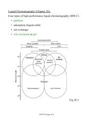
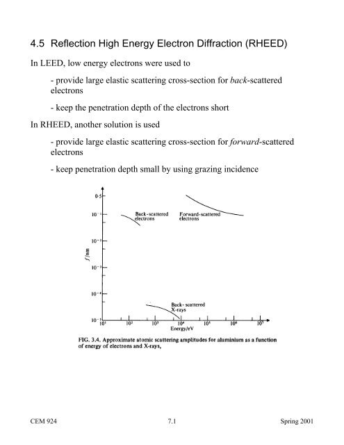
4.5 <strong>Reflection</strong> High Energy Electron Diffraction (<strong>RHEED</strong>)In LEED, low <strong>energy</strong> <strong>electron</strong>s were used to- provide large elastic scattering cross-section for back-scattered<strong>electron</strong>s- keep the penetration depth of the <strong>electron</strong>s shortIn <strong>RHEED</strong>, another solution is used- provide large elastic scattering cross-section for forward-scattered<strong>electron</strong>s- keep penetration depth small by using grazing incidenceCEM 924 7.1 Spring 2001
4.5.1 InstrumentationElectrons 5-100 keV directed towards sample at very near θ i 90° - keeps evenlong-pathlength (<strong>high</strong>-<strong>energy</strong>) <strong>electron</strong>s in near-surface regionForward-diffracted <strong>electron</strong>s strike phosphor screenGrid used to repel secondary and inelastically scattered <strong>electron</strong>s4.5.2 Basic Theory of <strong>RHEED</strong>Theory very similar to LEED (Ewald sphere) but incident wavevector rk nowvery large:Example: 50 keV <strong>electron</strong> incident in [110] direction of Cu (a 0 =3.56 Å)λ =2m(eV)= 5.5x10 −12 m= 0.055 Årk = 2π λ= 114 Å −1and reciprocal lattice spacing isCEM 924 7.2 Spring 2001
a = 2πd=2π3.56 Å / 2= 2.49 Å −1Draw Ewald sphere for an incidence angle of 88°:k'EwaldspherePart of Ewald sphere(00)k(00)k'Surface2θkgConsequences?(1) Ewald sphere crosses many lattice rods - many spots separated by small<strong>diffraction</strong> angle differencesbut few near grazing exit angles - usually only see (00) beam and perhaps(1 0) beam(2) Crossing of Ewald sphere with lattice (condition for <strong>diffraction</strong>) rod verypoorly defined - <strong>RHEED</strong> spots are broadened into "vertical" streaksNow <strong>diffraction</strong> out of incidence plane (determined by periodicity orthogonalto incidence plane) becomes importantThe <strong>RHEED</strong> pattern can be used to measure surface periodicity orthogonal toincidence plane by measuring the separation between the streaks:CEM 924 7.3 Spring 2001
tanθ = S L ≈ sin θsince θ is smalld ≈ ⎜⎛ h 2 + l⎝2 ⎞⎟ ⋅λ⋅ S ⎠ LIf information about periodicity in plane of incidence is required, θ i must beincreased so that the Ewald sphere cuts several reciprocal lattice rods- streaks then become rows of (blurred) spotsIntensity versus θ i - I(θ I ) "rocking curves" - can be used with dynamical theoryto extract detailed atomic spacingCEM 924 7.4 Spring 2001
- theory less well developed than LEED- includes many more multiple scattering events- includes many more inelastic events- quantitative <strong>RHEED</strong> usually not performed4.5.3 Applications of <strong>RHEED</strong><strong>RHEED</strong> is very sensitive to surface roughness on 100-1000 Å scaleSince pathlength of <strong>RHEED</strong> <strong>electron</strong> is <strong>high</strong>, <strong>electron</strong> may pass through asmall surface feature and cause true bulk-like <strong>diffraction</strong>CEM 924 7.5 Spring 2001
Such bulk <strong>diffraction</strong>- reduces intensity in <strong>RHEED</strong> streaks- causes sharp spots in <strong>RHEED</strong> patternCan use <strong>RHEED</strong> to follow growth of one material on another (epitaxy) - As,Ga molecular beams on GaAs(001) surfaceCEM 924 7.6 Spring 2001
In this case, growth proceeds by Franck-Van der Merwe growth mode (layerby-layer)Experimental arrangement of <strong>RHEED</strong> (compared with LEED) makes itespecially suited to molecular beam epitaxy (MBE) and metal-organicchemical vapor deposition (MOCVD) studies<strong>RHEED</strong> used widely in semiconductor growth industry4.6 X-ray Techniques for Surface Structure DeterminationX-ray absorption process very similar to optical absorption - obeys Beers Lawx-rays are energetic enough to ionize both valence <strong>electron</strong>s and somecore <strong>electron</strong>sAbsorption characterized by series of "absorption edges" corresponding toionization of each core levelEach edge denoted by x-ray notation and is made up of several closely-spacededgesCEM 924 7.7 Spring 2001
"Atomic notation": n l j j = l ± sAtomic NotationX-ray Notation1s K 12s L 12p 1/2 L 22p 3/2 L 33s M 13p 1/2 M 23p 3/2 M 33d 3/2 M 43d 5/2 M 5Position of edge slightly sensitive to "chemical environment" of atom -oxidation state, bonding environment - producing a chemical shiftAbsorption is same as optical absorptionI = I 0 ⋅exp( −α(hν)⋅ l)A = Ψ i µ Ψ f2Absorption α(hν) generally strongest at absorption edge then decreasesFine structure (small intensity modulation) appears in x-ray absorptionspectrum above edge(1) Extended X-ray Absorption Fine Structure (EXAFS)(2) Near-Edge X-ray Absorption Fine Structure (NEXAFS) or X-rayAbsorption Near-Edge Structure (XANES)CEM 924 7.8 Spring 2001
4.6.1 Extended X-ray Absorption Fine Structure (EXAFS)Effect is due to interference between outgoing <strong>electron</strong> wave (photo<strong>electron</strong>)and part of outgoing <strong>electron</strong> wave scattered by neighboring atoms- oscillations in x-ray intensity 50~200 eV from absorption edgeCEM 924 7.9 Spring 2001
- does not occur for isolated atoms- outgoing photo<strong>electron</strong> (KE > 50 eV) behaves like free <strong>electron</strong>- most interference from nearest neighbors- sensitive to short-range order (unlike <strong>diffraction</strong>) - works foramorphous, polycrystalline, glassy materials, liquids- can select absorption edge for one particular species (C, O, N… )If we assume that outgoing and back-scattered <strong>electron</strong>s can be treated as planewaves, constructive interference occurs whenn⋅ λ = 2⋅rDestructive interference will occur whenn⋅ λ2 = 2⋅rAt intermediate values of λ, intermediate interference results that affects theintensity of the outgoing wave.Energy of outgoing photo<strong>electron</strong> (at absorption edge threshold photo<strong>electron</strong>has zero KE)SinceE = hν photon − hν thresholdE = 1 2 m⋅c2 = p22mandp = h λwe can writeCEM 924 7.10 Spring 2001
E = hν photon − hν thresholdλ =h( 2m[ hν photon − hν threshold ]) 1/2Constructive interference occurs whenever,nλ = 2⋅rn =2⋅r ⋅ 2m hν photon − hν thresholdh( [ ]) 1/2where n is really a measure of the "degree of interference"Interference modulates amplitude of Ψ f and hence modulates x-ray absorbanceA = Ψ i µ Ψ f2- when n is an integer, constructive interference between outgoing andscattered photo<strong>electron</strong> wave causes strong x-ray absorption- when n is integer + half, destructive interference between outgoingand scattered photo<strong>electron</strong> causing reduced x-ray absorptionOther features to note:(1) period of oscillations increase as hν increases above hν threshold(2) period of oscillations becomes longer if r is decreased(3) intensity of oscillations increases with more scatterers at distance rCEM 924 7.11 Spring 2001
Most often raw α(hν) versus hν data is re-plotted versus wavevector k (=2·π/λ)nλ =2⋅r ⋅ ( 2m[ hν photon − hν threshold ]) ( [ ]) 1/2k= 2m hν photon − hν threshold2⋅π⋅hh( ) 1/2=0.5123 hν photon − hν threshold2⋅π1/2= 2⋅r⋅kwhere k is in Å -1 and hν in eV. Fourier-transform of α(hν) versus k givesnearest-neighbor distances (and intensity gives number of atoms)CEM 924 7.12 Spring 2001
CEM 924 7.13 Spring 2001
4.6.2 Instrumentation for EXAFSTunable x-ray source (<strong>electron</strong> storage ring - synchrotron)- pulsed, plane polarized outputX-ray monochromator (< few eV resolution)Detector for I and I 0 - ion chamber (total ion current α intensity)4.6.3 Surface EXAFS (SEXAFS)Basic problem in making EXAFS surface sensitive is removing contributionfrom bulk absorptiond# Bulk ~ (V x ρ/AW) x N# Surface ~ 6 x (1/d) 2AFor 1 x 1 x 1 cm 3 Au: (NN distance = 2.89 Å, AW = 197 g·mol -1 , ρ = 19.3g·cm -3 ) # bulk atoms = 6x10 22 , number surface atoms = 6x10 15 (0.1 ppm)CEM 924 7.14 Spring 2001
The conventional EXAFS technique can be made more surface sensitive bygrazing incidence- by varying incidence angle, surface sensitivity can be altered from nmto mm- can detect reflected beam directly or x-ray fluorescence (α absorption)- photons have long pathlength in solids (1-100 µm)One way is to measure x-ray fluorescence from atom known to be present onsurface only- fluorescence from O or C atoms for c(2x2)CO-Ni(100)Another way is to measure low <strong>energy</strong> photo<strong>electron</strong>s coming from surfaceLow <strong>energy</strong> <strong>electron</strong>s have short inelastic mean free path (IMFP), λ, in solids(used in LEED to give surface sensitivity, remember?)CEM 924 7.15 Spring 2001
Electrons of KE ~100 eV have shortest IMFP so are most surface sensitiveMay collect- total <strong>electron</strong> yield- Auger <strong>electron</strong> yieldLow signal intensitiesLong data collection time - require UHV to minimize surface contaminationduring data acquisition4.7 Near-Edge X-ray Absorption Fine Structure (NEXAFS orXANES)Fine structure less than ~50 eV from absorption edgeIn EXAFS, interaction between outgoing wave and scatterer strong - singlescattering events dominateIn NEXAFS, interaction between outgoing wave and scatterer weak - multiplescattering events dominateCEM 924 7.16 Spring 2001
Need dynamical calculations to determine origin of fine structure peaksFor molecules adsorbed on surfaces, often see additional absorption features(resonances) due to intramolecular excitation (π → π*, σ → σ∗)For CO on Ni(100)A - σ → 2π* (allowed when E vector perpendicular to -C≡O bond)B - σ → σ∗ (allowed when E vector parallel to -C≡O bond)Alteration of incidence angle can be used to determine alignment of adsorbatebondsCEM 924 7.17 Spring 2001
4.8 Summary<strong>RHEED</strong> provides similar information to LEEDSurface sensitivity can be varied somewhat by changing incidence angle (20->500 Å)Very simple, inexpensive instrumentation amenable to MBE, MOCVD andfilm growth situationsRapid for simple analysisRocking curves can be used with theory to measure atomic positions butdifficultBUT<strong>RHEED</strong> theory not fully developed (many body multiple scattering theory)Only information in 1-D without azimuthal crystal rotationSensitive to surface roughness - not intrinsically surface sensitiveX-ray scattering techniques sensitive to short range order - accurate nearestneighbor distancesWorks for disordered materials unlike <strong>diffraction</strong>Information about chemical environmentIntrinsically bulk sensitive - can be made surface sensitive by- grazing incidence- using core edge of adsorbate- collecting low <strong>energy</strong> <strong>electron</strong>sSimple instrumentation (in principle)NEXAFS resonances useful for determining orientation of adsorbateCEM 924 7.18 Spring 2001
BUTRequires synchrotron for tunable x-rays - very expensiveComplex theory needed to fully interpret data- single scattering (EXAFS)- multiple scattering (NEXAFS/XANES)CEM 924 7.19 Spring 2001