NEETS Module 8, Chapter 1
NEETS Module 8, Chapter 1
NEETS Module 8, Chapter 1

Create successful ePaper yourself
Turn your PDF publications into a flip-book with our unique Google optimized e-Paper software.
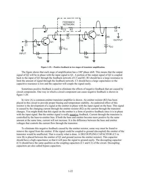
Figure 1-19.—Positive feedback in two stages of transistor amplification.The figure shows that each stage of amplification has a 180º phase shift. This means that the outputsignal of Q2 will be in phase with the input signal to Q1. A portion of the output signal of Q2 is coupledback to the input of Q1 through the feedback network of C3 and R3. R3 should have a large resistance tolimit the amount of signal through the feedback network. C3 should have a large capacitance so thecapacitive reactance is low and the capacitor will couple the signal easily.Sometimes positive feedback is used to eliminate the effects of negative feedback that are caused bycircuit components. One way in which a circuit component can cause negative feedback is shown infigure 1-20.In view (A) a common-emitter transistor amplifier is shown. An emitter resistor (R2) has beenplaced in this circuit to provide proper biasing and temperature stability. An undesired effect of thisresistor is the development of a signal at the emitter in phase with the input signal on the base. This signalis caused by the changing current through the emitter resistor (R2) as the current through the transistorchanges. You might think that this signal on the emitter is a form of positive feedback since it is in phasewith the input signal. But the emitter signal is really negative feedback. Current through the transistor iscontrolled by the base-to-emitter bias. If both the base and emitter become more positive by the sameamount at the same time, current will not increase. It is the difference between the base and emittervoltages that controls the current flow through the transistor.To eliminate this negative feedback caused by the emitter resistor, some way must be found toremove the signal from the emitter. If the signal could be coupled to ground (decoupled) the emitter of thetransistor would be unaffected. That is exactly what is done. A DECOUPLING CAPACITOR (C3 inview B) is placed between the emitter of Q1 and ground (across the emitter resistor). This capacitorshould have a high capacitance so that it will pass the signal to ground easily. The decoupling capacitor(C3) should have the same qualities as the coupling capacitors (C1 and C2) of the circuit. Decouplingcapacitors are also called bypass capacitors.1-22