NEETS Module 8, Chapter 1
NEETS Module 8, Chapter 1
NEETS Module 8, Chapter 1
You also want an ePaper? Increase the reach of your titles
YUMPU automatically turns print PDFs into web optimized ePapers that Google loves.
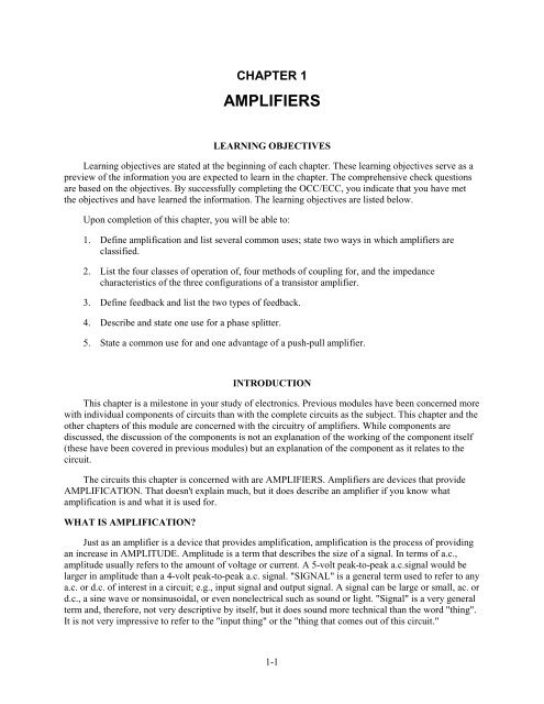
CHAPTER 1AMPLIFIERSLEARNING OBJECTIVESLearning objectives are stated at the beginning of each chapter. These learning objectives serve as apreview of the information you are expected to learn in the chapter. The comprehensive check questionsare based on the objectives. By successfully completing the OCC/ECC, you indicate that you have metthe objectives and have learned the information. The learning objectives are listed below.Upon completion of this chapter, you will be able to:1. Define amplification and list several common uses; state two ways in which amplifiers areclassified.2. List the four classes of operation of, four methods of coupling for, and the impedancecharacteristics of the three configurations of a transistor amplifier.3. Define feedback and list the two types of feedback.4. Describe and state one use for a phase splitter.5. State a common use for and one advantage of a push-pull amplifier.INTRODUCTIONThis chapter is a milestone in your study of electronics. Previous modules have been concerned morewith individual components of circuits than with the complete circuits as the subject. This chapter and theother chapters of this module are concerned with the circuitry of amplifiers. While components arediscussed, the discussion of the components is not an explanation of the working of the component itself(these have been covered in previous modules) but an explanation of the component as it relates to thecircuit.The circuits this chapter is concerned with are AMPLIFIERS. Amplifiers are devices that provideAMPLIFICATION. That doesn't explain much, but it does describe an amplifier if you know whatamplification is and what it is used for.WHAT IS AMPLIFICATION?Just as an amplifier is a device that provides amplification, amplification is the process of providingan increase in AMPLITUDE. Amplitude is a term that describes the size of a signal. In terms of a.c.,amplitude usually refers to the amount of voltage or current. A 5-volt peak-to-peak a.c.signal would belarger in amplitude than a 4-volt peak-to-peak a.c. signal. "SIGNAL" is a general term used to refer to anya.c. or d.c. of interest in a circuit; e.g., input signal and output signal. A signal can be large or small, ac. ord.c., a sine wave or nonsinusoidal, or even nonelectrical such as sound or light. "Signal" is a very generalterm and, therefore, not very descriptive by itself, but it does sound more technical than the word "thing".It is not very impressive to refer to the "input thing" or the "thing that comes out of this circuit."1-1
Perhaps the concept of the relationship of amplifier-amplification-amplitude will be clearer if youconsider a parallel situation (an analogy). A magnifying glass is a magnifier. As such, it providesmagnification which is an increase in the magnitude (size) of an object. This relationship of magnifiermagnification-magnitudeis the same as the relationship of amplifier-amplification-amplitude. Theanalogy is true in one other aspect as well. The magnifier does not change the object that is beingmagnified; it is only the image that is larger, not the object itself. With the amplifier, the output signaldiffers in amplitude from the input signal, but the input signal still exists unchanged. So, the object (inputsignal) and the magnifier (amplifier) control the image (output signal).An amplifier can be defined as a device that enables an input signal to control an output signal. Theoutput signal will have some (or all) of the characteristics of the input signal but will generally be largerthan the input signal in terms of voltage, current, or power.USES OF AMPLIFICATIONMost electronic devices use amplifiers to provide various amounts of signal amplification. Sincemost signals are originally too small to control or drive the desired device, some amplification is needed.For example, the audio signal taken from a record is too small to drive a speaker, so amplification isneeded. The signal will be amplified several times between the needle of the record player and thespeaker. Each time the signal is amplified it is said to go through a STAGE of amplification. The audioamplifier shown connected between the turntable and speaker system in figure 1-1 contains several stagesof amplification.TURNTABLEAMPLIFIERSPEAKERNTS080101Figure 1-1.—Amplifier as used with turntable and speaker.Notice the triangle used in figure 1-1 to represent the amplifier. This triangle is the standard blockdiagram symbol for an amplifier.Another example of the use of an amplifier is shown in figure 1-2. In a radio receiver, the signalpicked up by the antenna is too weak (small) to be used as it is. This signal must be amplified before it issent to the detector. (The detector separates the audio signal from the frequency that was sent by thetransmitter. The way in which this is done will be discussed later in this training series.)1-2
ANTENNADETECTOR(SEPARATES AUDIO FROMRADIO FREQUENCY)AMPLIFIER(RADIO FREQUENCY)AMPLIFIER(AUDIO FREQUENCY)SPEAKERNTS080102Figure 1-2.—Amplifiers as used in radio receiver.The audio signal from the detector will then be amplified to make it large enough to drive thespeaker of the radio.Almost every electronic device contains at least one stage of amplification, so you will be seeingamplifiers in many devices that you work on. Amplifiers will also be used in most of the <strong>NEETS</strong> modulesthat follow this one.Q-1. What is amplification?Q-2. Does an amplifier actually change an input signal? Why or why not?Q-3. Why do electronic devices use amplifiers?CLASSIFICATION OF AMPLIFIERSMost electronic devices use at least one amplifier, but there are many types of amplifiers. Thismodule will not try to describe all the different types of amplifiers. You will be shown the generalprinciples of amplifiers and some typical amplifier circuits.Most amplifiers can be classified in two ways. The first classification is by their function. Thismeans they are basically voltage amplifiers or power amplifiers. The second classification is by theirfrequency response. In other words what frequencies are they designed to amplify?If you describe an amplifier by these two classifications (function and frequency response) you willhave a good working description of the amplifier. You may not know what the exact circuitry is, but youwill know what the amplifier does and the frequencies that it is designed to handle.VOLTAGE AMPLIFIERS AND POWER AMPLIFIERSAll amplifiers are current-control devices. The input signal to an amplifier controls the current outputof the amplifier. The connections of the amplifying device (electron tube, transistor, magnetic amplifier,1-3
etc.) and the circuitry of the amplifier determine the classification. Amplifiers are classified as voltage orpower amplifiers.A VOLTAGE AMPLIFIER is an amplifier in which the output signal voltage is larger than the inputsignal voltage. In other words, a voltage amplifier amplifies the voltage of the input signal.A POWER AMPLIFIER is an amplifier in which the output signal power is greater than the inputsignal power. In other words, a power amplifier amplifies the power of the input signal. Most poweramplifiers are used as the final amplifier (stage of amplification) and control (or drive) the output device.The output device could be a speaker, an indicating device, an antenna, or the heads on a tape recorder.Whatever the device, the power to make it work (or drive it) comes from the final stage of amplificationwhich is a power amplifier.Figure 1-3 shows a simple block diagram of a voltage amplifier with its input and output signals anda power amplifier with its input and output signals. Notice that in view (A) the output signal voltage islarger than the input signal voltage. Since the current values for the input and output signals are notshown, you cannot tell if there is a power gain in addition to the voltage gain.INOUTINPUT SIGNAL200 mV PEAK-TO-PEAKAOUTPUT SIGNAL4 V PEAK-TO-PEAKINOUTINPUT SIGNAL10 V PEAK-TO-PEAK100 mA (1W OF POWER)OUTPUT SIGNAL5 V PEAK-TO-PEAK2 A (10W OF POWER)BVOLTAGE AND POWER AMPLIFIERSNTS080103Figure 1-3.—Diagram of voltage and power amplifiers.In view (B) of the figure the output signal voltage is less than the input signal voltage. As a voltageamplifier, this circuit has a gain of less than 1. The output power, however, is greater than the inputpower. Therefore, this circuit is a power amplifier.The classification of an amplifier as a voltage or power amplifier is made by comparing thecharacteristics of the input and output signals. If the output signal is larger in voltage amplitude than theinput signal, the amplifier is a voltage amplifier. If there is no voltage gain, but the output power is greaterthan the input power, the amplifier is a power amplifier.1-4
FREQUENCY RESPONSE OF AMPLIFIERSIn addition to being classified by function, amplifiers are classified by frequency response. Thefrequency response of an amplifier refers to the band of frequencies or frequency range that the amplifierwas designed to amplify.You may wonder why the frequency response is important. Why doesn't an amplifier designed toamplify a signal of 1000 Hz work just as well at 1000 MHz? The answer is that the components of theamplifier respond differently at different frequencies. The amplifying device (electron tube, transistor,magnetic amplifier, etc.) itself will have frequency limitations and respond in different ways as thefrequency changes. Capacitors and inductors in the circuit will change their reactance as the frequencychanges. Even the slight amounts of capacitance and inductance between the circuit wiring and othercomponents (interelectrode capacitance and self-inductance) can become significant at high frequencies.Since the response of components varies with the frequency, the components of an amplifier are selectedto amplify a certain range or band of frequencies.NOTE: For explanations of interelectrode capacitance and self-inductance see <strong>NEETS</strong> <strong>Module</strong>s 2—Introduction to Alternating Current and Transformers; 6—Introduction to Electronic Emission, Tubes,and Power Supplies; and 7—Introduction to Solid-State Devices and Power Supplies.The three broad categories of frequency response for amplifiers are AUDIO AMPLIFIER, RFAMPLIFIER, and VIDEO AMPLIFIER.An audio amplifier is designed to amplify frequencies between 15 Hz and 20 kHz. Any amplifier thatis designed for this entire band of frequencies or any band of frequencies contained in the audio range isconsidered to be an audio amplifier.In the term rf amplifier, the "rf" stands for radio frequency. These amplifiers are designed to amplifyfrequencies between 10 kHz and 100,000 MHz. A single amplifier will not amplify the entire rf range, butany amplifier whose frequency band is included in the rf range is considered an rf amplifier.A video amplifier is an amplifier designed to amplify a band of frequencies from 10 Hz to 6 MHz.Because this is such a wide band of frequencies, these amplifiers are sometimes called WIDE-BANDAMPLIFIERS. While a video amplifier will amplify a very wide band of frequencies, it does not have thegain of narrower-band amplifiers. It also requires a great many more components than a narrow-bandamplifier to enable it to amplify a wide range of frequencies.Q-4. In what two ways are amplifiers classified?Q-5. What type of amplifier would be used to drive the speaker system of a record player?Q-6. What type of amplifier would be used to amplify the signal from a radio antenna?TRANSISTOR AMPLIFIERSA transistor amplifier is a current-control device. The current in the base of the transistor (which isdependent on the emitter-base bias) controls the current in the collector. A vacuum-tube amplifier is alsoa current-control device. The grid bias controls the plate current. These facts are expanded upon in<strong>NEETS</strong> <strong>Module</strong> 6, Introduction to Electronic Emission, Tubes and Power Supplies, and <strong>Module</strong> 7,Introduction to Solid-State Devices and Power Supplies.1-5
You might hear that a vacuum tube is a voltage-operated device (since the grid does not need to drawcurrent) while the transistor is a current-operated device. You might agree with this statement, but boththe vacuum tube and the transistor are still current-control devices. The whole secret to understandingamplifiers is to remember that fact. Current control is the name of the game. Once current is controlledyou can use it to give you a voltage gain or a power gain.This chapter will use transistor amplifiers to present the concepts and principles of amplifiers. Theseconcepts apply to vacuum-tube amplifiers and, in most cases, magnetic amplifiers as well as transistoramplifiers. If you wish to study the vacuum-tube equivalent circuits of the transistor circuits presented, anexcellent source is the EIMB, NAVSEA 0967-LP-000-0120, Electronics Circuits.The first amplifier concept that is discussed is the "class of operation" of an amplifier.AMPLIFIER CLASSES OF OPERATIONThe class of operation of an amplifier is determined by the amount of time (in relation to the inputsignal) that current flows in the output circuit. This is a function of the operating point of the amplifyingdevice. The operating point of the amplifying device is determined by the bias applied to the device.There are four classes of operation for an amplifier. These are: A, AB, B and C. Each class of operationhas certain uses and characteristics. No one class of operation is "better" than any other class. Theselection of the "best" class of operation is determined by the use of the amplifying circuit. The best classof operation for a phonograph is not the best class for a radio transmitter.Class A OperationA simple transistor amplifier that is operated class A is shown in figure 1-4. Since the output signalis a 100% (or 360º) copy of the input signal, current in the output circuit must flow for 100% of the inputsignal time. This is the definition of a class A amplifier. Amplifier current flows for 100% of the inputsignal.+VCCR1OUTQ1INR2V EENTS080104Figure 1-4.—A simple class A transistor amplifier.The class A amplifier has the characteristics of good FIDELITY and low EFFICIENCY. Fidelitymeans that the output signal is just like the input signal in all respects except amplitude. It has the same1-6
shape and frequency. In some cases, there may be a phase difference between the input and output signal(usually 180º), but the signals are still considered to be "good copies." If the output signal is not like theinput signal in shape or frequency, the signal is said to be DISTORTED. DISTORTION is any undesiredchange in a signal from input to output.The efficiency of an amplifier refers to the amount of power delivered to the output compared to thepower supplied to the circuit. Since every device takes power to operate, if the amplifier operates for 360ºof input signal, it uses more power than if it only operates for 180º of input signal. If the amplifier usesmore power, less power is available for the output signal and efficiency is lower. Since class A amplifiersoperate (have current flow) for 360º of input signal, they are low in efficiency. This low efficiency isacceptable in class A amplifiers because they are used where efficiency is not as important as fidelity.Class A B OperationIf the amplifying device is biased in such a way that current flows in the device for 51% - 99% of theinput signal, the amplifier is operating class AB. A simple class AB amplifier is shown in figure 1-5.+V CCR1OUTQ1INR2V EENTS080105Figure 1-5.—A simple class AB transistor amplifier.Notice that the output signal is distorted. The output signal no longer has the same shape as the inputsignal. The portion of the ou tput signal that appears to be cut off is caused by the lack of current throughthe transistor. When the emitter becomes positive enough, the transistor cannot conduct because the baseto-emitterjunction is no longer forward biased. Any further increase in input signal will not cause anincrease in output signal voltage.Class AB amplifiers have better efficiency and poorer fidelity than class A amplifiers. They are usedwhen the output signal need not be a complete reproduction of the input signal, but both positive andnegative portions of the input signal must be available at the output.Class AB amplifiers are usually defined as amplifiers operating between class A and class B becauseclass A amplifiers operate on 100% of input signal and class B amplifiers (discussed next) operate on50% of the input signal. Any amplifier operating between these two limits is operating class AB.1-7
Class B OperationAs was stated above, a class B amplifier operates for 50% of the input signal. A simple class Bamplifier is shown in figure 1-6.+V CCR1OUTQ1VBBINR2VEEFigure 1-6.—A simple class B transistor amplifier.In the circuit shown in figure 1-6, the base-emitter bias will not allow the transistor to conductwhenever the input signal becomes positive. Therefore, only the negative portion of the input signal isreproduced in the output signal. You may wonder why a class B amplifier would be used instead of asimple rectifier if only half the input signal is desired in the output. The answer to this is that the rectifierdoes not amplify. The output signal of a rectifier cannot be higher in amplitude than the input signal. Theclass B amplifier not only reproduces half the input signal, but amplifies it as well.Class B amplifiers are twice as efficient as class A amplifiers since the amplifying device onlyconducts (and uses power) for half of the input signal. A class B amplifier is used in cases where exactly50% of the input signal must be amplified. If less than 50% of the input signal is needed, a class Camplifier is used.Class C OperationNTS080106Figure 1-7 shows a simple class C amplifier. Notice that only a small portion of the input signal ispresent in the output signal. Since the transistor does not conduct except during a small portion of theinput signal, this is the most efficient amplifier. It also has the worst fidelity. The output signal bears verylittle resemblance to the input signal.1-8
+V CCR1OUTQ1VBBINR2VEEFigure 1-7.—A simple class C transistor amplifier.Class C amplifiers are used where the output signal need only be present during part of one-half ofthe input signal. Any amplifier that operates on less than 50% of the input signal is operated class C.Q-7. What determines the class of operation of an amplifier?Q-8. What are the four classes of operation of a transistor amplifier?Q-9. If the output of a circuit needs to be a complete representation of one-half of the input signal,what class of operation is indicated?Q-10. Why is class C operation more efficient than class A operation?Q-11. What class of operation has the highest fidelity?AMPLIFIER COUPLINGNTS080107Earlier in this module it was stated that almost every electronic device contains at least one stage ofamplification. Many devices contain several stages of amplification and therefore several amplifiers.Stages of amplification are added when a single stage will not provide the required amount ofamplification. For example, if a single stage of amplification will provide a maximum gain of 100 and thedesired gain from the device is 1000, two stages of amplification will be required. The two stages mighthave gains of 10 and 100, 20 and 50, or 25 and 40. (The overall gain is the product of the individualstages-10 × 100 = 20 × 50 = 25 × 40 = 1000.)Figure 1-8 shows the effect of adding stages of amplification. As stages of amplification are added,the signal increases and the final output (from the speaker) is increased.1-9
TURNTABLEAMPLI-FIERSPEAKERTURNTABLEAMPLI-FIERAMPLI-FIERSPEAKERSPEAKERTURNTABLEAMPLI-FIERAMPLI-FIERAMPLI-FIERSPEAKERNTS080108Figure 1-8.—Adding stages of amplification.Whether an amplifier is one of a series in a device or a single stage connected between two otherdevices (top view, figure 1-8), there must be some way for the signal to enter and leave the amplifier. Theprocess of transferring energy between circuits is known as COUPLING. There are various ways ofcoupling signals into and out of amplifier circuits. The following is a description of some of the morecommon methods of amplifier coupling.Direct CouplingThe method of coupling that uses the least number of circuit elements and that is, perhaps, the easiestto understand is direct coupling. In direct coupling the output of one stage is connected directly to theinput of the following stage. Figure 1-9 shows two direct-coupled transistor amplifiers.1-10
V BB7VQ213VOUTPUTR1Q1R2R3INPUTR4R5R6Vcc6V10V15VNTS080109Figure 1-9.—Direct-coupled transistor amplifier.Notice that the output (collector) of Q1 is connected directly to the input (base) of Q2. The networkof R4, R5, and R6 is a voltage divider used to provide the bias and operating voltages for Q1 and Q2. Theentire circuit provides two stages of amplification.Direct coupling provides a good frequency response since no frequency-sensitive components(inductors and capacitors) are used. The frequency response of a circuit using direct coupling is affectedonly by the amplifying device itself.Direct coupling has several disadvantages, however. The major problem is the power supplyrequirements for direct-coupled amplifiers. Each succeeding stage requires a higher voltage. The load andvoltage divider resistors use a large amount of power and the biasing can become very complicated. Inaddition, it is difficult to match the impedance from stage to stage with direct coupling. (Impedancematching is covered a little later in this chapter.)The direct-coupled amplifier is not very efficient and the losses increase as the number of stagesincrease. Because of the disadvantages, direct coupling is not used very often.RC CouplingThe most commonly used coupling in amplifiers is RC coupling. An RC-coupling network is shownin figure 1-10.1-11
Q2OUTPUTQ1R1C1R2INPUT+ VccNTS080110Figure 1-10.—RC-coupled transistor amplifier.The network of R1, R2, and C1 enclosed in the dashed lines of the figure is the coupling network.You may notice that the circuitry for Q1 and Q2 is incomplete. That is intentional so that you canconcentrate on the coupling network.R1 acts as a load resistor for Q1 (the first stage) and develops the output signal of that stage. Do youremember how a capacitor reacts to ac and dc? The capacitor, C1, "blocks" the dc of Q1's collector, but"passes" the ac output signal. R2 develops this passed, or coupled, signal as the input signal to Q2 (thesecond stage). This arrangement allows the coupling of the signal while it isolates the biasing of eachstage. This solves many of the problems associated with direct coupling.RC coupling does have a few disadvantages. The resistors use dc power and so the amplifier has lowefficiency. The capacitor tends to limit the low-frequency response of the amplifier and the amplifyingdevice itself limits the high-frequency response. For audio amplifiers this is usually not a problem;techniques for overcoming these frequency limitations will be covered later in this module.Before you move on to the next type of coupling, consider the capacitor in the RC coupling. Youprobably remember that capacitive reactance (X C) is determined by the following formula:1X C = 2πfCThis explains why the low frequencies are limited by the capacitor. As frequency decreases, X Cincreases. This causes more of the signal to be "lost" in the capacitor.The formula for X C also shows that the value of capacitance (C) should be relatively high so thatcapacitive reactance (X C ) can be kept as low as possible. So, when a capacitor is used as a couplingelement, the capacitance should be relatively high so that it will couple the entire signal well and notreduce or distort the signal.Impedance CouplingImpedance coupling is very similar to RC coupling. The difference is the use of an impedance device(a coil) to replace the load resistor of the first stage.1-12
Figure 1-11 shows an impedance-coupling network between two stages of amplification. L1 is theload for Q1 and develops the output signal of the first stage. Since the d.c. resistance of a coil is low, theefficiency of the amplifier stage is increased. The amount of signal developed in the output of the stagedepends on the inductive reactance of L1. Remember the formula for inductive reactance:X L = 2πfLQ2OUTPUTQ1L1C1R2INPUT+ VccNTS080111Figure 1-11.—Impedance-coupled transistor amplifier.The formula shows that for inductive reactance to be large, either inductance or frequency or bothmust be high. Therefore, load inductors should have relatively large amounts of inductance and are mosteffective at high frequencies. This explains why impedance coupling is usually not used for audioamplifiers.The rest of the coupling network (C1 and R1) functions just as their counterparts (C1 and R2) in theRC-coupling network. C1 couples the signal between stages while blocking the d.c. and R1 develops theinput signal to the second stage (Q2).Transformer CouplingFigure 1-12 shows a transformer-coupling network between two stages of amplification. Thetransformer action of T1 couples the signal from the first stage to the second stage. In figure 1-12, theprimary of T1 acts as the load for the first stage (Q1) and the secondary of T1 acts as the developingimpedance for the second stage (Q2). No capacitor is needed because transformer action couples thesignal between the primary and secondary of T1.1-13
Q1INPUTQ2T1+ V CCNTS080112OUTPUTFigure 1-12.—Transformer-coupled transistor amplifier.The inductors that make up the primary and secondary of the transformer have very little dcresistance, so the efficiency of the amplifiers is very high. Transformer coupling is very often used for thefinal output (between the final amplifier stage and the output device) because of the impedance-matchingqualities of the transformer. The frequency response of transformer-coupled amplifiers is limited by theinductive reactance of the transformer just as it was limited in impedance coupling.Q-12. What is the purpose of an amplifier-coupling network?Q-13. What are four methods of coupling amplifier stages?Q-14. What is the most common form of coupling?Q-15. What type coupling is usually used to couple the output from a power amplifier?Q-16. What type coupling would be most useful for an audio amplifier between the first and secondstages?Q-17. What type of coupling is most effective at high frequencies?IMPEDANCE CONSIDERATIONS FOR AMPLIFIERSIt has been mentioned that efficiency and impedance are important in amplifiers. The reasons for thismay not be too clear. You have been shown that any amplifier is a current-control device. Now there aretwo other principles you should try to keep in mind. First, there is no such thing as "something fornothing" in electronics. That means every time you do something to a signal it costs something. It mightmean a loss in fidelity to get high power. Some other compromise might also be made when a circuit isdesigned. Regardless of the compromise, every stage will require and use power. This brings up thesecond principle-do things as efficiently as possible. The improvement and design of electronic circuits isan attempt to do things as cheaply as possible, in terms of power, when all the other requirements(fidelity, power output, frequency range, etc.) have been met.This brings us to efficiency. The most efficient device is the one that does the job with the least lossof power. One of the largest losses of power is caused by impedance differences between the output ofone circuit and the input of the next circuit. Perhaps the best way to think of an impedance difference(mismatch) between circuits is to think of different-sized water pipes. If you try to connect a one-inchwater pipe to a two-inch water pipe without an adapter you will lose water. You must use an adapter. A1-14
impedance-matching device is like that adapter. It allows the connection of two devices with differentimpedances without the loss of power.Figure 1-13 shows two circuits connected together. Circuit number 1 can be considered as an a.c.source (E S ) whose output impedance is represented by a resistor (R1). It can be considered as an a.c.source because the output signal is an a.c. voltage and comes from circuit number 1 through the outputimpedance. The input impedance of circuit number 2 is represented by a resistor in series with the source.The resistance is shown as variable to show what will happen as the input impedance of circuit number 2is changed.CIRCUIT NO.1OUTPUTIMPEDANCE1K ΩCIRCUIT NO. 2E S = 10VR1=1KΩR2R2I IER2PR1 PR2I100Ω9mA900mV82.6mW8.3mW200 Ω8.3mA1.67V69.4mW13.9mW500Ω1kΩ2k Ω5k Ω10kΩ6.7mA 3.33V 44.4mW 22.2mW5mA 5V 25mW 25mW3.3mA 6.67V 11.1mW 22.2mW1.7mA 8.33V 2.7mW 13.9mW.9mA 9.09V .9mW 8.3mWNTS0801I-11Figure 1-13.—Effect of impedance matching in the coupling of two circuits.The chart below the circuit shows the effect of a change in the input impedance of circuit number 2(R2) on current (I), signal voltage developed at the input of circuit number 2 (E R2 ), the power at the outputof circuit number 1 (P R1 ), and the power at the input to circuit number 2 (P R2 ).Two important facts are brought out in this chart. First, the power at the input to circuit number 2 isgreatest when the impedances are equal (matched). The power is also equal at the output of circuitnumber 1 and the input of circuit number 2 when the impedance is matched. The second fact is that thelargest voltage signal is developed at the input to circuit number 2 when its input impedance is muchlarger than the output impedance of circuit number 1. However, the power at the input of circuit number 21-15
is very low under these conditions. So you must decide what conditions you want in coupling two circuitstogether and select the components appropriately.Two important points to remember about impedance matching are as follows. (1) Maximum powertransfer requires matched impedance. (2) To get maximum voltage at the input of a circuit requires anintentional impedance mismatch with the circuit that is providing the input signal.Impedance Characteristics of Amplifier ConfigurationsNow that you have seen the importance of impedance matching the stages in an electronic device,you may wonder what impedance characteristics an amplifier has. The input and output impedances of atransistor amplifier depend upon the configuration of the transistor. In <strong>Module</strong> 7, Introduction toSolid-State Devices and Power Supplies, you were introduced to the three transistor configurations; thecommon emitter, the common base, and the common collector. Examples of these configurations andtheir impedance characteristics are shown in figure 1-14.MEDIUM INPUT Z500Ω- 1500ΩVCCMEDIUM OUTPUT Z30k Ω - 50k ΩINPUTV BBCOMMON EMITTERVCCHIGH OUTPUT Z250Ω- 550 ΩLOW INPUT Z30k Ω - 60k ΩINPUTV EECOMMON BASEVCCHIGH INPUT Z2Ω- 500ΩLOW OUTPUT Z50k Ω - 1500k ΩINPUTV EEOUTPUTCOMMON COLLECTORNTS080114Figure 1-14.—Transistor amplifier configurations and their impedance characteristics.NOTE: Only approximate impedance values are shown. This is because the exact impedance valueswill vary from circuit to circuit. The impedance of any particular circuit depends upon the device(transistor) and the other circuit components. The value of impedance can be computed by dividing thesignal voltage by the signal current. Therefore:1-16
Input Signal Impedance =Input Signal VoltageInput Signal CurrentandOutput Signal Impedance =Output Signal VoltageOutput Signal CurrentThe common-emitter configuration provides a medium input impedance and a medium outputimpedance. The common-base configuration provides a low input impedance and a high outputimpedance. The common-collector configuration provides a high input impedance and a low outputimpedance. The common-collector configuration is often used to provide impedance matching between ahigh output impedance and a low input impedance.If the amplifier stage is transformer coupled, the turns ratio of the transformer can be selected toprovide impedance matching. In <strong>NEETS</strong> <strong>Module</strong> 2, Introduction to Alternating Current andTransformers, you were shown the relationship between the turns ratio and the impedance ratio in atransformer. The relationship is expressed in the following formula:PSPSAs you can see, impedance matching between stages can be accomplished by a combination of theamplifier configuration and the components used in the amplifier circuit.Q-18. What impedance relationship between the output of one circuit and the input of another circuitwill provide the maximum power transfer?Q-19. If maximum current is desired at the input to a circuit, should the input impedance of that circuitbe lower than, equal to, or higher than the output impedance of the previous stage?Q-20. What are the input- and output-impedance characteristics of the three transistor configurations?Q-21. What transistor circuit configuration should be used to match a high output impedance to a lowinput impedance?Q-22. What type of coupling is most useful for impedance matching?NNPS=ZZWhere:N = Number of turns in the primaryN = Number of turns in the secondaryZ = Impedance of the primaryZ = Impedance of the secondaryPS1-17
AMPLIFIER FEEDBACKPerhaps you have been around a public address system when a squeal or high-pitched noise hascome from the speaker. Someone will turn down the volume and the noise will stop. That noise is anindication that the amplifier (at least one stage of amplification) has begun oscillating. Oscillation iscovered in detail in <strong>NEETS</strong> <strong>Module</strong> 9, Introduction to Wave-Generation and Wave-Shaping Circuits. Fornow, you need only realize that the oscillation is caused by a small part of the signal from the amplifieroutput being sent back to the input of the amplifier. This signal is amplified and again sent back to theinput where it is amplified again. This process continues and the result is a loud noise out of the speaker.The process of sending part of the output signal of an amplifier back to the input of the amplifier is calledFEEDBACK.There are two types of feedback in amplifiers. They are POSITIVE FEEDBACK, also calledREGENERATIVE FEEDBACK, and NEGATIVE FEEDBACK, also called DEGENERATIVEFEEDBACK. The difference between these two types is whether the feedback signal is in phase or out ofphase with the input signal.Positive feedback occurs when the feedback signal is in phase with the input signal. Figure 1-15shows a block diagram of an amplifier with positive feedback. Notice that the feedback signal is in phasewith the input signal. This means that the feedback signal will add to or "regenerate" the input signal. Theresult is a larger amplitude output signal than would occur without the feedback. This type of feedback iswhat causes the public address system to squeal as described above.FEEDBACKSIGNALFEED-BACKNETWORKINPUT SIGNALOUTPUT SIGNALNTS080115Figure 1-15.—Positive feedback in an amplifier.Figure 1-16 is a block diagram of an amplifier with negative feedback. In this case, the feedbacksignal is out of phase with the input signal. This means that the feedback signal will subtract from or"degenerate" the input signal. This results in a lower amplitude output signal than would occur withoutthe feedback.1-18
FEEDBACKSIGNALFEED-BACKNETWORKINPUTSIGNALOUTPUTSIGNALNTS080116Figure 1-16.—Negative feedback in an amplifier.Sometimes feedback that is not desired occurs in an amplifier. This happens at high frequencies andlimits the high-frequency response of an amplifier. Unwanted feedback also occurs as the result of somecircuit components used in the biasing or coupling network. The usual solution to unwanted feedback is afeedback network of the opposite type. For example, a positive feedback network would counteractunwanted, negative feedback.Feedback is also used to get the ideal input signal. Normally, the maximum output signal is desiredfrom an amplifier. The amount of the output signal from an amplifier is dependent on the amount of theinput signal. However, if the input signal is too large, the amplifying device will be saturated and/or cutoff during part of the input signal. This causes the output signal to be distorted and reduces the fidelity ofthe amplifier. Amplifiers must provide the proper balance of gain and fidelity.Figure 1-17 shows the way in which feedback can be used to provide the maximum output signalwithout a loss in fidelity. In view A, an amplifier has good fidelity, but less gain than it could have. Byadding some positive feedback, as in view B, the gain of the stage is increased. In view C, an amplifierhas so much gain and such a large input signal that the output signal is distorted. This distortion is causedby the amplifying device becoming saturated and cutoff. By adding a negative feedback system, as inview D, the gain of the stage is decreased and the fidelity of the output signal improved.NTS080117AFigure 1-17A.-Feedback uses in amplifiers.1-19
POSITIVEFEEDBACKNETWORKFigure 1-17B.—Feedback uses in amplifiers.NTS080117BNTS080117CFigure 1-17C.—Feedback uses in amplifiers.NEGATIVEFEEDBACKNETWORKFigure 1-17D.—Feedback uses in amplifiers.Positive and negative feedback are accomplished in many ways, depending on the reasons requiringthe feedback. A few of the effects and methods of accomplishing feedback are presented next.Positive FeedbackNTS080117DAs you have seen, positive feedback is accomplished by adding part of the output signal in phasewith the input signal. In a common-base transistor amplifier, it is fairly simple to provide positivefeedback. Since the input and output signals are in phase, you need only couple part of the output signalback to the input. This is shown in figure 1-18.1-20
The feedback network in this amplifier is made up of R2 and C2. The value of C2 should be large sothat the capacitive reactance (X C) will be low and the capacitor will couple the signal easily. (This is alsothe case with the input and output coupling capacitors C1 and C3.) The resistive value of R2 should belarge to limit the amount of feedback signal and to ensure that the majority of the output signal goes on tothe next stage through C3.FEEDBACKNETWORKR2C3C2Q1R3OUTPUTV CCC1R1INPUTV EENTS080118Figure 1-18.—Positive feedback in a transistor amplifier.A more common configuration for transistor amplifiers is the common-emitter configuration.Positive feedback is a little more difficult with this configuration because the input and output signals are180º out of phase. Positive feedback can be accomplished by feeding a portion of the output signal of thesecond stage back to the input of the first stage. This arrangement is shown in figure 1-19.1-21
Figure 1-19.—Positive feedback in two stages of transistor amplification.The figure shows that each stage of amplification has a 180º phase shift. This means that the outputsignal of Q2 will be in phase with the input signal to Q1. A portion of the output signal of Q2 is coupledback to the input of Q1 through the feedback network of C3 and R3. R3 should have a large resistance tolimit the amount of signal through the feedback network. C3 should have a large capacitance so thecapacitive reactance is low and the capacitor will couple the signal easily.Sometimes positive feedback is used to eliminate the effects of negative feedback that are caused bycircuit components. One way in which a circuit component can cause negative feedback is shown infigure 1-20.In view (A) a common-emitter transistor amplifier is shown. An emitter resistor (R2) has beenplaced in this circuit to provide proper biasing and temperature stability. An undesired effect of thisresistor is the development of a signal at the emitter in phase with the input signal on the base. This signalis caused by the changing current through the emitter resistor (R2) as the current through the transistorchanges. You might think that this signal on the emitter is a form of positive feedback since it is in phasewith the input signal. But the emitter signal is really negative feedback. Current through the transistor iscontrolled by the base-to-emitter bias. If both the base and emitter become more positive by the sameamount at the same time, current will not increase. It is the difference between the base and emittervoltages that controls the current flow through the transistor.To eliminate this negative feedback caused by the emitter resistor, some way must be found toremove the signal from the emitter. If the signal could be coupled to ground (decoupled) the emitter of thetransistor would be unaffected. That is exactly what is done. A DECOUPLING CAPACITOR (C3 inview B) is placed between the emitter of Q1 and ground (across the emitter resistor). This capacitorshould have a high capacitance so that it will pass the signal to ground easily. The decoupling capacitor(C3) should have the same qualities as the coupling capacitors (C1 and C2) of the circuit. Decouplingcapacitors are also called bypass capacitors.1-22
C2C1Q1R3OUTPUTR1R2VCCINPUTVBBAC2C1Q1R3OUTPUTR1R2C3VCCINPUTVBBBNTS080120Figure 1-20A-B.—Decoupling (bypass) capacitor in a transistor amplifier.Regardless of the method used to provide positive feedback in a circuit, the purpose is to increase theoutput signal amplitude.Negative FeedbackNegative feedback is accomplished by adding part of the output signal out of phase with the inputsignal. You have seen that an emitter resistor in a common-emitter transistor amplifier will develop anegative feedback signal. Other methods of providing negative feedback are similar to those methodsused to provide positive feedback. The phase relationship of the feedback signal and the input signal is theonly difference.Figure 1-21 shows negative feedback in a common-emitter transistor amplifier. The feedbacknetwork of C2 and R2 couples part of the output signal of Q1 back to the input. Since the output signal is180º out of phase with the input signal, this causes negative feedback.1-23
Figure 1-21.—Negative feedback in a transistor amplifier.Negative feedback is used to improve fidelity of an amplifier by limiting the input signal. Negativefeedback can also be used to increase the frequency response of an amplifier. The gain of an amplifierdecreases when the limit of its frequency response is reached. When negative feedback is used, thefeedback signal decreases as the output signal decreases. At the limits of frequency response of theamplifier the smaller feedback signal means that the effective gain (gain with feedback) is increased. Thiswill improve the frequency response of the amplifier.Q-23. What is feedback?Q-24. What are the two types of feedback?Q-25. What type feedback provides increased amplitude output signals?Q-26. What type feedback provides the best fidelity?Q-27. If the feedback signal is out of phase with the input signal, what type feedback is provided?Q-28. What type feedback is provided by an unbypassed emitter resistor in a common-emittertransistor amplifier?AUDIO AMPLIFIERSAn audio amplifier has been described as an amplifier with a frequency response from 15 Hz to 20kHz. The frequency response of an amplifier can be shown graphically with a frequency response curve.Figure 1-22 is the ideal frequency response curve for an audio amplifier. This curve is practically "flat"from 15 Hz to 20 kHz. This means that the gain of the amplifier is equal between 15 Hz and 20 kHz.Above 20 kHz or below 15 Hz the gain decreases or "drops off" quite rapidly. The frequency response ofan amplifier is determined by the components in the circuit.1-24
Figure 1-22.—Ideal frequency response curve for an audio amplifier.The difference between an audio amplifier and other amplifiers is the frequency response of theamplifier. In the next chapter of this module you will be shown the techniques and components used tochange and extend the frequency response of an amplifier.The transistor itself will respond quite well to the audio frequency range. No special components areneeded to extend or modify the frequency response.You have already been shown the purpose of all the components in a transistor audio amplifier. Inthis portion of the chapter, schematic diagrams of several audio amplifiers will be shown and thefunctions of each of the components will be discussed.SINGLE-STAGE AUDIO AMPLIFIERSThe first single-stage audio amplifier is shown in figure 1-23. This circuit is a class A,common-emitter, RC-coupled, transistor, audio amplifier. C1 is a coupling capacitor that couples theinput signal to the base of Q1. R1 is used to develop the input signal and provide bias for the base of Q1.R2 is used to bias the emitter and provide temperature stability for Q1. C2 is used to provide decoupling(positive feedback) of the signal that would be developed by R2. R3 is the collector load for Q1 anddevelops the output signal. C3 is a coupling capacitor that couples the output signal to the next stage. V CCrepresents the collector-supply voltage. Since the transistor is a common-emitter configuration, it providesvoltage amplification. The input and output signals are 180º out of phase. The input and output impedanceare both medium.1-25
Figure 1-23.—Transistor audio amplifier.There is nothing new presented in this circuit. You should understand all of the functions of thecomponents in this circuit. If you do not, look back at the various sections presented earlier in thischapter.The second single-stage audio amplifier is shown in figure 1-24. This circuit is a class A,common-source, RC-coupled, FET, audio amplifier. C1 is a coupling capacitor which couples the inputsignal to the gate of Q1. R1 is used to develop the input signal for the gate of Q1. R2 is used to bias thesource of Q1. C2 is used to decouple the signal developed by R2 (and keep it from affecting the source ofQ1). R3 is the drain load for Q1 and develops the output signal. C3 couples the output signal to the nextstage. V DD is the supply voltage for the drain of Q1. Since this is a common-source configuration, theinput and output signals are 180º out of phase.Figure 1-24.—FET audio amplifier.1-26
If you do not remember how a FET works, refer to <strong>NEETS</strong> <strong>Module</strong> 7 Introduction to Solid-StateDevices and Power Supplies.The third single-stage audio amplifier is shown in figure 1-25. This is a class A, common-emitter,transformer-coupled, transistor, audio amplifier. The output device (speaker) is shown connected to thesecondary winding of the transformer. C1 is a coupling capacitor which couples the input signal to thebase of Q1. R1 develops the input signal. R2 is used to bias the emitter of Q1 and provides temperaturestability. C2 is a decoupling capacitor for R2. R3 is used to bias the base of Q1. The primary of T1 is thecollector load for Q1 and develops the output signal. T1 couples the output signal to the speaker andprovides impedance matching between the output impedance of the transistor (medium) and theimpedance of the speaker (low).PHASE SPLITTERSFigure 1-25.—Single-stage audio amplifier.Sometimes it is necessary to provide two signals that are equal in amplitude but 180º out of phasewith each other. (You will see one use of these two signals a little later in this chapter.) The two signalscan be provided from a single input signal by the use of a PHASE SPLITTER. A phase splitter is a devicethat produces two signals that differ in phase from each other from a single input signal. Figure 1-26 is ablock diagram of a phase splitter.NTS080126Figure 1-26.—Block diagram of a phase splitter.One way in which a phase splitter can be made is to use a center-tapped transformer. As you mayremember from your study of transformers, when the transformer secondary winding is center-tapped,two equal amplitude signals are produced. These signals will be 180º out of phase with each other. So atransformer with a center-tapped secondary fulfills the definition of a phase splitter.1-27
A transistor amplifier can be configured to act as a phase splitter. One method of doing this is shownin figure 1-27.Figure 1-27.—Single-stage transistor phase splitter.C1 is the input signal coupling capacitor and couples the input signal to the base of Q1. R1 developsthe input signal. R2 and R3 develop the output signals. R2 and R3 are equal resistances to provide equalamplitude output signals. C2 and C3 couple the output signals to the next stage. R4 is used to provideproper bias for the base of Q1.This phase splitter is actually a single transistor combining the qualities of the common-emitter andcommon-collector configurations. The output signals are equal in amplitude of the input signal, but are180º out of phase from each other.If the output signals must be larger in amplitude than the input signal, a circuit such as that shown infigure 1-28 will be used.Figure 1-28 shows a two-stage phase splitter. C1 couples the input signal to the base of Q1. R1develops the input signal and provides bias for the base of Q1. R2 provides bias and temperature stabilityfor Q1. C2 decouples signals from the emitter of Q1. R3 develops the output signal of Q1. Since Q1 isconfigured as a common-emitter amplifier, the output signal of Q1 is 180º out of phase with the inputsignal and larger in amplitude. C3 couples this output signal to the next stage through R4. R4 allows onlya small portion of this output signal to be applied to the base of Q2. R5 develops the input signal andprovides bias for the base of Q2. R6 is used for bias and temperature stability for Q2. C4 decouplessignals from the emitter of Q2. R7 develops the output signal from Q2. Q2 is configured as acommon-emitter amplifier, so the output signal is 180º out of phase with the input signal to Q2 (outputsignal from Q1). The input signal to Q2 is 180º out of phase with the original input signal, so the outputfrom Q2 is in phase with the original input signal. C5 couples this output signal to the next stage. So thecircuitry shown provides two output signals that are 180º out of phase with each other. The output signalsare equal in amplitude with each other but larger than the input signal.1-28
C3R1C1Q1R3R4R5R7C5+ V CCQ2C2R2C4R6+ V CCNTS080128Figure 1-28.—Two-stage transistor phase splitter.Q-29. What is a phase splitter?PUSH-PULL AMPLIFIERSOne use of phase splitters is to provide input signals to a single-stage amplifier that uses twotransistors. These transistors are configured in such a way that the two outputs, 180º out of phase witheach other, combine. This allows more gain than one transistor could supply by itself. This "push-pull"amplifier is used where high power output and good fidelity are needed: receiver output stages, publicaddress amplifiers, and AM modulators, for example.The circuit shown in figure 1-29 is a class A transistor push-pull amplifier, but class AB or class Boperations can be used. Class operations were discussed in an earlier topic. The phase splitter for thisamplifier is the transformer T1, although one of the phase splitters shown earlier in this topic could beused. R1 provides the proper bias for Q1 and Q2. The tapped secondary of T1 develops the two inputsignals for the bases of Q1 and Q2. Half of the original input signal will be amplified by Q-1, the otherhalf by Q-2. T2 combines (couples) the amplified output signal to the speaker and provides impedancematching.Figure 1-29.—Class A transistor push-pull amplifier.1-29
Q-30. What is one use for a splitter?Q-31. What is a common use for a push-pull amplifier?Q-32. What is the advantage of a push-pull amplifier?Q-33. What class of operation can be used with a push-pull amplifier to provide good fidelity outputsignals?SUMMARYThis chapter has presented some general information that applies to all amplifiers, as well as somespecific information about transistor and audio amplifiers. All of this information will be useful to you inthe next chapter of this module and in your future studies of electronics.An AMPLIFIER is a device that enables an input signal to control an output signal. The outputsignal will have some (or all) of the characteristics of the input signal but will generally be larger than theinput signal in terms of voltage, current, or power. A basic line diagram of an amplifier is shown below.ANTENNADETECTOR(SEPARATES AUDIO FROMRADIO FREQUENCY)AMPLIFIER(RADIO FREQUENCY)AMPLIFIER(AUDIO FREQUENCY)SPEAKERNTS08010I-1Amplifiers are classified by FUNCTION and FREQUENCY RESPONSE. Function refers to anamplifier being a VOLTAGE AMPLIFIER or a POWER AMPLIFIER. Voltage amplifiers providevoltage amplification and power amplifiers provide power amplification. The frequency response of anamplifier can be described by classifying the amplifier as an AUDIO AMPLIFIER, RF AMPLIFIER, orVIDEO (WIDE-BAND) AMPLIFIER. Audio amplifiers have frequency response in the range of 15 Hz to20 kHz. An rf amplifier has a frequency response in the range of 10 kHz to 100,000 MHz. A video(wide-band) amplifier has a frequency response of 10 Hz to 6 MHz.1-30
The CLASS OF OPERATION of a transistor amplifier is determined by the percent of time thatcurrent flows through the transistor in relation to the input signal.In CLASS A OPERATION, transistor current flows for 100% (360º) of the input signal. Class Aoperation is the least efficient class of operation, but provides the best fidelity.In CLASS AB OPERATION, transistor current flows for more than 50% but less than 100% of theinput signal.1-31
In CLASS B OPERATION, transistor current flows for 50% of the input signal.In CLASS C OPERATION, transistor current flows for less than 50% of the input signal. Class Coperation is the most efficient class of operation.1-32
COUPLING is used to transfer a signal from one stage to another.DIRECT COUPLING is the connection of the output of one stage directly to the input of the nextstage. This method is not used very often due to the complex power supply requirements and impedancematchingproblems.RC COUPLING is the most common method of coupling and uses a coupling capacitor andsignal-developing resistors.1-33
IMPEDANCE COUPLING uses a coil as a load for the first stage but otherwise functions just asRC coupling. Impedance coupling is used at high frequencies.Q2OUTPUTQ1L1C1R1INPUT+ VccNTS0801I-9TRANSFORMER COUPLING uses a transformer to couple the signal from one stage to the next.Transformer coupling is very efficient and the transformer can aid in impedance matching.1-34
MAXIMUM POWER TRANSFER occurs between two circuits when the output impedance of thefirst circuit matches the input impedance of the second circuit.A MAXIMUM VOLTAGE INPUT SIGNAL is present when the input impedance of the secondcircuit is larger than the output impedance of the first circuit (mismatched).1-35
The COMMON-EMITTER configuration of a transistor amplifier has MEDIUM INPUT andMEDIUM OUTPUT IMPEDANCE.MEDIUM INPUT Z500Ω- 1500ΩINPUTV CC MEDIUM OUTPUT Z30k Ω - 50k ΩOUTPUTV BBCOMMON EMITTERNTS0801I-12The COMMON-BASE configuration of a transistor amplifier has LOW INPUT and HIGHOUTPUT IMPEDANCE.V CCHIGH OUTPUT Z250Ω- 550 ΩLOW INPUT Z30k Ω - 60k ΩOUTPUTV EEINPUTCOMMON BASENTS0801I-13The COMMON-COLLECTOR (EMITTER FOLLOWER) configuration of a transistor amplifier asHIGH INPUT and LOW OUTPUT IMPEDANCE.1-36
VCCHIGH INPUT Z2k Ω - 500k ΩLOW OUTPUT Z50 Ω -1500ΩINPUTV EEOUTPUTCOMMON COLLECTORNTS0801I-14FEEDBACK is the process of coupling a portion of the output signal back to the input of anamplifier.POSITIVE (REGENERATIVE) FEEDBACK is provided when the feedback signal is in phasewith the input signal. Positive feedback increases the gain of an amplifier.NEGATIVE (DEGENERATIVE) FEEDBACK is provided when the feedback signal is 180º outof phase with the input signal. Negative feedback decreases the gain of an amplifier but improves fidelityand may increase the frequency response of the amplifier.1-37
The IDEAL FREQUENCY RESPONSE of an audio amplifier is equal gain from 15 Hz to 20 kHzwith very low gain outside of those limits.A PHASE SPLITTER provides two output signals that are equal in amplitude but different in phasefrom a single input signal. Phase splitters are often used to provide input signals to a push-pull amplifier.NTS0801I-18A PUSH-PULL AMPLIFIER uses two transistors whose output signals are added together toprovide a larger gain (usually a power gain) than a single transistor could provide. Push-pull amplifierscan be operated class A, class AB or class B.1-38
T1Q1T2R1+ V CCQ2NTS0801I-19ANSWERS TO QUESTIONS Q1. THROUGH Q33.A-1. Amplification is the control of an output signal by an input signal so that the output signal hassome (or all) of the characteristics of the input signal. The output signal is generally larger thanthe input signal in terms of voltage, current, or power.A-2. No, the input signal is unchanged, the output signal is controlled by the input signal but does noteffect the actual input signal.A-3. To amplify the input signal to a usable level.A-4. By function and frequency response.A-5. An audio power amplifier.A-6. An rf voltage amplifier.A-7. The amount of time (in relation to the input signal) in which current flows in the output circuit.A-8. A, AB, B, C.A-9. Class B operation.A-10. The amplifier operates (and therefore uses power) for less time in class C than in class A.A-11. Class A operation.A-12. To transfer energy (a signal) from one stage to another.A-13. Direct, RC, impedance, and transformer coupling.A-14. RC coupling.A-15. Transformer coupling.A-16. RC coupling.1-39
A-17. Impedance coupling.A-18. Equal impedance.A-19. Lower than.A-20. Common emitter-medium input, medium output; common base-low input, high output; commoncollector-high input, low output.A-21. Common collector.A-22. Transformer coupling.A-23. The process of coupling a portion of the output of a circuit back to the circuit input.A-24. Positive and negative or regenerative and degenerative.A-25. Positive (regenerative) feedback.A-26. Negative (degenerative) feedback.A-27. Negative (degenerative) feedback.A-28. Negative (degenerative) feedback.A-29. A device that provides two output signals that differ in phase from a single input signal.A-30. A phase splitter is used to provide the input signals to a push-pull amplifier.A-31. A push-pull amplifier is used when high power output and good fidelity are needed.A-32. A push-pull amplifier provides more gain than a single transistor amplifier.A-33. Class A, Class AB or Class B operation.1-40


