Final Report - Strategic Environmental Research and Development ...
Final Report - Strategic Environmental Research and Development ...
Final Report - Strategic Environmental Research and Development ...

You also want an ePaper? Increase the reach of your titles
YUMPU automatically turns print PDFs into web optimized ePapers that Google loves.
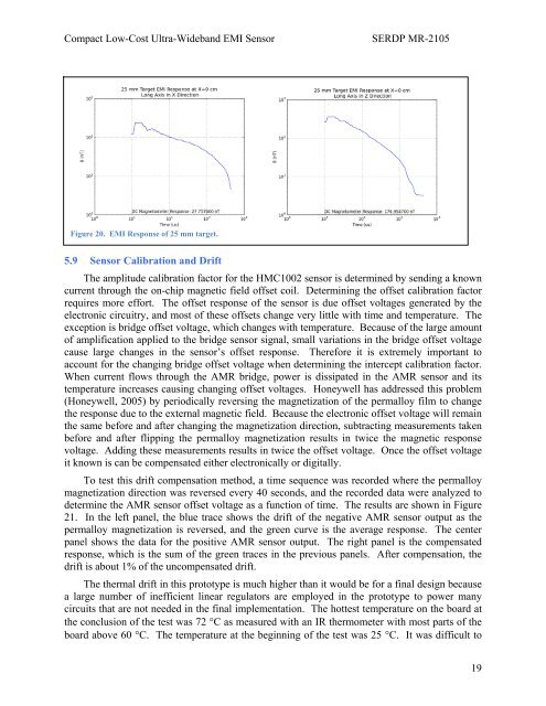
Compact Low-Cost Ultra-Wideb<strong>and</strong> EMI SensorSERDP MR-2105Figure 20. EMI Response of 25 mm target.5.9 Sensor Calibration <strong>and</strong> DriftThe amplitude calibration factor for the HMC1002 sensor is determined by sending a knowncurrent through the on-chip magnetic field offset coil. Determining the offset calibration factorrequires more effort. The offset response of the sensor is due offset voltages generated by theelectronic circuitry, <strong>and</strong> most of these offsets change very little with time <strong>and</strong> temperature. Theexception is bridge offset voltage, which changes with temperature. Because of the large amountof amplification applied to the bridge sensor signal, small variations in the bridge offset voltagecause large changes in the sensor’s offset response. Therefore it is extremely important toaccount for the changing bridge offset voltage when determining the intercept calibration factor.When current flows through the AMR bridge, power is dissipated in the AMR sensor <strong>and</strong> itstemperature increases causing changing offset voltages. Honeywell has addressed this problem(Honeywell, 2005) by periodically reversing the magnetization of the permalloy film to changethe response due to the external magnetic field. Because the electronic offset voltage will remainthe same before <strong>and</strong> after changing the magnetization direction, subtracting measurements takenbefore <strong>and</strong> after flipping the permalloy magnetization results in twice the magnetic responsevoltage. Adding these measurements results in twice the offset voltage. Once the offset voltageit known is can be compensated either electronically or digitally.To test this drift compensation method, a time sequence was recorded where the permalloymagnetization direction was reversed every 40 seconds, <strong>and</strong> the recorded data were analyzed todetermine the AMR sensor offset voltage as a function of time. The results are shown in Figure21. In the left panel, the blue trace shows the drift of the negative AMR sensor output as thepermalloy magnetization is reversed, <strong>and</strong> the green curve is the average response. The centerpanel shows the data for the positive AMR sensor output. The right panel is the compensatedresponse, which is the sum of the green traces in the previous panels. After compensation, thedrift is about 1% of the uncompensated drift.The thermal drift in this prototype is much higher than it would be for a final design becausea large number of inefficient linear regulators are employed in the prototype to power manycircuits that are not needed in the final implementation. The hottest temperature on the board atthe conclusion of the test was 72 C as measured with an IR thermometer with most parts of theboard above 60 C. The temperature at the beginning of the test was 25 C. It was difficult to19