

HD63265 Floppy Disk Controller Users Manual 2ed Mar89 - Bitsavers
HD63265 Floppy Disk Controller Users Manual 2ed Mar89 - Bitsavers
HD63265 Floppy Disk Controller Users Manual 2ed Mar89 - Bitsavers
- No tags were found...

Create successful ePaper yourself
Turn your PDF publications into a flip-book with our unique Google optimized e-Paper software.
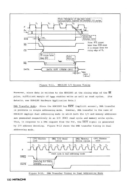
IOERDcsWR/1 ~ __________________________ -J(.!::..------,I CS comes later ILtEan B:~ __ J>,'4WRP~II'~HD64180 -lI Fetches Datal'----------'Note: WR comeslater than IOE sinceit is output from therising edge of T2DAT A--< DATA OUT (FROM CPU) r-tWDH( min)40n8Figure 9-11.HD64180 I/O Access TimingMoreover, since data is written to the <strong>HD63265</strong> at the rising edge of the WRpulse, sufficient margin of tWRP enables write as well as read cycles.details, see HD64180 Hardware Application Note.)(ForDMA Transfer Mode: Since the <strong>HD63265</strong> has DACK (implicit access), DMA transferis possible in single addressing mode. However, DMA transfer in the case ofHD64l80 employs dual addressing mode in which both the I/O and memory addressesare generated respectively in an I/O (FDC) read cycle and memory write cycle.Thus, in response to a DMA request from the FDC, the DACK signal is generatedby I/O address decoding. Figure 9-12 shows the DMA transfer timing in dualaddressing mode.CPU MachinecycleDMA I/O ReadcycleDMA MemoryWrite cycleCPU MachinecycleDMA cycle in dual addressing modeDACKFigure 9-12.DMA Transfer Timing in Dual Addressing Mode100 HITACHI


