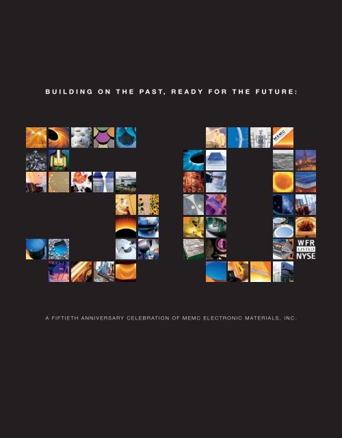
BUILDING ON THE PAST, READY FOR THE FUTURE: - MEMC
BUILDING ON THE PAST, READY FOR THE FUTURE: - MEMC
BUILDING ON THE PAST, READY FOR THE FUTURE: - MEMC

You also want an ePaper? Increase the reach of your titles
YUMPU automatically turns print PDFs into web optimized ePapers that Google loves.
B u i l d i n g o n t h e p a s t , r e a d y f o r t h e f u t u r e :<br />
a f i f t i e t h a n n i v e r s a r y c e l e b r at i o n o f m e m c e l e c t r o n i c m at e r i a l s , i n c .
B u i l d i n g o n t h e p a s t , r e a d y f o r t h e f u t u r e :<br />
a f i f t i e t h a n n i v e r s a r y c e l e b r at i o n o f m e m c e l e c t r o n i c m at e r i a l s , i n c .<br />
by Pat swinger<br />
edited and contributions by sheila o’connell
Copyright © 2009 by <strong>MEMC</strong><br />
All rights reserved, including the right to reproduce this work in<br />
any form whatsoever without permission in writing from the publisher,<br />
except for brief passages in connection with a review.<br />
For information, please write:<br />
The Donning Company Publishers<br />
184 Business Park Drive, Suite 206<br />
Virginia Beach, VA 23462<br />
Steve Mull, General Manager and Project Director<br />
Barbara Buchanan, Office Manager<br />
Pamela Koch, Senior Editor<br />
Tonya Hannink, Graphic Designer and Marketing Specialist<br />
Derek Eley, Imaging Artist<br />
Pamela Engelhard, Marketing Advisor<br />
Library of Congress Cataloging-in-Publication Data<br />
Swinger, Patricia, 1951–<br />
Building on the past, ready for the future : a fiftieth anniversary celebration of <strong>MEMC</strong> Electronic Materials, Inc. / by Pat Swinger ;<br />
edited and contributions by Sheila O’Connell.<br />
p. cm.<br />
Includes bibliographical references.<br />
ISBN 978-1-57864-574-9 (hbk. : alk. paper)<br />
1. <strong>MEMC</strong> Electronic Materials—History. 2. Semiconductor industry—United States—History. 3. Electronic industries—United<br />
States—History. 4. Electronics—Materials—United States—History. I. O’Connell, Sheila, 1968- II. Title.<br />
HD9696.S44M467 2009<br />
338.7’62138150973—dc22<br />
2009019379<br />
Printed in the United States of America at Walsworth Publishing Company
T A B L E O F C O N T E N T S<br />
Acknowledgments 6<br />
Letter from President and Chief Executive Officer Ahmad Chatila 7<br />
Chapter One The Birth of Technology 8<br />
Chapter Two <strong>MEMC</strong>’s Pioneering Years 14<br />
Chapter Three A Second Generation of Technology 26<br />
Chapter Four Great Strides in Technology 38<br />
Chapter Five A Global Company 50<br />
Chapter Six Strictly Business 64<br />
Chapter Seven Equations for Success 72
6<br />
A C K N O w L E D G M E N T S<br />
The editor acknowledges the following people as invaluable in helping design, write, and publish this<br />
book. Thank you for your time, effort, and belief in this project.<br />
Marsha Adkins<br />
Hidenor Aihara<br />
Linda Apprill<br />
Dr. KiMan Bae<br />
Albert Chen<br />
Peter Chen<br />
Karla Chaney<br />
Cheryl Collins<br />
Obata Design<br />
Steve Edens<br />
Dr. Henry Erk<br />
Dr. Robert Falster<br />
Dr. Graham Fisher<br />
Jerry Good<br />
Sherry Hagan<br />
Kazi Heinink<br />
Brenda Hubbartt<br />
Dr. Carissima Hudson<br />
Angela Jason<br />
John Kauffmann<br />
Dr. Bruce Kellerman<br />
Donna Kemm<br />
Brad Kohn<br />
Dr. Harold Korb<br />
Dr. DongMyun Lee<br />
Frank McLaughlin<br />
Joy Messner<br />
Bill Michalek<br />
Alice Muschany<br />
Roland Muschany<br />
Stanley T. Myers<br />
Sandra Prater<br />
Kay Sachs<br />
Dr. Robert Sandfort<br />
Mike Seacrist<br />
Dr. Larry Shive<br />
Roland Vandamme<br />
Dr. Robert walsh<br />
Brenda wilbourne<br />
Brian Zeig
F R O M P R E S I D E N T A N D C E O<br />
Ahmad Chatila<br />
From its modest beginnings as a small part of a division of a chemical company in Missouri to its position<br />
today as a major global enterprise, <strong>MEMC</strong> can look back on a long history of success.<br />
When we broke ground on our first facility to produce wafers for the semiconductor industry in 1959, no one<br />
could have predicted that the market for silicon wafers would be greater than 45 billion square inch units a<br />
year across two industries. Over the next 50 years <strong>MEMC</strong> technology would be at the heart of breakthroughs<br />
that helped shape our modern society. Silicon, and the silicon wafer products that <strong>MEMC</strong> manufactures,<br />
has enabled the modern integrated circuit which enables better healthcare, better communications, and<br />
even better entertainment. It has also advanced the burgeoning solar energy industry, by enabling us to<br />
efficiently harness clean renewable energy in effort to make solar power a more cost effective alternative to<br />
fossil fuels based energy systems. For <strong>MEMC</strong> this is just the beginning of the journey.<br />
Today, just as 50 years ago, research, development and innovation at <strong>MEMC</strong> are geared to solving our<br />
customers wafer needs of the day, including providing wafer solutions to improve their cost position<br />
and product offerings. <strong>MEMC</strong> currently holds more than 600 worldwide patents on silicon products and<br />
processes, plus more than 300 worldwide patent applications currently on file. Our focus on research and<br />
development in every area of silicon, and our long-standing tradition of quality have culminated in a<br />
company that is better positioned than at any point in our history to meet the demands of the highly<br />
competitive electronics and solar industries.<br />
The sacrifice and the true dedication of thousands of employees have enabled <strong>MEMC</strong> to survive and thrive<br />
for 50 years, a rarity in technology companies. We are eternally indebted to them. We are proud of our<br />
history, and our innovations, and we know we can achieve so much more. <strong>MEMC</strong> is only 50, and we know<br />
that what we have built will continue to grow. At the same time, our vision for the future encompasses<br />
more than silicon wafers for the semiconductor and solar industries. <strong>MEMC</strong> teammates are constantly<br />
seeking out new high growth opportunities, industries and sectors where we can utilize our solid R&D<br />
base and expand, both locally, and globally.<br />
I am honored to be leading <strong>MEMC</strong> in this critical time of our history. The technology made possible<br />
through the production of silicon wafers has revolutionized forever how we create, disseminate, retrieve<br />
and store information and how we generate energy. The people of <strong>MEMC</strong>, and the products we develop<br />
and manufacture, have made that possible. We are proud of our success over the past 50 years, and look<br />
forward to an equally successful future.<br />
Sincerely,<br />
Ahmad R. Chatila<br />
President and CEO<br />
<strong>MEMC</strong> Electronic Materials, Inc.<br />
7
8<br />
This is the story about a large corporation that, once<br />
upon a time, started as a small company and grew into<br />
a global force that helps make technology possible.<br />
From its inception, the company that is today <strong>MEMC</strong><br />
Electronic Materials, Inc., was a driving force in the<br />
technology that brought<br />
us the Information Age.<br />
At no other time in<br />
human history has the<br />
way we work, the way<br />
we play, and the way<br />
we communicate with<br />
each other changed as<br />
rapidly as it has in the<br />
period from 1970 to<br />
the present. Though<br />
the experiments and<br />
inventions of Thomas<br />
Edison in the late 1800s are considered the birth of<br />
the electronic age, it was the continuing research that<br />
took place in the first half of the twentieth century<br />
that laid the foundation for the Information Age.<br />
C H A P T E R O N E<br />
The Birth of Technology<br />
DiD yoU knoW?<br />
On February 6, 1959, a patent<br />
application was filed for a “Solid<br />
Circuit made of Germanium.”<br />
Subsequently, Texas Instruments was<br />
issued U.S. patent number 3,138,743<br />
for “Miniaturized electronic circuits.”<br />
In 2000 the importance of the<br />
Integrated Circuit (IC) was recognized<br />
when Jack Kilby was awarded the<br />
Nobel Prize in physics.<br />
When World War II ended in 1945, technology<br />
largely remained in the hands of universities, the<br />
military, and industry. Postwar life in America was<br />
good—relieved of the scarcities of war and full of<br />
promise. But even then, homes were still heated<br />
largely by coal, which<br />
was delivered by truck<br />
and dumped through a<br />
chute to the basement.<br />
Food was stored in an<br />
icebox, literally, in an<br />
insulated cabinet cooled<br />
by a block of ice. Clothes<br />
were laundered using a<br />
wringer washing machine<br />
and then hung on the<br />
line to dry. If you were<br />
lucky enough to have<br />
a telephone, your call<br />
was connected by a switchboard operator and<br />
subject to eavesdropping by all the other homes<br />
that shared your “party line.” Most households<br />
had a radio, their only source for music, news,
and broadcast entertainment. For the rare family<br />
that owned a television, the few shows that came<br />
over the waves were black-and-white and were<br />
broadcast for only a few hours each day.<br />
the transIstor<br />
This model was<br />
constructed to<br />
demonstrate<br />
how the earliest<br />
transistors<br />
worked in 1947.<br />
The lack of technology began to change when a<br />
research team consisting of John Bardeen, Walter<br />
Brattain, and William Shockley assembled at<br />
Bell Laboratories to find a replacement for the<br />
bulky and inefficient vacuum tube that Ambrose<br />
Fleming developed in 1904. On June 30, 1948, Bell<br />
Laboratories unveiled the transistor, which was<br />
smaller, more efficient, more reliable, and cheaper<br />
than the vacuum tube. Bardeen and Brattain<br />
received a patent for their invention in 1951, and<br />
the trio won the 1956 Physics Nobel Prize.<br />
Integrated CIrCuIts<br />
By 1956, transistors were commonplace, being used<br />
in everything from radios to the earliest computers.<br />
However, the entire electronics industry was<br />
looking for a way to overcome the “tyranny of<br />
numbers,” a phrase used to describe the dilemma<br />
that arose from the rising number of wires required<br />
to perform increasingly complex functions. In the<br />
late 1950s, two men, Jack Kilby at Texas Instruments<br />
and Robert Noyce at Fairchild Semiconductor,<br />
were working simultaneously but independently<br />
to overcome this challenge; their inventions would<br />
herald the start of a changing world.<br />
TrAveling AT The SPeeD<br />
of eleCTroniCS<br />
Thomas Ray, former St. Peters’ manager<br />
of Quality Assurance from 1981 to 1994,<br />
offered the following comparison of the<br />
transportation and electronics industry,<br />
taken from a very early training program<br />
used at the St. Peters plant.<br />
“If transportation (going back to the horse<br />
and buggy days) had advanced as fast as<br />
electronics over the past twenty years,<br />
the results would be truly astonishing. A<br />
Bell Laboratory scientist has calculated<br />
that, with equivalent advancements,<br />
your car might travel at one-quarter<br />
million miles an hour, get several hundred<br />
thousand miles per gallon of fuel, and be<br />
cheaper to throw away than to park at the<br />
airport overnight.”<br />
The Birth of Technology 9
10<br />
The first integrated circuit. Both men are credited with the invention of “the<br />
chip,” the monolithic (meaning formed from a<br />
single crystal) integrated circuit. While Jack Kilby<br />
1959 One wafer, one chip.<br />
1969 A dime-sized area of silicon held<br />
almost 10,000 transistors.<br />
1985 A dime-sized area of silicon held<br />
several hundred thousand<br />
transistors.<br />
1990s Millions of transistors resided on<br />
a silicon chip.<br />
2001 Circuitry on silicon can be<br />
shrunk to 0.13 microns—1/800th<br />
the width of a human hair—and<br />
the fastest chips operate at more<br />
than two billion calculations per<br />
second!<br />
successfully used germanium as the semiconductor<br />
in his model, it was Robert Noyce’s silicon version,<br />
and the fabrication techniques he devised, that<br />
made the integrated circuit practical. Both Texas<br />
Instruments and Fairchild Semiconductor filed for<br />
patents in 1959, and a legal battle ensued that lasted<br />
for over a decade. Patent No. 3,138,743 was issued to<br />
Jack Kilby and Texas Instruments for miniaturized<br />
electronic circuits in 1964. Patent No. 2,981,877<br />
was granted to Robert Noyce for the silicon-based<br />
integrated circuit. Eventually, Texas Instruments<br />
and Fairchild Semiconductor agreed to cross-license<br />
their technologies. Integrated circuits (ICs) gave<br />
device manufacturers the ability to integrate large
numbers of transistors, performing multiple<br />
functions, in a small area. The “chips” were<br />
mass-produced, using a photolithographic<br />
process, making them much cheaper and<br />
more reliable than the transistors that were<br />
constructed one at a time.<br />
early sIlICon ProduCtIon<br />
Prior to 1960, the standard for<br />
microelectronics manufacturing was<br />
referred to as “grown junction”<br />
production technology. This meant that<br />
the semiconductor device was actually<br />
grown as a part of the process of<br />
producing single crystal silicon. This enduse<br />
device growth is why companies like<br />
Westinghouse, IBM, and Siemens were<br />
among the earliest silicon producers. The<br />
development of planar semiconductor<br />
device technology and the development<br />
of a reproducible Czochralski silicon<br />
production process essentially divorced<br />
the device technology from the silicon<br />
industry. Dr. Ramo Pelling, manager<br />
of the first commercial semiconductor-<br />
Dr. wallene Derby, head of the Dayton, Ohio, research lab,<br />
which later relocated to St. Louis, Missouri.<br />
Bardeen, Brattain, and Shockley (seated) on the cover of<br />
electronics magazine September 1948 “Crystal Triode” issue.<br />
grade silicon production facility at DuPont and<br />
later the first president of Monsanto Silicon,<br />
observed, “As the industry started to grow in<br />
the 1960s, companies like Monsanto with their<br />
chemical materials background caught up to the<br />
semiconductor manufacturers quickly (in terms of<br />
technology).”<br />
MeMC’s Monsanto roots<br />
<strong>MEMC</strong> Electronic Materials, Inc., originated as part<br />
of the Inorganic Chemical Division of the Monsanto<br />
Chemical Corporation. Founded in 1901 by John<br />
F. Queeny, Monsanto started out manufacturing<br />
the artificial sweetener, saccharin. Over the years,<br />
The Birth of Technology 11
12<br />
Float Zone reactors for polysilicon<br />
production at Merano, 1962.<br />
Montecatini’s Merano plant began<br />
experimental production of silicon as<br />
early as 1958.<br />
The Novara plant in the 1970s. Montecatini<br />
merged with Edison in 1964 to become<br />
Montedison. Montedison then established a<br />
new company, SMIEL, in 1974, which built<br />
the plant in Novara in 1976 for its wafering<br />
operations. In 1980, both the Merano and<br />
Novara plants became part of Dynamit<br />
Nobel Silicon.<br />
Single crystal production at the Merano<br />
plant, 1962. Montecatini went through<br />
several transformations, eventually being<br />
acquired by Dynamit Nobel in 1980,<br />
the company that would later become<br />
an integral part of <strong>MEMC</strong> Electronic<br />
Materials, Inc.
Moore’S lAW<br />
Monsanto grew and<br />
acquired other companies.<br />
One of particular note was<br />
the Thomas & Hochwalt<br />
Laboratories in Dayton, Ohio, which<br />
Monsanto purchased in 1936. It was<br />
in Dayton that several of <strong>MEMC</strong>’s<br />
pioneers, Drs. Robert Walsh and<br />
Wallene Derby among them, got their<br />
start performing research on gallium<br />
arsenide for the manufacture of light<br />
emitting diodes (LED). Eventually, the<br />
Dayton lab relocated to Monsanto’s<br />
world headquarters in St. Louis,<br />
Missouri.<br />
In 1959, Monsanto broke ground at<br />
the St. Peters plant site cementing its<br />
commitment to the silicon wafer industry.<br />
The developments in silicon technology<br />
that took place at the St. Peters plant in the<br />
coming years would form the foundation<br />
for a technological explosion that continues<br />
to this day.<br />
Sources:<br />
http://www.pbs.org/transistor/album1/index.html<br />
http://www.xnumber.com/xnumber/kilby.htm<br />
http://www.computerhistory.org<br />
www.semi.org/en/P043595<br />
Gordon Moore, for whom Moore’s Law is named, started his career at Shockley Labs in 1956<br />
and went on to co-found Fairchild Semiconductor in 1957 and Intel Corporation in 1968. widely<br />
known for his 1965 prediction that the number of transistors on a computer chip would double<br />
approximately every year, he refers to this prediction as “a wild extrapolation of very little<br />
data.” Though his original prediction was only for the ensuing ten-year period, he reviewed it<br />
in 1975 and, based on technological advancements at that time, adjusted it to doubling every<br />
twenty-four months and extended it for another ten years. Asked about the future durability of<br />
Moore’s Law, he said, “We’re getting pretty close to molecular dimensions in the devices we’re<br />
making now, and that’s going to become a fundamental limit in how we can continue to shrink<br />
things. So, it’s going to change after another two or three process generations—I don’t know<br />
exactly when.”<br />
The Birth of Technology 13
14<br />
DiD yoU knoW?<br />
The Czochralski process takes its name<br />
from Jan Czochralski, a Polish scientist<br />
who discovered this method for pulling<br />
crystal rods as early as 1916. It is said<br />
he discovered the Czochralski method<br />
in 1916 when he accidentally dipped<br />
his pen into a crucible of molten tin<br />
rather than his inkwell. He immediately<br />
pulled his pen out to discover that<br />
a thin thread of solidified metal was<br />
hanging from the nib. The nib was<br />
replaced by a capillary, and Czochralski<br />
verified that the crystallized metal was<br />
a single crystal.<br />
st. Peters, MIssourI<br />
When Monsanto Chemical Company broke ground<br />
for the St. Peters plant in 1959, it was the newest<br />
addition to their Inorganic Chemicals Division.<br />
C H A P T E R T w O<br />
<strong>MEMC</strong>’s Pioneering Years<br />
The plant was to manufacture “ultra-pure silicon<br />
metal, a material used in the manufacture of<br />
transistors and rectifiers,” according to J. L.<br />
Christian, the division’s general manager. This<br />
new venture was the culmination of several<br />
years of research conducted at Monsanto’s two<br />
research labs (St. Louis and Dayton, Ohio) and<br />
represented Monsanto’s first major step toward<br />
supplying products for the emerging electronics<br />
industry. St. Peters, approximately thirty<br />
miles west of St. Louis, Missouri, was a small<br />
rural village in 1959, and the clean air of the<br />
countryside was considered ideal for the extreme<br />
degree of cleanliness required for silicon wafer<br />
production.<br />
The people who stood at the groundbreaking in<br />
St. Peters could not imagine the range and scope<br />
of the products that would one day be possible as<br />
a result of the work accomplished at this plant and<br />
at <strong>MEMC</strong> plants around the world. Few people<br />
can provide a better perspective than Stanley<br />
T. Myers, president and CEO of Semiconductor
1959 press release.<br />
Equipment and Materials International (SEMI),<br />
who worked at the St. Peters plant during its early<br />
years. In an interview he gave as part of SEMI’s<br />
oral history project, Mr. Myers respectfully refers<br />
to the pioneering engineers at St. Peters as “a<br />
bunch of cowboys” and recalls that the first crystalgrowing<br />
equipment was all “hand-grown,” for<br />
the first ten years or so. Sounding just a little<br />
astonished at his own recollections, he said, “My<br />
first crystal-growing piece of equipment was a<br />
converted drill press, if you can imagine. The<br />
chamber was made up of a quartz inner tube, and<br />
then an outer tube was Pyrex. We circulated water<br />
between the quartz and the Pyrex to remove the<br />
heat, and the crystal was inside the quartz tube.<br />
You wouldn’t do that today for anything because<br />
it would blow up on you if you got a crack in<br />
the glass. If the water hit the crystal, it wasn’t a<br />
pretty picture.” Luckily,<br />
he reports, though it<br />
did happen a few times,<br />
no one was injured.<br />
Compared to the extreme<br />
safety measures in place<br />
today at <strong>MEMC</strong>, it is<br />
difficult to imagine taking<br />
such risks. However,<br />
risk taking is a quality<br />
inherent in pioneers,<br />
and pioneers they were.<br />
<strong>MEMC</strong> produced its<br />
first three-quarter-inch<br />
(19mm) silicon wafer in<br />
February 1960.<br />
Polysilicon was produced<br />
using the Siemens-<br />
Westinghouse process<br />
for which Monsanto had<br />
purchased a license. Dr.<br />
Henry W. Gutsche, who<br />
Dr. Stanley T. Myers takes a<br />
well-deserved breather.<br />
<strong>MEMC</strong>’s Pioneering Years 15
1959<br />
August 6, J. L.<br />
Christian, vice<br />
president of Monsanto<br />
Chemical Company,<br />
issues a press<br />
releasing announcing<br />
construction of a<br />
new plant for the<br />
manufacture of ultrapure<br />
silicon metal in<br />
St. Charles County,<br />
Missouri.<br />
1961<br />
Montecatini (Italian<br />
chemical company)<br />
undertakes the<br />
strategy to develop<br />
a pilot production of<br />
poly and single crystal<br />
at Merano. This Italian<br />
company would later<br />
become part of <strong>MEMC</strong>.<br />
1962<br />
Dr. Robert walsh of<br />
<strong>MEMC</strong> pioneers the<br />
chemical mechanical<br />
polishing process.<br />
1965<br />
Initially, Gordon Moore<br />
observes that transistor<br />
density is doubling every<br />
12 months. It is later<br />
modified to 24 months.<br />
The term ”Moore’s law“<br />
was coined around 1970<br />
by Caltech professor,<br />
VLSI pioneer, and<br />
entrepreneur Carver<br />
Mead.<br />
1966<br />
Scientists at <strong>MEMC</strong><br />
begin developing zerodislocation<br />
crystal.<br />
1968<br />
The first computer with<br />
16 integrated circuits is<br />
manufactured.<br />
The Czochralski (CZ)<br />
crystal-growing process is<br />
put into manufacturing at<br />
<strong>MEMC</strong>.<br />
Chemical mechanical<br />
polishing of silicon wafers<br />
is established at <strong>MEMC</strong>.<br />
joined the Monsanto Electronics Division<br />
in 1964, developed the process that helped<br />
make <strong>MEMC</strong> successful during his earlier<br />
years at Siemens.<br />
FloatIng Zone (FZ) Crystals<br />
The earliest crystals were grown using<br />
the Floating Zone (FZ) method and were<br />
used in the production of power rectifiers<br />
and transistors. Dr. Graham Fisher, current<br />
director of Intellectual Property for <strong>MEMC</strong>,<br />
described the process: “It started out with<br />
a polysilicon rod, and the process involved<br />
creating a molten zone with a moveable<br />
heater. The molten zone (floating zone or<br />
liquid zone) was thin and was held in place<br />
by surface tension. The floating zone could<br />
be moved slowly down the rod allowing<br />
single crystal silicon to grow behind it, thus<br />
converting polysilicon structure to single<br />
crystal. This could be repeated multiple<br />
times and the crystal would then be very<br />
pure, but it was very expensive to do. The<br />
crystals were quite small; the wafers were<br />
approximately half a millimeter thick, and<br />
you’d typically produce about twenty-five<br />
to thirty wafers to an inch.”<br />
By 1979, Monsanto St. Peters was supplying<br />
approximately 80 percent of the U.S. market<br />
for float-zoned silicon. The float zone<br />
process was phased out in the mid-1980s<br />
in favor of another process for producing<br />
crystal that had finally matured—the<br />
Czochralski (CZ) method.<br />
the CZoChralskI Method<br />
Growing crystals for wafers<br />
was job one at <strong>MEMC</strong>.<br />
However, the growing<br />
of crystals often meant<br />
more capacity, and<br />
Early CZ crystal.<br />
more space was needed,<br />
so the plants would
Aerial view of St. Peters plant, 1960.<br />
also have to grow. As early as 1962, the original<br />
plant building was expanded to provide for the<br />
Czochralski method of making single crystal<br />
rods. A Polish scientist named Jan Czochralski<br />
invented the technique in the early 1900s.<br />
Credited for discovering this method of pulling<br />
metallic monocrystals, he is still recognized as one<br />
of the founding fathers of today’s semiconductor<br />
technology despite the fact that his research<br />
underwent considerable scrutiny in politically<br />
torn World War II Europe. In the late 1950s, the<br />
process was revisited as a possible method of<br />
producing silicon for transistor production and<br />
was widely adopted during the 1960s.<br />
The Czochralski method made much larger<br />
diameter wafers possible even though it had<br />
one disadvantage. Oxygen from the crucible,<br />
in which the silicon was melted, contaminated<br />
PioneerS AnD CoWboyS<br />
when you consider how crude some of<br />
the early processes of silicon production<br />
appear compared to those of today, it’s<br />
not surprising that words like “pioneer”<br />
and “cowboy” come to the minds of those<br />
who were there at the time. Some of what<br />
they experienced in those early years truly<br />
was heroic, and some of it has its comedic<br />
side. Consider, for instance, how the<br />
first wafers were shipped. While millions<br />
of dollars would eventually be spent<br />
developing packaging that kept the wafers<br />
clean and chip-free, Don westhoff recalled<br />
that the original FZ polished wafers were<br />
shipped to a customer (probably GE) in a<br />
coin-wrapping package.<br />
<strong>MEMC</strong>’s Pioneering Years 17
18<br />
in hiS oWn WorDS: Dr. roberT WAlSh<br />
on CheMiCAl MeChAniCAl PoliShing<br />
“When we started out, there was no<br />
integrated circuit industry. All the wafers that<br />
Monsanto was selling were just lapped wafers<br />
or etched wafers that went into devices—one<br />
wafer, one device. They were trying to make<br />
these multiple circuits on a wafer and the<br />
photographic process they used required very<br />
flat surfaces. You can’t get that with etching<br />
alone. They needed the wafers to be nicely<br />
polished, and then epi grown on the surface.<br />
The normal polishing techniques used very<br />
fine abrasives but no matter how fine an<br />
abrasive you use, you damage the surface<br />
of the crystal. You couldn’t see them in the<br />
substrate, but when they grew the layer,<br />
they’d show up. Growing an epi layer is a<br />
very serious test of how good a surface you<br />
have. we couldn’t get satisfactory yields and<br />
surfaces with the old polishing method. we<br />
had to come up with something new.<br />
“The early machines were optical polishing<br />
machines. what we found was (we were<br />
running with the finest aluminum oxide you<br />
could buy), that if you kept polishing with<br />
that same suspension of aluminum oxide, if<br />
you kept going, eventually you’d get much<br />
better surfaces on the wafers. At first we<br />
attributed it to wearing down the particle<br />
size even further until it was fine enough.<br />
Then I realized that what it really was, was<br />
that we were adding silicon to the polishing<br />
solution. These machines would fling the<br />
polishing solution off the edge and it would<br />
go down and be pumped back up so we<br />
were actually adding silicon to the polishing<br />
solution. So, thinking about all that, I<br />
thought, ‘Monsanto makes a product that’s a<br />
colloidal silicon.’ So we tried it one day and<br />
it just worked like a charm. It was in water,<br />
too, but it was alkaline. we needed it to be<br />
alkaline to keep it in suspension. The minute<br />
we hit that, the epi yields went up. And as<br />
Dr. Robert walsh developed the chemical-mechanical<br />
process for polishing wafers and received a North<br />
America SEMI Award for his work in 1986.<br />
soon as we saw that all the scratches went<br />
away on the epi surface, we knew we had<br />
something. Basically, that polishing process is<br />
what made integrated circuits possible.”<br />
when asked how it felt to be such a wellknown<br />
pioneer in the silicon wafer industry,<br />
Bob modestly replies, “Well, it’s nice,”<br />
though he received the SEMI Award of North<br />
America in 1986, an award established in<br />
1979 “to recognize outstanding technical<br />
achievement and meritorious contribution” to<br />
the industry. He recalls those early years as<br />
“the fun years,” saying, “It seemed like every<br />
day there was a new challenge to tackle.”
Small epitaxial wafer.<br />
the crystal. This<br />
posed a problem<br />
for wafers made<br />
for rectifiers. However, when the process of<br />
gettering was developed, the oxygen was used to<br />
attract impurities such as iron, copper, and nickel<br />
away from the surface of the wafer, making CZgrown<br />
crystals preferable for semiconductors.<br />
Monsanto’s work in this area in the 1980s led<br />
by Drs. Korb, Craven, and others was very<br />
significant. Later work done by Dr. Robert Falster<br />
and his team, trademarked in the mid-1990s as<br />
“Magic Denuded Zone,” cemented <strong>MEMC</strong>’s long<br />
history of controlling oxygen behavior in silicon.<br />
1 st<br />
MeMC “FIrsts”<br />
As <strong>MEMC</strong> marks its fiftieth year of silicon wafer<br />
production, the people of <strong>MEMC</strong> are extremely<br />
proud of the “Firsts” this company can claim.<br />
Though you will find these “Firsts” scattered<br />
throughout <strong>MEMC</strong>’s history, some of the most<br />
significant discoveries are attributed to the<br />
people who pioneered silicon wafer production<br />
at St. Peters.<br />
CheMICal MeChanICal PolIshIng<br />
One of the most notable innovations during this<br />
time remains an industry standard—the process<br />
of chemical mechanical polishing developed by<br />
Dr. Robert Walsh.<br />
Men operate BD-2 zone refiners, 1964.<br />
Polishing, October 1970.<br />
<strong>MEMC</strong>’s Pioneering Years 19
20<br />
Dr. Robert Sandfort, who was named president and chief operating officer of <strong>MEMC</strong> Electronic<br />
Materials, Inc., in 1989, recalled a few colleagues during those pioneering years at St. Peters.<br />
“Monsanto had a first-class technical operation and was able to accommodate itself to all kinds<br />
of personalities just to get the expertise that<br />
came with it.” Among those brilliant, standout<br />
personalities was a man named Dr. Henry Gutsche.<br />
Dr. Gutsche joined Siemens in 1954 as a research<br />
chemist at their laboratories in Pretzfeld,<br />
Germany. In 1956, Siemens received a patent<br />
for the work Dr. Gutsche did to produce the first<br />
semiconductor grade silicon which was 1000 ohm<br />
cm P-type uncompensated Si single crystal. In<br />
1964, after a few years with Merck, Dr. Gutsche<br />
joined Monsanto Electronics Division in Research<br />
and Development and continued his pattern of<br />
outstanding achievements. Dr. Sandfort fondly<br />
recalled the slouch hat that Dr. Gutsche wore tilted<br />
off to one side and remembers him as being “quite<br />
a character—a very sentimental man,” a trait that<br />
Dr. Sandfort attributes to the time Dr. Gutsche and<br />
his wife spent in a Nazi prison camp during world<br />
war II. In 1979, Dr. Gutsche received a SEMI award<br />
for his outstanding contributions to silicon wafer<br />
Dr. Henry Gutsche was responsible for setting up<br />
the Siemens process at St. Peters.<br />
Up until 1965, Monsanto St. Peters produced<br />
and sold unpolished wafers for discrete devices<br />
like silicon-controlled rectifiers. With the<br />
development of integrated circuits, the device<br />
manufacturers required a more perfect wafer<br />
surface.<br />
From 1960 to 1965, Dr. Robert Walsh worked at<br />
Monsanto’s St. Louis research center developing a<br />
process to make epitaxial (epi) wafers after having<br />
spent several years in Dayton, Ohio, developing a<br />
process for single crystal gallium arsenide for III-<br />
V semiconductors. When he came to St. Peters,<br />
Dr. Walsh took on the task of devising a polishing<br />
process that would provide a more perfect wafer<br />
surface for growing epi layers.<br />
reCAlling Dr. gUTSChe<br />
technology. Eccentric—perhaps; a brilliant pioneer—<br />
most certainly.<br />
At the time, wafers were 1” in diameter and 152<br />
microns thick with a tolerance of 19 microns.<br />
The very fine abrasives used for polishing the<br />
wafers created scratches in the surface. Though<br />
they weren’t visible in the substrate, they<br />
appeared once the epi layer was grown. The<br />
ultimate solution that Dr. Walsh devised was<br />
the chemical-mechanical method of polishing<br />
with colloidal silica in which the mechanical<br />
component was used to maintain the flatness of<br />
the wafer, and the chemical component kept the<br />
surface damage-free. The process of chemicalmechanical<br />
polishing is a key enabling factor for<br />
production of integrated circuits.
Up to this point, Dr. Walsh<br />
recalled, Monsanto hadn’t shown<br />
any interest in selling polished<br />
wafers. “Everybody was trying<br />
to make perfect surfaces. When<br />
IBM got our wafers, they became<br />
very interested because they<br />
had their own internal material<br />
department and they couldn’t<br />
make those perfect surfaces,” he<br />
recalled. In fact, IBM managed to<br />
purchase the license for chemicalmechanical<br />
polishing, trading<br />
some patents with Monsanto as<br />
part of the deal. Within the next<br />
couple of years, sales of polished<br />
wafers greatly increased.<br />
ePItaxIal layers<br />
By 1964, 1” wafers went<br />
into commercial production<br />
at St. Peters and shortly<br />
thereafter were replaced by<br />
1.5” wafers. Then, in 1966,<br />
the first epi reactors were<br />
built and installed, giving<br />
<strong>MEMC</strong> the ability to produce<br />
a wafer with a superior<br />
surface. In epi, a thin layer<br />
of silicon is grown on top of<br />
the polished slice surface by<br />
heating it to a temperature of<br />
approximately 2000 degrees<br />
Fahrenheit (approximately<br />
1100 Celsius) in a quartz<br />
chamber filled with hydrogen gas. Another gas<br />
containing silicon in combination with chlorine<br />
and hydrogen is introduced into the quartz<br />
chamber. The silicon layer grown in this manner<br />
is more perfect than the polished slice, having<br />
fewer defects and fewer impurities.<br />
The ability to produce wafers with an epitaxial layer<br />
Silicon brochure.<br />
increased in significance as device manufacturers<br />
required increasingly cleaner and flatter surfaces.<br />
Dr. Graham Fisher described the development<br />
of epi as “a platform improvement” saying, “In<br />
about 1984, <strong>MEMC</strong> was the first to commercialize<br />
epitaxial layers for CMOS technology. In its<br />
<strong>MEMC</strong>’s Pioneering Years 21
22<br />
Distillation columns at the St. Peters expansion, 1970.<br />
way, it was an enabling development to come<br />
up with that. People had been putting epitaxial<br />
layers on silicon for a while; what we did was<br />
commercialize it as a blanket layer.” The epi<br />
layer and the developed <strong>MEMC</strong> methods gained<br />
industry acceptance in the early 1980s as led by<br />
Dr. Jon Rossi and his <strong>MEMC</strong> teammates.<br />
Zero-dIsloCatIon Crystals<br />
In 1966, <strong>MEMC</strong> began developing zerodislocation<br />
crystals when their best customer at<br />
the time, IBM, advised Dr. Horst Kramer and<br />
his team that ingots and wafers showing slip<br />
patterns would no longer be acceptable. Slip<br />
patterns are essentially stress patterns that arise<br />
during the process of cooling the crystal, and the<br />
term “dislocation” refers to atoms that are out of<br />
place in the crystal lattice. Impurities, especially<br />
metals, can collect along the structural defects,<br />
deteriorating the performance of the device.<br />
Dr. Horst Kramer began his career in silicon<br />
crystal growth in 1959 at a company called Knapic<br />
Electro-Physics in Mountain View, California.<br />
By the mid-1960s, Dr. Kramer was given the<br />
task of eliminating slip from pulled crystals. Dr.<br />
Kramer’s notes record the discovery:<br />
The first experiments showed pretty much what we<br />
expected: an increase in pull rate resulted in a more<br />
concave interface; all other parameters remaining the<br />
same, different seed and crucible rotation combinations<br />
could change the interface from convex to concave.<br />
The next parameter was the melt level, i.e., the height<br />
of the crucible above the melt. In order to save silicon<br />
and time, I decided to skip growing the initial melt and<br />
start with only half the charge of silicon. The moment<br />
we were finished with the neck and started to increase<br />
the crystal diameter, we knew we had something<br />
special on our hands. The secondary growth lines in<br />
the taper were absolutely flat, and reflected light like a<br />
perfect mirror. The primary growth lines were strongly<br />
ridged and uniform, with no skips. In the body of the<br />
crystal, the primaries became flat, and the secondaries<br />
were visible only as shadowy lines. The bottom of the<br />
crystal, growing in the shape of an upside-down taper,<br />
also had pronounced flats, although here they occurred<br />
on the primaries. The flats sparkled like the faces of a<br />
diamond! We had just grown the first faceted silicon<br />
crystal!
Dr. Horst G. Kramer.<br />
As Dr. Kramer noted in his report, his discovery<br />
of “Zero-Dislocation” crystal growth “made<br />
the growth of large-diameter crystals possible,”<br />
saying that he did “not believe that even a<br />
150mm diameter crystal having a low dislocation<br />
density could be grown.” Further, he explained,<br />
“Dislocations are such large crystal defects that<br />
they could not be tolerated in today’s [1966]<br />
device fabrication.”<br />
PuttIng down roots<br />
Despite having garnered 80 percent of the market<br />
share by the time <strong>MEMC</strong> opened its doors,<br />
Left is Dr. Bobby D. Stone, who invented St. Peters’ zone-refining equipment, BD-1, BD-2, and BD-3.<br />
<strong>MEMC</strong>’s Pioneering Years 23
24<br />
business got off to a slow start. Nonetheless,<br />
the 1960s remained a period of steady growth<br />
for the company and laid the foundation for<br />
<strong>MEMC</strong>’s future reputation as a leader in the<br />
industry. In sharp contrast to its rural setting<br />
and the cornfields that surrounded the St. Peters<br />
plant, researchers there were giving birth to a<br />
technological boom. Monsanto’s roots in research<br />
and development helped create an environment<br />
that bred technological innovations, a trait<br />
that remains a hallmark of <strong>MEMC</strong> Electronic<br />
Materials, Inc., to this day.<br />
Additional Sources:<br />
www.semi.org<br />
www.semi.org/en/About/Awards/index.htm<br />
http://www.eoearth.org/article/Czochralski_Jan<br />
wafer evaluation, early 1980s.<br />
Flattening and grinding wafers, 1970.
Left is Dr. Forrest “Frosty” Williams, resident expert in III-V’s. George McLeod was head of Monsanto’s electronics business. In<br />
the early 1970s, he made the trail-breaking move to go offshore.<br />
Aerial view of St. Peters plant, 1970.<br />
<strong>MEMC</strong>’s Pioneering Years 25
26<br />
C H A P T E R T H R E E<br />
A Second Generation of Technology<br />
By 1970, consumer electronics were becoming a<br />
growth industry, most visibly in entertainmentrelated<br />
products. The first home video games, played<br />
through television receivers, hit the market in 1972.<br />
In 1975, CB radios were all the rage along with the<br />
“Pong” home video game. The 1980s saw the first<br />
personal computers and<br />
videocassette recorders<br />
coming into the market,<br />
and by 1988, CDs were<br />
more popular than vinyl<br />
records among music<br />
enthusiasts.<br />
The 1970s and 1980s were<br />
a time of tremendous<br />
growth in the silicon wafer<br />
industry interrupted by<br />
head-spinning highs and<br />
lows. In hindsight, the downturns that occurred in<br />
the mid-1970s and again in the mid-1980s did so for a<br />
variety of reasons. Over-production caused, in part,<br />
by optimistic chip manufacturers, competition from<br />
DiD yoU knoW?<br />
A man named Ray Tomlinson<br />
developed the first electronic mail<br />
system in 1971. The first message<br />
of any substance was a message<br />
announcing the availability of network<br />
email and gave instructions to use the<br />
‘at’ sign to separate the user’s name<br />
from the host computer name.<br />
the emerging Japanese market, and, of course, the<br />
constant drive toward advancements in technology,<br />
all contributed to the turbulence of these two<br />
decades. Monsanto St. Peters responded to these<br />
challenges by focusing on technological excellence<br />
combined with constant quality improvement, a<br />
strategy that has brought<br />
the company to where it is<br />
today.<br />
In a study of the fiftyyear<br />
history of the<br />
semiconductor silicon<br />
industry, Steven Walsh<br />
and others concluded<br />
that success in the silicon<br />
industry is determined<br />
by a company’s ability<br />
to maintain the highest<br />
standards of industry-specific technological<br />
competence. He writes, “By 1980, materials<br />
companies had overtaken both captive and<br />
fabrication and assembly-based producers, and
Monsanto advertisement, featuring Hubert Dohmen, Tom Ray,<br />
Andy Taylor, and Jerry Gayer.<br />
U.S.-based merchant chemical suppliers dominated<br />
the single crystal silicon as well as polysilicon<br />
markets. Monsanto was the leading silicon supplier<br />
in the world and dominated the worldwide single<br />
crystal silicon production with facilities in the U.S.,<br />
Europe and Asia.” According to Walsh, the silicon<br />
manufacturers most likely to succeed were those<br />
who excelled at both disruptive and evolutionary<br />
technology. Disruptive technologies were those<br />
innovations that remained proprietary and<br />
therefore captive for a period of time; evolutionary<br />
technologies referred to the constant incremental<br />
improvements on existing processes. Monsanto St.<br />
Peters, with its strong background in research and<br />
development, was ideally suited for both.<br />
ICs at the wheel<br />
By the early 1970s, integrated circuit technology<br />
was largely driving the silicon wafer business.<br />
Stanley Myers was Monsanto’s Silicon Business<br />
Group director in 1972. He recalled, “In the early<br />
1960s we knew [the development of the integrated<br />
circuit] would have a significant impact, not only on<br />
growing the crystal, but also polishing the wafer—<br />
slicing, polishing, and modifying the crystal and<br />
putting the epi layers on the wafer. All of these<br />
things became much more prominent as soon as IC<br />
SeMi<br />
Semiconductor Equipment and Materials<br />
Institute (SEMI) was formed in 1970 to<br />
provide visibility and support to the<br />
equipment and materials manufacturers<br />
that were the backbone of the burgeoning<br />
electronics industry. Having increased<br />
marketplace awareness through its<br />
expositions, SEMI worked to establish<br />
their standards program through which<br />
they continue to foster open markets,<br />
constructive competition, and cost<br />
containment throughout the semiconductor<br />
industry. In 1979, they established the<br />
SEMI award, given each year to individuals<br />
for outstanding technical achievements.<br />
when the industry reached global status<br />
in the mid-1980s, SEMI redefined itself to<br />
stay in step. The “I” in SEMI was changed<br />
from “Institute” to “International.”<br />
SEMI offers its members technical<br />
conferences, educational events, and<br />
market data collection and analysis<br />
and advocates for the industry in public<br />
policy, environmental, health and safety<br />
issues, workforce development, and<br />
investor relations. With eleven offices in<br />
manufacturing regions around the world,<br />
SEMI serves the manufacturing supply<br />
chains for the microelectronic, display, and<br />
photovoltaic industries.<br />
A Second Generation of Technology 27
28<br />
1970<br />
The SEMI organization<br />
is founded by Bill<br />
Hugle, Fred Kulicke,<br />
and John Dannelly.<br />
1971<br />
Electronic mail<br />
(E-mail) is invented.<br />
1972<br />
The word<br />
processor<br />
is invented.<br />
1973<br />
Three-inch wafers<br />
go into commercial<br />
production at the St.<br />
Peters plant.<br />
1975<br />
Four-inch wafers<br />
go into commercial<br />
production at the St.<br />
Peters plant.<br />
1976<br />
Montedison builds a<br />
second plant in Novara,<br />
Italy. This plant would<br />
later become merged<br />
with <strong>MEMC</strong>.<br />
1979<br />
<strong>MEMC</strong> is the first to<br />
commercially produce<br />
125mm wafers.<br />
<strong>MEMC</strong> builds a plant in<br />
Kuala Lumpur, Malaysia.<br />
The computer floppy disc is<br />
invented.<br />
The microprocessor is<br />
invented. It is considered a<br />
computer on a chip.<br />
<strong>MEMC</strong> opens Kuala Lumpur,<br />
Malaysia, plant.<br />
<strong>MEMC</strong> is the first wafer<br />
supplier to control oxygen.<br />
The inaugural SEMI Awards<br />
are held, with eleven<br />
individuals recognized<br />
for their achievement in<br />
advancing equipment and<br />
materials technology.<br />
applications took hold and the market began<br />
to develop.”<br />
Industry experts agree that device<br />
manufacturers drove the change toward<br />
larger wafers, primarily as a means for<br />
cutting costs. Circuits were printed on<br />
the wafers using photolithography, and,<br />
simply put, the more devices per wafer,<br />
the lower the cost. But they also agree that<br />
the silicon wafer manufacturers, including<br />
<strong>MEMC</strong>, complied with the demands in part<br />
as a means of asserting their technological<br />
capabilities. <strong>MEMC</strong>’s customers in the fastmoving<br />
electronics industry were putting<br />
more and more circuitry on smaller chip<br />
areas. To do that, they needed smaller line<br />
widths, which called for flatter, cleaner silicon<br />
wafers with improved physical and electrical<br />
characteristics.<br />
The increased wafer diameters that resulted<br />
in lower costs for the device manufacturers<br />
came at quite a price for the silicon wafer<br />
suppliers, <strong>MEMC</strong> among them. Each increase<br />
in wafer diameter meant an outlay of capital<br />
for the equipment required to produce<br />
that larger wafer, as well as increased costs<br />
incurred to achieve the tighter specifications<br />
that were inherent in every diameter increase.<br />
As with their customers, cost cutting became a<br />
priority for the silicon wafer manufacturers.<br />
MovIng overseas<br />
The St. Peters plant was expanded in 1962,<br />
1967, 1970, and again in 1974, by which<br />
time the plant had doubled from its original<br />
capacity. By the early 1970s, competition<br />
from the Japanese silicon manufacturers was<br />
getting everyone’s attention. Stan Myers<br />
recalls that in the mid-1970s Japan’s silicon<br />
production was “probably two generations<br />
behind the U.S.,” but that “they were on a<br />
very, very rapid learning curve.”
Kuala Lumpur plant in Malaysia.<br />
<strong>MEMC</strong>’s move toward international status was<br />
prompted by competition from the Japanese. The<br />
manufacturing site in Kuala Lumpur, Malaysia,<br />
built in 1970, was <strong>MEMC</strong>’s first location in the<br />
Asian semiconductor market. The Kuala Lumpur<br />
site was chosen because of its proximity to the<br />
largely English-speaking population of Singapore<br />
and because Malaysia’s free industrial trade zone<br />
provided attractive tax incentives for foreign<br />
investors. The most significant benefit, however,<br />
was the savings that resulted from lower costs<br />
on everything from the physical plant to supplies<br />
to labor. The St. Peters plant grew 2.25” crystals,<br />
shipped them to the Kuala Lumpur plant for slicing<br />
and polishing, and then on to customers.<br />
iii-vS<br />
In the 1970s, the St. Peters plant started<br />
manufacturing the III-V compounds used to<br />
make light-emitting diodes, those red and<br />
green lights that first showed up in pocket<br />
calculators and digital wristwatches. This<br />
operation was eventually dismantled and<br />
sold to General Instruments in 1979.<br />
A Second Generation of Technology 29
30<br />
wafer lapping, 1975.<br />
The Milton Keynes plant in England opened<br />
operations in 1986. Etched wafers received from<br />
the United States were polished and cleaned for<br />
Monsanto’s European customers, among them<br />
well-known names like Siemens, SGS, Thompson<br />
CSF, Philips, Telefunken, National Semiconductor,<br />
and Motorola. The site included a research and<br />
development center and an applications research<br />
lab.<br />
sIZe Matters<br />
<strong>MEMC</strong>’s focus on providing customers with the<br />
cost-saving larger diameter wafers combined with<br />
the highest-quality features, led to their reputation<br />
as a leader in the silicon wafer industry during<br />
these turbulent years and beyond.<br />
In 1975, Monsanto St. Peters was the first to<br />
commercially produce 4” (100mm) wafers and again<br />
the first to commercially produce 125mm wafers in<br />
1979. The 150mm wafer was first produced in 1981,<br />
and at the time, a leading IC manufacturer projected<br />
a five-fold increase in chip yield when switching<br />
from 100mm to 150mm wafers. In addition, the<br />
flatness specification of the 150mm wafer varied<br />
A ChAnging MArkeT<br />
In the April 23, 1990, issue of the St. Louis<br />
Business Journal, Roger McDaniel summed<br />
up the Asian influence on the silicon wafer<br />
market: “In 1980, half of the silicon sold<br />
in the world was consumed in the United<br />
States and only 25 percent was consumed<br />
in Japan. By 1985, the numbers were<br />
reversed as Japan gained dominance in<br />
the semiconductor memory market. Now<br />
the Koreans and Taiwanese are challenging<br />
the Japanese, and the United States and<br />
Europe are fighting to stay in the race.”<br />
less than two microns within a 20mm field of view.<br />
In 1984, <strong>MEMC</strong> partnered with IBM to produce the<br />
200mm wafer.<br />
evolvIng teChnology<br />
In 1975, <strong>MEMC</strong> became the first wafer supplier<br />
to control oxygen in a growing crystal, a process<br />
that simply wasn’t crucial in the early days. Dr.<br />
Graham Fisher explains the significance of the<br />
process: “Because the crucible is made of quartz,<br />
which is silicon dioxide, in the process of growing<br />
silicon, oxygen from the crucible can contaminate<br />
the crystal. In the early days, the level of oxygen<br />
wasn’t very important. As time went on, customers<br />
started using more complex processes for making<br />
integrated circuits during which the wafer is heated<br />
and cooled multiple times. During the manufacture<br />
of integrated circuits, the successive heating and<br />
cooling causes the supersaturated oxygen atoms<br />
to precipitate in the form of small oxide clusters.<br />
The higher the oxygen concentration the higher the<br />
level of precipitation, so control of oxygen became<br />
an important development.”<br />
Ironically, solving one problem created another<br />
problem in its place because the low oxygen wafers<br />
were not as strong mechanically. Graham recalls
Monsanto’s <strong>MEMC</strong> tradeshow booth.<br />
the time spent in the early 1980s trying to get the<br />
right balance of oxygen and understanding how<br />
the wafer would behave in a customer’s device<br />
line. “We were trying to get the oxygen at just the<br />
right level so when the customer would process<br />
the wafer on the fab line, the oxygen would start<br />
to precipitate but only to a certain degree and<br />
not near the wafer surface,” he explains. “This<br />
way you maintain the mechanical strength, but<br />
the precipitates form in the bulk and not near the<br />
surface where the device is formed. An even bigger<br />
advantage of this distributed precipitation behavior<br />
is that the precipitates trap any unwanted metal<br />
impurities that might diffuse into the wafer in the<br />
bulk region away from the active device<br />
region at the surface. The technique is<br />
known as ‘intrinsic gettering.’”<br />
About the same time, <strong>MEMC</strong> added<br />
edge grinding to the basic wafer process.<br />
Starting with the 100mm wafers, <strong>MEMC</strong> began<br />
grinding the edges to a rounded profile. Before this<br />
step was added, the crisp, squared edge of the wafer<br />
was more susceptible to chipping. Ground edges<br />
meant less waste, and therefore reduced costs, for<br />
both <strong>MEMC</strong> and their customers.<br />
100mm wafers and ingot.<br />
A Second Generation of Technology 31
32<br />
Zone refiner.<br />
1 st<br />
Left to right: Dr. Dave Keune, Dr. Bob Craven, and Dr. Harold<br />
Korb in the Applications Research laboratory, 1975.<br />
oZonated de-IonIZed<br />
water For waFer CleanIng<br />
In 1983, <strong>MEMC</strong> achieved three very significant<br />
“firsts” in the area of silicon wafer cleaning with<br />
ozone. They were the first to use ozone in a silicon<br />
wafer cleaning process, first to use the combination<br />
of HF and ozone in a silicon wafer cleaning<br />
sequence, and the first to design and install cleaning<br />
equipment capable of performing an ozone cleaning<br />
process step for silicon wafers.<br />
These innovations were driven by <strong>MEMC</strong>’s<br />
recognition that the traditional cleaning chemistries,<br />
referred to as Standard Cleans 1 & 2, could not<br />
achieve the surface metals levels that were going<br />
to be required by the industry, given the purity of<br />
cleaning chemicals available. At that time, <strong>MEMC</strong><br />
was simultaneously developing new methods for<br />
surface aluminum analysis that supported the<br />
work in cleaning. When surface metals, especially<br />
aluminum, were too high, the customer observed<br />
non-uniform oxide growth rates as a result.
Employees wear Clean<br />
Silicon Group t-shirts<br />
that were part of an<br />
advertising campaign<br />
to establish Monsanto’s<br />
wafers among the<br />
cleanest on the market.<br />
Rack cleaner.<br />
Ingot slicing.<br />
A Second Generation of Technology 33
34<br />
SPArTAnbUrg<br />
leArning DiSCovery<br />
In 1980, <strong>MEMC</strong> built a plant in Spartanburg,<br />
South Carolina, and began commercial<br />
production of 6” (150mm) wafers.<br />
when production began, the plant had<br />
ten thousand square feet of space and<br />
forty-five employees. Combined with<br />
the Malaysia plant and expansions at<br />
St. Peters, Spartanburg brought <strong>MEMC</strong>’s<br />
total manufacturing capacity to 330<br />
million square inches per year, a 400<br />
percent increase over that of 1978. John<br />
Kauffmann, currently senior vice president<br />
of worldwide Sales, Customer Service,<br />
and Marketing, started his career with<br />
Monsanto at the Spartanburg plant and<br />
recalls that there was a worldwide learning<br />
process that took place between plants.<br />
“At our plant we made an etched wafer so<br />
it wasn’t a completely finished product and<br />
we were shipping it to our plant in Japan.<br />
At that time, I was a technology leader and<br />
these wafers that we thought were really,<br />
really good opened up a learning exchange<br />
between how we did things in Spartanburg<br />
and how things were done in Japan.” It<br />
was such an all-encompassing learning<br />
experience that it led to a task force,<br />
which John spearheaded, to help improve<br />
the quality of the product coming out of<br />
the United States.<br />
Dr. Larry Shive,<br />
<strong>MEMC</strong> Senior<br />
Fellow, commented,<br />
“This work was<br />
far ahead of<br />
any previous or<br />
subsequent cleaning<br />
and was truly<br />
r e v o l u t i o n a r y. ”<br />
The process was<br />
developed by Wilbur<br />
Krusell and coworkers<br />
in 1982 and<br />
was first installed<br />
in St. Peters as the<br />
ozone rack cleaner<br />
Dr. Larry Shive.<br />
in 1983. It was then copied at <strong>MEMC</strong> factories<br />
around the world. Ozone cleaning technology is<br />
now a key cleaning step in every wafer and device<br />
factory in the world, giving device manufacturers a<br />
predictable and uniform oxide growth rate.<br />
MultIstrate sIlICon waFers<br />
A 1984 brochure entitled “Monsanto: Technology<br />
in Silicon” touts the advantages of their MultiStrate<br />
silicon wafers, a new class of multilayer products.<br />
By this time, device manufacturers were building<br />
thousands of ICs on a single chip, requiring<br />
improved circuit performance and yield. As a<br />
result, the electronic circuitry interacted more<br />
dynamically with the physical properties of the<br />
silicon. As the brochure said, “the cutting edge<br />
of semiconductor technology is now within the<br />
silicon.”<br />
MultiStrate silicon wafers were a new class<br />
of integrated silicon substrate products. The<br />
MultiStrate product line was a family of new<br />
epitaxial wafers for applications involving<br />
high-density silicon-gate CMOS and NMOS.<br />
Trademarked EpiStrate, this series of products<br />
John Kauffmann, senior vice president of worldwide Sales,<br />
Customer Service, and Marketing.
Inner diameter saw with back grinding capability, which<br />
reduced the amount of required lapping.<br />
combined the superior flatness of the basic<br />
Czochralski wafer with an epitaxial layer grown<br />
on the polished surface. With the MultiStrate<br />
product line, substrate characteristics could<br />
STC horizontal saw, late 1970s.<br />
be matched to the epitaxial process using a<br />
Monsanto proprietary technique for engineering<br />
the epitaxial/substrate interface to enhance largescale<br />
circuit performance and yield.<br />
wafers are inserted into and extracted from a warming oven, slowly allowing them to heat or cool to avoid dislocations in the<br />
crystal lattice.<br />
A Second Generation of Technology 35
36<br />
Mortin Sentman slicing wafers.<br />
Polishing two-inch wafers.<br />
aPPlICatIon-sPeCIFIC waFers<br />
The introduction of the MultiStrate product line<br />
perhaps marked the beginning of the applicationspecific<br />
approach to increasing customer demands.<br />
In the late 1970s and early 1980s, Monsanto<br />
was instrumental in SEMI’s efforts toward<br />
standardization of silicon wafer production.<br />
This was important, primarily because the more<br />
standardization Monsanto could incorporate<br />
into its manufacturing process, the easier and<br />
more cost effective it was to accommodate the<br />
customers’ requests for specific features as device<br />
manufacturers required increasing customization.
The highly competitive nature of the consumer<br />
electronics products industry created a cost<br />
consciousness that trickled down to the silicon<br />
wafer industry. The challenge for the wafer<br />
manufacturers was to accommodate the<br />
device manufacturers’ demands for increased<br />
customization while simultaneously maintaining<br />
their own cost competitiveness. Perhaps the key<br />
to <strong>MEMC</strong>’s survival and success was its good<br />
fortune at being birthed by a large company with<br />
the deep pockets required to stay on the cutting<br />
edge of a technology that everyone believed would<br />
someday pay off. When <strong>MEMC</strong> was featured<br />
in the September 1990 issue of the St. Charles<br />
County Business Network, the article read, “Since<br />
the early 1960s the giant silicon company has had<br />
to keep up with an extremely demanding and<br />
competitive market where [companies] who fail to<br />
keep up with advanced technology are out of the<br />
ballgame in short order.” Nearly twenty years later,<br />
<strong>MEMC</strong>’s vast technological experience and highly<br />
competitive business model has, in turn, made it<br />
extremely difficult for new competitors to enter the<br />
market.<br />
Additional sources:<br />
“The semiconductor silicon industry roadmap: Epochs drive<br />
by the dynamics between disruptive technologies and core<br />
competencies,” Steven T. walsh et al., Elsevier, Inc., 2003.<br />
www.semi.org<br />
http://openmap.bbn.com/~tomlinso/ray/firstemailframe.<br />
html<br />
<strong>MEMC</strong>’s plant in Spartanburg,<br />
South Carolina, was built in 1979–80.<br />
A Second Generation of Technology 37
38<br />
In 1980, with the basic technology of silicon<br />
wafers firmly established and the sophistication<br />
of integrated circuits increasing rapidly, the very<br />
nature of the silicon wafer industry changed.<br />
From 1950 to 1980, progress in the semiconductor<br />
industry was driven<br />
primarily by materials<br />
science. That shifted in<br />
1980 as process sciences<br />
began to dominate<br />
silicon wafer production<br />
as customers began to<br />
demand application-<br />
specific wafers.<br />
In response, <strong>MEMC</strong><br />
amplified its focus on quality, technological<br />
innovation, and customer satisfaction. Application<br />
engineers were assigned to customers to better<br />
understand their silicon wafer needs. At times,<br />
the customers’ processes were modeled inhouse<br />
to ensure the performance of <strong>MEMC</strong>’s<br />
products in the customer’s wafer fabrication<br />
C H A P T E R F O U R<br />
Great Strides in Technology<br />
DiD yoU knoW?<br />
In silicon wafer manufacturing,<br />
an impurity level of one part per<br />
billion equates to one foot in the<br />
distance to the moon.<br />
lines. Simultaneously, <strong>MEMC</strong>’s key strategy was<br />
to constantly improve its own manufacturing<br />
efficiency to maintain its technological superiority<br />
and cost competitiveness.<br />
1 st<br />
granular<br />
PolysIlICon<br />
In 1991, <strong>MEMC</strong>’s Pasadena<br />
facility was the first<br />
company in the industry<br />
to develop a process using<br />
granular polysilicon. In<br />
the original chunk<br />
polysilicon process<br />
obtained from Siemens,<br />
rods of polysilicon were produced by the<br />
decomposition of an ultra-pure gas containing<br />
silicon, hydrogen, and chlorine. The rods were<br />
crushed into manageable chunks, which were<br />
then placed into the CZ puller crucible by hand.<br />
Silicon is relatively hard, and the crushing process<br />
posed a purity problem since the hammers that
were used to crush the silicon also contaminated it.<br />
The chunks of polysilicon had to be hand-stacked<br />
by human beings; therefore, the CZ puller had to<br />
be at room temperature for charge stacking. After<br />
loading the crucible with charge, the CZ pull<br />
chamber was closed, purged and evacuated, bakedout<br />
and heated to melt the silicon.<br />
In the late 1980s a new polysilicon process to produce<br />
granular polysilicon was developed at what is now<br />
known as the <strong>MEMC</strong> Pasadena plant. This process<br />
produces beads of silicon, approximately 1mm to<br />
2mm in diameter, with the same or better level of<br />
purity. Having small beads of polysilicon eliminated<br />
the need for crushing and all the problems and<br />
extra steps that arose with it. The beads could be<br />
poured into the crucible like a liquid, which meant<br />
the crucible could be filled much more easily,<br />
automatically, and without the need for human<br />
contact and the risk of contamination that resulted.<br />
Also, the puller could be filled with polysilicon<br />
much faster, with the puller atmosphere purged<br />
and relatively hot, thus shortening the turn-around<br />
time for the puller and increasing its production<br />
capacity. Inspired by the container for Pringles potato chips, Monsanto<br />
invented the Flip Tran Cassette container in 1981 to ship wafers<br />
with dry nitrogen to ensure cleanliness. wafers were canned in<br />
a controlled atmosphere to keep the wafer surface pristine.<br />
Granular polysilicon is<br />
poured into a quartz<br />
crucible.<br />
<strong>MEMC</strong> ad touts the benefits of granular polysilicon.<br />
Great Strides in Technology 39
40<br />
1979<br />
Sony introduces the<br />
walkman.<br />
1981<br />
<strong>MEMC</strong> is the first to<br />
commercially produce<br />
150mm wafers.<br />
1982<br />
Technical center<br />
is introduced in<br />
Edogawa-ku, Tokyo.<br />
1983<br />
Programmer Jaron<br />
Lanier first coins the<br />
term “virtual reality.”<br />
1984<br />
<strong>MEMC</strong> is the first<br />
to commercialize<br />
200mm wafers in<br />
partnership with IBM.<br />
1985<br />
<strong>MEMC</strong> is the first<br />
wafer manufacturer<br />
to develop polysilicon<br />
gettering.<br />
<strong>MEMC</strong> begins construction<br />
on its Spartanburg, South<br />
Carolina, plant, which is<br />
completed in 1980.<br />
<strong>MEMC</strong> ships wafers in<br />
the “Flip-Tran” cassette.<br />
The “can” is sealed with<br />
dry nitrogen to ensure<br />
cleanliness.<br />
<strong>MEMC</strong> pioneers epi wafers<br />
for CMOS applications.<br />
Japan overtakes the U.S.<br />
as the world’s leading<br />
semiconductor producer.<br />
Microsoft invents windows<br />
program.<br />
Chunk polysilicon is melted.<br />
Granular polysilicon is melted.<br />
1 st<br />
PolysIlICon getterIng<br />
As semiconductor devices shrank in size,<br />
they became more susceptible to deleterious<br />
effects of metallic contamination present<br />
in the semiconductor-device-fabrication<br />
sequence. Besides degrading the performance<br />
of the device, trace metals can form surface<br />
silicides that ruin devices by disrupting the<br />
device fabrication steps such as etching and<br />
dopant diffusion.<br />
<strong>MEMC</strong> was the first to commercialize<br />
polysilicon gettering, a technique for trapping<br />
the minute quantities of metallic contaminants<br />
present in silicon device processing away<br />
from the areas where the devices are to be<br />
built. The technology, developed in 1985,<br />
involved both internal gettering and external<br />
gettering.
In external gettering, a fine-grain layer of<br />
polysilicon is grown on the backside of the wafer to<br />
draw impurities away from the critical regions of<br />
the wafer where devices are built. Wafers with this<br />
backside EG layer yield better and are less sensitive<br />
to process upsets that might ordinarily degrade or<br />
destroy devices. Monsanto (<strong>MEMC</strong>) was the first<br />
wafer manufacturer to offer external gettering, a<br />
process developed under the lead of Dr. Dale Hill.<br />
By the late 1980s, almost 50 percent of all wafers<br />
made by Monsanto had the polysilicon gettering<br />
layer applied to them.<br />
Another external gettering process adopted by<br />
<strong>MEMC</strong> was called custom-designed gettering<br />
or CDG. Sandblasting of the wafer backside can<br />
create damage points at the back surface. These<br />
damage points would also effectively trap metallic<br />
impurities. By changing the sandblasting conditions<br />
A product brochure describing the benefits of<br />
granular polysilicon as produced at the <strong>MEMC</strong><br />
Pasadena plant.<br />
<strong>MEMC</strong> 300mm wafer.<br />
to control the density of damage points, a wide<br />
range of damage levels could be created in order to<br />
provide the correct gettering effect to optimize the<br />
customer’s device yields.<br />
<strong>MEMC</strong>’s process of internal gettering is featured in<br />
the November 2003 issue of Solid State Technology.<br />
Great Strides in Technology 41
42<br />
1986<br />
<strong>MEMC</strong> builds the<br />
Utsunomiya, Japan,<br />
plant—becomes the<br />
first non-Japanese<br />
wafer maker with<br />
manufacturing and<br />
research facilities in<br />
Japan.<br />
1987<br />
SEMI and the<br />
Semiconductor<br />
Equipment Association<br />
of Japan enter into<br />
an agreement to<br />
exchange market data<br />
on a monthly basis.<br />
1988<br />
Digital cellular phones<br />
invented.<br />
1989<br />
High-definition<br />
television invented.<br />
SEMI establishes the U.S.<br />
Japan Trader Partners<br />
Conference to ease<br />
trade friction between<br />
the U.S. and Japanese<br />
semiconductor industry.<br />
1 st<br />
<strong>MEMC</strong> Japanese teammates band together to build<br />
quality products for customers.<br />
utsunoMIya, JaPan<br />
In 1986, the opening of the Utsunomiya<br />
plant made <strong>MEMC</strong> the first non-Japanese<br />
wafer producer to have manufacturing<br />
and research facilities in Japan. Unlike the<br />
move to Kuala Lumpur, which was largely<br />
motivated by opportunities for cutting costs,<br />
the Utsunomiya plant reflected an emerging<br />
strategy for locating close to the customer.<br />
Among the Japanese customers, Nippon<br />
Electric Company (currently known as<br />
NEC) was the largest and, acknowledging<br />
Monsanto as a world leader in silicon wafer<br />
production, sought them out as a back-doorto-front-door<br />
supplier. A short-lived attempt<br />
at warehousing proved to have little benefit<br />
to <strong>MEMC</strong>; silicon wafers do not respond well<br />
to warehousing, and NEC’s specifications for<br />
wafers were constantly changing.<br />
Despite these early challenges, the 300mm<br />
Center of Excellence was added to the<br />
Utsunomiya plant in 1998, and it remains<br />
an integral part of <strong>MEMC</strong>’s presence in the<br />
Asian and Japanese markets.
MeMC JAPAn<br />
Originally built in 1986, the Utsunomiya<br />
plant is located approximately one hundred<br />
kilometers north of Tokyo where <strong>MEMC</strong> Japan<br />
is headquartered. In 1997, the Utsunomiya<br />
plant underwent a $250 million expansion for<br />
the production of 300mm wafers and currently<br />
produces 200mm and 300mm polished silicon<br />
wafers and 200mm and 300mm epitaxial<br />
wafers. with the support of the Tokyo sales<br />
office, the Utsunomiya plant is dedicated to<br />
the highly competitive and advanced Japanese<br />
and Asian markets.<br />
Utsunomiya is the capital and most populous city<br />
of Tochigi Prefecture, Japan. Historically speaking,<br />
the city is known for the Battle of Utsunomiya<br />
Castle, a battle between pro-Imperial and<br />
Tokugawa shogunate forces during the Boshin war<br />
in May 1868. Modern-day Utsunomiya, however, is<br />
renowned for its jazz and gyoza. The Utsunomiya, Japan, plant opened in 1986.<br />
1 st<br />
200MM waFers<br />
In 1984, <strong>MEMC</strong> became the first company to<br />
commercialize 200mm wafers, a feat achieved in<br />
partnership with IBM. As with every previous<br />
increase in diameter size, the demand for quality<br />
rose and specifications increased. In 1990, <strong>MEMC</strong><br />
announced the purchase of several million<br />
dollars worth of equipment used to make 200mm<br />
diameter wafers from IBM. Ralph Hartung, vice<br />
president for U.S. manufacturing at the time,<br />
called the 8” wafer “a whole new generation that<br />
is becoming a boom business.” The purchase<br />
of equipment from IBM allowed <strong>MEMC</strong> to<br />
supplement existing production capacity to help<br />
the company maintain its position in the silicon<br />
wafer market.<br />
200mm crystal production at St. Peters.<br />
Great Strides in Technology 43
44<br />
Ralph Hartung, vice president, US Manufacturing. Photo from<br />
the early 1980s.<br />
Liz Dulick leads a tour of post polishing through final cleaning<br />
at the St. Peters plant.<br />
An article in the October 1992 edition of<br />
Semiconductor International explained the<br />
significance of the 200mm diameter wafer to the<br />
semiconductor industry:<br />
Semiconductor manufacturers are gearing up to use<br />
200mm wafers primarily for high volume, large area<br />
circuits such as DRAMs, SRAMs, flash-EPROMs<br />
DrAM, SrAM, AnD eProM<br />
DRAM or Dynamic Random Access Memory<br />
is a type of random access memory that<br />
stores each bit of data in a separate<br />
capacitor within an integrated circuit.<br />
Random access means that locations in<br />
the memory can be written to or read<br />
from in any order, regardless of the<br />
memory location that was last accessed.<br />
SRAM or Static Random Access Memory<br />
is faster and less power hungry than<br />
DRAM. Owing to a more complex internal<br />
structure, SRAM is less dense than DRAM<br />
and is therefore not used for highcapacity,<br />
low-cost applications such as<br />
the main memory in personal computers.<br />
An EPROM, or Erasable Programmable<br />
Read-Only Memory, is a type of memory<br />
chip that retains its data when its power<br />
supply is switched off.<br />
and HDTV related memory. Officials at <strong>MEMC</strong><br />
Electronic Materials foresee, over the next five years,<br />
the sale of 200mm wafers will be increasing by 800<br />
percent.<br />
ContInued InnovatIons<br />
Up until 1992, the Inner Diameter Saw, or ID saw,<br />
was the standard operation for slicing wafers. For<br />
the production of 200mm wafers, the move was<br />
made toward wire sawing. With wire sawing, one<br />
complete ingot is placed in the saw, and a single<br />
helical wire makes multiple cuts through the ingot<br />
at the same time. Though much faster and more<br />
efficient than the ID saw, the potential downside is<br />
that if something goes wrong you risk losing the<br />
entire ingot. One advantage, however, is that while<br />
the diamond ID saw cut was about 350 microns<br />
wide, the wire saw is 200 microns wide, creating<br />
less waste per cut and more wafers per ingot.
Also notable is the fact that, during this time, the controls of<br />
the crystal-growing furnaces were changed to computer-digital<br />
systems, giving the operators finer gradations of control. It was<br />
one of those strange twists of fate where the silicon wafer <strong>MEMC</strong><br />
was making was improved through the use of the silicon-based<br />
circuits in the computerized control system.<br />
headlIne:<br />
“Monsanto to sell sIlICon waFer FIrM”<br />
Although the front-page article in the November 14, 1988,<br />
issue of Electronic News announcing Monsanto’s plans to sell<br />
its electronic products division didn’t exactly read like an<br />
obituary, for some it felt like one. As the nation’s sole producer<br />
of 8” silicon wafers, news of the impending sale sent shockwaves<br />
through Silicon Valley, and many feared it was an indication<br />
that the United States was losing its technological edge. Worse,<br />
the Department of Defense feared that the United States’ security<br />
could be jeopardized should silicon wafer production, a critical<br />
defense technology, leave the country.<br />
While some American companies,<br />
including IBM, Texas Instruments, and<br />
Motorola, had their own internal wafer<br />
production, none of these facilities was<br />
large enough to fill the gap should a<br />
crisis of national security occur. One<br />
Silicon Valley insider was quoted in<br />
Electronic News saying, “This is it. It’s<br />
all over. Monsanto was the last stand.”<br />
Headline announces Monsanto’s intent to<br />
sell <strong>MEMC</strong>.<br />
Above: wafer slicer, 2009.<br />
Below: This diagram explains both the inner diameter<br />
saw and wire sawing of wafers.<br />
Great Strides in Technology 45
46<br />
in the past several years, polysilicon has become an<br />
important and successful part of MeMC’s business,<br />
and Merano plays a big part in that success.
Though Monsanto’s electronics products division<br />
had long been a financial drain to the company, in<br />
a strange turn of events, it posted operating profits<br />
of $8 million for the first three quarters of 1988 on<br />
sales of $137 million. Monsanto had gone through a<br />
reorganization just three years prior, and since that<br />
time, speculation ran high that the company would<br />
renew its allegiance to chemicals, agriculture, and<br />
biotechnology products and exit the electronics<br />
materials business.<br />
An offer to purchase came from Hüls AG of<br />
West Germany, a subsidiary of VEBA AG. The<br />
previous year, Hüls announced its intention to<br />
purchase Dynamit Nobel Silicon (DNS), a large<br />
manufacturer of polyvinyl chloride as well as other<br />
petrochemicals, detergents, coatings, and specialty<br />
chemicals with sales of $1.9 billion in 1986 for<br />
primarily intermediate chemicals, among them<br />
trichlorosilane used to make polysilicon.<br />
Dr. Robert Sandfort recalled the concerns<br />
surrounding the sale to Hüls: “There were a lot of<br />
misgivings. Really, we would have preferred that<br />
Monsanto retain ownership of the company, but<br />
they did not want to do that. Monsanto was in the<br />
Novara, Italy, plant.<br />
DynAMiT nobel SiliCon<br />
position of concentrating its efforts on life sciences,<br />
biotechnology. So we saw that they were going to<br />
exit the business, and we thought, ‘There has to be<br />
somebody to buy it.’ We would have preferred that<br />
a U.S. company step forward and buy it, but they<br />
didn’t.”<br />
1957 A company named Montecatini begins research on silicon in Novara, Italy.<br />
1961 Montecatini constructs a pilot plant in Merano, Italy.<br />
1964 Montecatini merges with Edison. The new company is named Montedison.<br />
1974 Montedison establishes a new company, SMIEL, and begins wafer production in 1975.<br />
1976 SMIEL builds a new plant in Novara, Italy. Polysilicon and single crystal remains in<br />
Merano; the wafering operations are moved to Novara.<br />
1980 Dynamit Nobel acquires the silicon operation in Italy and Germany and changes its<br />
name to Dynamit Nobel Silicon.<br />
1983 DNS establishes a new technology center in Sunnyvale, California, USA.<br />
1984 DNS constructs a new wafer plant in Research Triangle Park, North Carolina. They ship<br />
their first lot of wafers in 1986.<br />
1987 DNS ships its first epi wafers out of Novara, Italy.<br />
1988 DNS’s silicon operation in Italy and Germany is acquired by Hüls (VEBA) and becomes<br />
DNS Electronic Materials.<br />
Great Strides in Technology 47
48<br />
Above: Epi reactor.<br />
Left: Epitaxial<br />
deposition.<br />
In December of 1988, the federal Committee on<br />
Foreign Investment in the United States (CFIUS)<br />
announced its intention to review the sale under<br />
the provisions of the 1988 Omnibus Trade Act, a law<br />
that gave the president the right to block the sale<br />
of a United States business to a foreign company if<br />
national security was threatened by the sale. Again,<br />
Bob Sandfort was in the thick of things: “It [the sale]<br />
did raise a lot of concern in Washington, and we<br />
had to have a number of meetings there to try and<br />
eMPloyee reCeiveS PATenT<br />
The July 1988 newsletter read as follows:<br />
Art Ackermann, Engineering Specialist at<br />
St. Peters, has received a U.S. patent,<br />
which he shares with Peter Tremont,<br />
retired CED engineer. The two men<br />
perfected a type of ozone technology used<br />
to make ultra pure deionized (D.I.) water.<br />
This unique process was developed in 1983<br />
right here at our St. Peters Site. In this<br />
process, ozone is added to D.I. water to<br />
kill bacteria particles, which, if present,<br />
can cause defects by sticking to the wafer<br />
surface. The process has had a dramatic<br />
positive impact on our wafer quality and<br />
yield. As a result, all of the Monsanto<br />
wafer facilities now use this technology.<br />
In 1986 and 1987 Bob Craven, TSD<br />
Superintendent, and Art Ackermann<br />
marketed the ozone technology to<br />
Monsanto customers. At the end of<br />
1987 the technology was licensed to<br />
Arrowhead Industrial water Company for<br />
additional worldwide marketing. To date,<br />
direct sales, licensing and royalties have<br />
grossed over three million dollars for our<br />
company. The technology will not be sold<br />
to our silicon competitors. Rather, it is<br />
marketed to device manufacturers to<br />
improve their yield and competitiveness.<br />
we believe that all device manufacturers<br />
will eventually utilize the Monsanto ozone<br />
technology to improve quality and yields.<br />
The ozone process is another example of<br />
Monsanto’s leading edge technology!<br />
understand their concerns. What they didn’t seem<br />
to understand in Washington was that we weren’t<br />
the only people making silicon. The Japanese had<br />
two franchises, Shin-Etsu Chemical and Osaka<br />
Titanium (currently known as Sumco), and the<br />
Germans had two franchises, Wacker and DNS, so
Missouri Governor John Ashcroft with Roger McDaniel,<br />
first CEO of <strong>MEMC</strong> Electronic Materials, Inc., 1989.<br />
they really weren’t losing the technology<br />
because it was already there.”<br />
This was the first time the law was<br />
invoked, and despite concerns expressed<br />
by representatives of the departments of<br />
Commerce and Defense, the Committee<br />
on Foreign Investment in the United States<br />
(CFIUS) voted unanimously to support<br />
the sale. Two primary factors contributed to this<br />
decision. First, Hüls assured CFIUS that they were<br />
committed to keeping the silicon wafer business in<br />
the United States. Second was the announcement that<br />
the company would be managed by a combination<br />
of current executives as well as Hüls officials.<br />
On February 7, 1989, then-president George H. Bush<br />
announced that he had given his permission for the<br />
sale of Monsanto Electronic Materials Company<br />
to Hüls AG. The West German government had<br />
already granted approval for the sale. All that<br />
remained to finish negotiations was approval from<br />
the governments of Japan and Malaysia where<br />
Monsanto Electronic Materials Company had<br />
manufacturing sites. Within a couple months of<br />
President Bush’s approval, the sale was finalized.<br />
Shortly thereafter, Dongbu Industrial Company<br />
took full ownership of an earlier joint venture<br />
between themselves and Monsanto located in the<br />
Republic of Korea, named Korsil. Hüls, who already<br />
owned the DNS facilities in Merano and Novara,<br />
Italy, prudently closed down wafer-making plants<br />
in Research Triangle Park, North Carolina, and<br />
Milton Keynes, England, in May of 1989.<br />
The new company, <strong>MEMC</strong> Electronic Materials, Inc.,<br />
was now the second largest manufacturer of silicon<br />
wafers in the world. With Dr. Roger McDaniel<br />
named as president and CEO, <strong>MEMC</strong> launched an<br />
entirely new era in the company’s history.<br />
<strong>MEMC</strong> made plans to build a 20,000-square-foot<br />
addition to the St. Peters plant to house its new<br />
world headquarters. When then Missouri governor<br />
John Ashcroft visited the plant, he commented,<br />
“The combination of Monsanto and DNS makes<br />
<strong>MEMC</strong> a major player in the world market for this<br />
highly specialized product and makes Missouri a<br />
world leader in this business.”<br />
In the ensuing years following the sale to Hüls,<br />
<strong>MEMC</strong> entered into some strategic alliances<br />
and joint ventures, both in the United States and<br />
abroad, to enhance their position in the world<br />
silicon market.<br />
Sources:<br />
St. Louis Post Dispatch, May 2, 1990<br />
St. Louis Post Dispatch, June 25, 1990<br />
St. Louis Business Journal, April 23, 1990<br />
Semiconductor International, October 1992<br />
http://en.wikipedia.org/wiki/Utsunomiya<br />
Great Strides in Technology 49
50<br />
Within a year of its merger with Dynamit Nobel<br />
Silicon (DNS) in 1989, the St. Peters plant, now the<br />
World Headquarters of <strong>MEMC</strong> Electronic Materials,<br />
Inc., added twenty thousand square feet to its facility.<br />
Capital funding totaling nearly $40 million was<br />
approved for the manufacturing and research facility<br />
to ensure <strong>MEMC</strong>’s survival in the highly competitive<br />
silicon wafer business. Roger<br />
McDaniel, then president and<br />
CEO, reported that <strong>MEMC</strong><br />
had about 23 percent of the<br />
world market of $1.5 billion for<br />
silicon wafers and anticipated<br />
sales of $390 million in 1990,<br />
an increase of approximately<br />
$40 million over 1989 sales.<br />
By 1991, <strong>MEMC</strong>’s sales were<br />
well over $400 million, and by 1994, the St. Peters<br />
plant produced two thousand different wafer types,<br />
90 percent of which did not exist three years prior.<br />
In 1995, Industry Week magazine named <strong>MEMC</strong> St.<br />
Peters one of the ten best manufacturing plants in<br />
the United States.<br />
C H A P T E R F I V E<br />
A Global Company<br />
DiD yoU knoW?<br />
On Earth, silicon is the second<br />
most common element,<br />
exceeded only by oxygen.<br />
From the time of Hüls’ purchase of <strong>MEMC</strong> to the<br />
late 1990s, the company once again saw a surge of<br />
technological innovations and industry alliances.<br />
<strong>MEMC</strong>’s strategy for secure growth was to expand<br />
manufacturing capacity for advanced products,<br />
maintain technology leadership in the industry,<br />
and focus on strategic alliances with customers and<br />
peer companies throughout<br />
the industry.<br />
JoInt venture—korea<br />
In 1990, <strong>MEMC</strong> announced<br />
its plans to enter into a joint<br />
venture agreement with<br />
Pohang Iron and Steel Ltd.<br />
(POSCO) and Samsung<br />
Electronics Company Ltd. to open a plant in South<br />
Korea under the name Posco Hüls Co., Ltd. “We<br />
have more than half of the Korean market now,”<br />
Roger McDaniel said. “We need to protect that.<br />
Korea is going after Japan in a strong way in the<br />
making of memory chips. From the Korean point of
MeMC’S firST Ceo, roger MCDAniel<br />
In 1996, Roger McDaniel retired following a thirty-four-year career that took him from entry-level<br />
chemical engineer at a small plant in West Virginia to the chief executive officer of the secondlargest<br />
silicon wafer manufacturer in the world. Mr. McDaniel joined Monsanto’s silicon business as<br />
director of Facilities and Planning in 1980. In 1982, he became the first person with responsibility<br />
for the silicon wafer business outside the United States. when interviewed for the Summer 1996<br />
issue of <strong>MEMC</strong> Today, he recalled those years when the industry shifted to international status.<br />
“In 1982, our sales were around $100 million, and only around $20 million of that was from<br />
international sales. Today, our group sales for just one quarter are equal to the total sales for all<br />
of the first four years I was with the silicon business. And, 60 percent of it now comes from sales<br />
outside the United States.”<br />
when Monsanto sold its electronics products business to Hüls in<br />
1989, McDaniel was in charge of operations. with the formation<br />
of <strong>MEMC</strong> Electronic Materials Company, Inc., he was named<br />
president and CEO. Upon his retirement, he commented on the<br />
satisfaction he felt watching the company grow. He said, “This<br />
organization has a real sense of purpose today. we are good at<br />
what we do, and are improving every day.”<br />
view, they will have invested $1 billion in this effort, and they will<br />
not want to be dependent on a foreign source for their silicon.”<br />
To this day, many Koreans consider both Samsung and POSCO<br />
symbols of national pride, and their affiliation with <strong>MEMC</strong> was<br />
a boost to the company’s international standing. The goal was<br />
to put <strong>MEMC</strong> in a position to compete in any market that developed<br />
anywhere in the world with the exception of Soviet-block countries where<br />
U.S. restrictions still applied to the sale of high technology products.<br />
The manufacturing facility was built at Cheonan City in the<br />
south Chungcheong province of South Korea. By 1993,<br />
the plant was fully operational for the manufacture of<br />
polished wafers.<br />
In June of 1996, a conference was held in Tao Yuan,<br />
Taiwan, to discuss <strong>MEMC</strong>’s plans for addressing<br />
the growing Asian silicon wafer market, which<br />
had more than tripled in the preceding five<br />
years. At the time, it was forecast to account<br />
for more than a third of the worldwide<br />
300mm wafer.<br />
A Global Company 51
1990<br />
Tim Berners-Lee<br />
creates the world<br />
Wide Web/Internet<br />
protocol (HTTP)<br />
and www language<br />
(HTML).<br />
1991<br />
Eight-inch wafers go<br />
into production at<br />
<strong>MEMC</strong>’s joint venture<br />
in Cheonan, South<br />
Korea.<br />
1993<br />
The global<br />
semiconductor<br />
equipment market<br />
exceeds $10 billion in<br />
sales for the first time.<br />
1994<br />
<strong>MEMC</strong>’s joint venture,<br />
Taisil Electronic<br />
Materials, is located in<br />
Hsinchu, Taiwan.<br />
1995<br />
<strong>MEMC</strong> Southwest, a<br />
joint venture with<br />
Texas Instruments,<br />
is established in<br />
Sherman, Texas, to<br />
produce six-inch<br />
wafers.<br />
1996<br />
Stan Myers, former<br />
president and CEO<br />
of Siltec and one of<br />
<strong>MEMC</strong>’s “Pioneers,” is<br />
appointed president<br />
of SEMI.<br />
1997<br />
<strong>MEMC</strong> St. Peters<br />
begins commercial<br />
production of 300mm<br />
wafers.<br />
1999<br />
<strong>MEMC</strong> introduces<br />
three new products:<br />
52 Optia, Aegis, and MDZ.<br />
The Pentium processor<br />
is produced.<br />
<strong>MEMC</strong> trades on the New<br />
York Stock Exchange as an<br />
Initial Public Offering under<br />
the stock symbol “WFR.”<br />
<strong>MEMC</strong> secures base<br />
patents on Perfect<br />
Silicon–brand wafers.<br />
<strong>MEMC</strong> Taisil plant 300mm opening ceremony, Hsinchu,<br />
Taiwan.<br />
silicon market by the year 2000, and several<br />
expansions reflected those projections.<br />
The joint venture plant in Cheonan, Korea,<br />
completed an expansion that increased<br />
its capacity to more than three hundred<br />
thousand 200mm wafers per month.<br />
JoInt venture—taIwan<br />
In 1994, <strong>MEMC</strong> entered into a joint<br />
venture with China Steel Corporation,<br />
China Development Industrial Bank, and<br />
Chiao Tung Bank. The company formed<br />
as a result of this joint venture was named<br />
Taisil Electronic Materials Corporation.<br />
The manufacturing facility was located<br />
in Hsinchu, a medium-sized city located<br />
about an hour south of Taiwan’s capital city<br />
of Taipei. Referred to as Taiwan’s “Silicon<br />
Valley,” the Hsinchu location gave the Taisil<br />
plant back-door access to many of <strong>MEMC</strong>’s<br />
Taiwanese customers. Tommy L. Cadwell,<br />
<strong>MEMC</strong>’s president of Asian Operations at<br />
the time, said that investment in the plant<br />
was expected to exceed $150 million. Taisil<br />
was Taiwan’s first large-diameter advanced<br />
silicon wafer producer. Its capacity upon<br />
its opening was eighty-five thousand<br />
wafers per month, but expansions quickly<br />
brought its capacity to its peak volume of<br />
three hundred thousand 200mm wafers per<br />
month.
even by 1995<br />
STAnDArDS<br />
According to an article in the<br />
October 2, 1995, St. Louis Post<br />
Dispatch,<br />
At some stages (of silicon<br />
manufacturing), the air in the<br />
process line is five million times<br />
cleaner than the atmosphere in St.<br />
Louis.<br />
The circuitry on Intel Corporation’s<br />
Pentium chip is equal in complexity<br />
to a street map of the entire<br />
United States and fits on a surface<br />
about the size of a fingernail.<br />
That same year, 1994, <strong>MEMC</strong> also<br />
purchased a silicon wafer plant in Santa<br />
Clara, California. The facility, previously a<br />
subsidiary of Kawasaki Steel Corporation,<br />
produced 100mm and 150mm silicon<br />
wafers and employed about two hundred<br />
people. The plant, known as Kawatech,<br />
was purchased to increase arsenic crystal<br />
capacity.<br />
the IBM ConneCtIon<br />
IBM and <strong>MEMC</strong> share an interdependent<br />
history that dates back to the earliest days<br />
of the St. Peters plant. During the late<br />
1980s, the two companies worked together<br />
to launch 200mm wafers. This success was<br />
beneficial to both companies as it furthered<br />
the relationship, and on many occasions<br />
IBM would work with <strong>MEMC</strong> on special<br />
development projects, and <strong>MEMC</strong> could<br />
reap the benefits of the relationship both<br />
technologically and financially.<br />
Groundbreaking ceremony at Posco Hüls, <strong>MEMC</strong>’s joint venture in<br />
Cheonan, South Korea.<br />
The plant in Cheonan, South Korea—MKC.<br />
Taisil Electronic Materials plant in Hsinchu, Taiwan.<br />
A Global Company 53
54<br />
300mm double-sided polishing.<br />
“Silicon-on-Insulator,” a.k.a. SOI, wafers were originally<br />
manufactured by SiBond, LLC, a joint venture between <strong>MEMC</strong><br />
and IBM. These wafers were produced in 2007.<br />
PASADenA PlAnT<br />
1983 Ethyl completes $150M<br />
investment to develop granular<br />
polysilicon manufacturing process.<br />
1985 Ethyl completes $70M investment<br />
in granular polysilicon<br />
manufacturing process—PA21.<br />
1987 Ethyl completes startup of PA21<br />
after investing an additional $50M<br />
in the process.<br />
1994 Ethyl spins off chemical business<br />
into a separate publicly traded<br />
company, Albemarle. Polysilicon<br />
manufacturing is part of the new<br />
company.<br />
1995 Albemarle sells PA21 to <strong>MEMC</strong> for<br />
$58M.<br />
1998 <strong>MEMC</strong> completes investment in an<br />
additional silane production unit,<br />
PA22, raising capacity to 2,500<br />
metric tons per year.<br />
2007 <strong>MEMC</strong> completes investment in<br />
third silane production unit, PA23,<br />
raising total capacity to 6,000<br />
metric tons per year.<br />
2008 <strong>MEMC</strong> completes investment in<br />
fourth silane production unit,<br />
PA24; this investment combined<br />
with expansions in Merano raises<br />
total <strong>MEMC</strong> capacity to 8,000<br />
metric tons per year.<br />
In 1994, <strong>MEMC</strong> again partnered with IBM to form<br />
a new company called SiBond, LLC. The company,<br />
based at St. Peters, used technology developed by<br />
the IBM Research Division plus manufacturing<br />
and sales techniques developed by <strong>MEMC</strong> in the<br />
creation of a specialty technology called “siliconon-insulator”<br />
(SOI) technology to be used for<br />
memory devices containing more than one gigabit<br />
of data.<br />
The specialty wafer’s makeup is a sort of sandwich
<strong>MEMC</strong>’s Pasadena plant, 2007.<br />
with a layer of silicon dioxide serving as an insulator<br />
between layers of silicon, providing a substrate<br />
for microcircuits that operate on reduced power<br />
consumption. The quick response microcircuit<br />
worked well in advanced devices such as laptops<br />
or hand-held computers and portable telephones.<br />
SOI wafers are energy efficient and eliminated<br />
the need for heavy batteries previously required<br />
for portable devices. SOI technology is currently<br />
a major component of some high-speed network<br />
services and direct-link entertainment devices.<br />
JoInt venture—Pasadena, texas<br />
Back in 1984, <strong>MEMC</strong> entered into a joint venture<br />
agreement with Ethyl Corporation to develop<br />
a process for making granular polysilicon.<br />
Ethyl Corporation operated the pilot plant,<br />
located in Pasadena, Texas. Then in July of 1995,<br />
<strong>MEMC</strong> purchased the production facility from<br />
Albemarle, a company that Ethyl Corporation<br />
had spun off its specialty chemical business in<br />
years prior, and established <strong>MEMC</strong> Pasadena. The<br />
acquisition of the Albemarle facility in Pasadena<br />
shored up the security of <strong>MEMC</strong>’s supply for<br />
polysilicon. When polysilicon was in tight<br />
supply in the mid-1990s, <strong>MEMC</strong> was producing<br />
more than half of its polysilicon internally and<br />
was also able to purchase from Hüls some of the<br />
raw material needed to make chunk polysilicon.<br />
Strengthening the internal supply chain with<br />
granular polysilicon provided <strong>MEMC</strong> with “a<br />
A Global Company 55
56<br />
<strong>MEMC</strong> Southwest Groundbreaking Ceremony, October 2, 1995.<br />
Left to right: Ron Backschies, human resources manager; J. R.<br />
Moore, finance manager; C. B. Lee, QA manager; Bob Bennett,<br />
100mm manager; Jerry Smith, engineering; Bob McCarley,<br />
150mm manager; David Eaton, customer service manager; Frank<br />
McLaughlin, 200mm manager; David Fronterhouse, 150mm<br />
manager; Mike Grimes, 150mm operations manager; John<br />
Robinson, president and COO, <strong>MEMC</strong> Southwest.<br />
Aerial view of <strong>MEMC</strong> Southwest, Sherman, Texas, in December<br />
1996.<br />
Crystal puller, first tool installed at <strong>MEMC</strong> Southwest, November<br />
1996.<br />
good secret weapon.” Located ten miles<br />
southeast of downtown Houston, Texas,<br />
<strong>MEMC</strong> Pasadena continues to produce<br />
ultra-pure granular polysilicon, silicon<br />
powder, and Monosilane.<br />
JoInt venture—sherMan, texas<br />
Texas Instruments started their Sherman,<br />
Texas, plant in 1965 for the production of<br />
integrated circuits for IBM. In 1966, the<br />
Defense Systems and Electronics Group<br />
established a fabrication operation in<br />
Sherman.<br />
In July of 1995, Texas Instruments issued<br />
a press release announcing their intention<br />
to form joint venture alliances to share the<br />
investment costs caused by rapidly changing<br />
and expensive technology, faster productto-market-cycle<br />
time requirements, and<br />
rising manufacturing costs. Forming a joint<br />
venture made it possible for two companies<br />
to work together as partners to enhance<br />
production capability while sharing the<br />
financial investment.<br />
In October of 1996, the joint venture between<br />
<strong>MEMC</strong> and Texas Instruments was realized<br />
at the TI plant in Sherman, Texas. The name<br />
given the new company, <strong>MEMC</strong> Southwest,<br />
reflected <strong>MEMC</strong>’s majority interest at the<br />
time of the joint venture, though today the<br />
facility is 100 percent <strong>MEMC</strong>-owned. The<br />
plant was opened to expand production<br />
of 200mm silicon wafers in anticipation<br />
of increased demand. At the time, Texas<br />
Instruments was making semiconductors<br />
and electronic products and, in 1995, was<br />
projecting an increase of 30 percent in<br />
semiconductor demand. Dr. John Robinson,<br />
who was named president and chief<br />
operating officer of <strong>MEMC</strong> Southwest,<br />
was quoted in a press release saying, “We<br />
are very pleased to begin operations today<br />
and immediately supply TI with smaller
diameter silicon wafers. We will also begin<br />
building for the future by proceeding immediately<br />
with plans to construct a new facility for 200mm<br />
wafers for both TI and general market demands.”<br />
That expansion came to fruition in 1997 and<br />
represented an investment of almost $300 million.<br />
This freed up <strong>MEMC</strong> Southwest’s existing<br />
manufacturing facility for the captive production<br />
of TI’s smaller diameter wafer requirements.<br />
MeMC, InC.: a gloBal CoMPany<br />
Through its joint ventures and other alliances,<br />
<strong>MEMC</strong> implemented a process whereby localized<br />
sourcing and technical service provided significant<br />
competitive advantages. <strong>MEMC</strong>’s geographically<br />
diverse production network allowed the company<br />
to service the world’s key semiconductor<br />
markets while remaining close, strategically and<br />
geographically, to its most important asset—the<br />
customer. Other than the Korean Plan, which is 20<br />
percent owned by Samsung, currently, all original<br />
joint ventures are 100 percent <strong>MEMC</strong> owned and<br />
operated.<br />
Fifty years after its inception as a pioneering<br />
plant in St. Peters, Missouri, <strong>MEMC</strong> Electronic<br />
Materials, Inc., remains a global leader in the<br />
silicon wafer industry. With a worldwide network<br />
for manufacturing polysilicon, wafer production,<br />
and finishing, <strong>MEMC</strong>’s scope is truly global.<br />
the large-sCale IntegratIon (lsI) era<br />
When first developed, integrated circuits<br />
contained only a few transistors. Referred to as<br />
small-scale integration or SSI, they used circuits<br />
containing transistors numbering in the tens. By<br />
the late 1960s, devices contained hundreds of<br />
transistors on each chip, called medium-scale<br />
integration or MSI. The mid-1970s ushered in the<br />
era of large-scale integration or LSI with tens of<br />
thousands of transistors per chip. Predictably, the<br />
next generation, starting in the 1980s, was that<br />
of Very Large-Scale Integration or VLSI, using<br />
Double side wafer grinder at <strong>MEMC</strong> Southwest’s modifications<br />
area, April 1997.<br />
First completed crystal at <strong>MEMC</strong> Southwest, December 1996.<br />
hundreds of thousands of transistors. The term<br />
VLSI has since been supplanted by ULSI or Ultra<br />
Large-Scale Integration to refer to an integrated<br />
circuit with more than one million components<br />
per chip.<br />
Each successive generation of IC capacity requires<br />
increasing levels of perfection in silicon wafer<br />
technology. Throughout the 1990s, <strong>MEMC</strong><br />
developed silicon wafers that provided optimal<br />
solutions for VLSI-era device manufacturers and<br />
A Global Company 57
58<br />
M E M C A D V E R T I S E M E N T S
A Global Company 59
60<br />
Dr. roberT fAlSTer: in hiS oWn WorDS<br />
In April of 2001, Dr. Robert Falster, Senior<br />
Fellow of <strong>MEMC</strong> Electronic Materials,<br />
Inc., received the European SEMI Award<br />
for his contribution to the semiconductor<br />
manufacturing industry. He described the work<br />
that led to this award:<br />
“It was an exciting time. The control and<br />
engineering of the precipitation of oxygen<br />
in our wafers during our customer’s varied<br />
manufacturing processes was a huge challenge<br />
and, to a large extent, a mystery. There were<br />
simply too many variables. This resulted<br />
in huge variations in wafer performance.<br />
Decades of work on the problem around the<br />
world had not brought the silicon world much<br />
closer to a robust solution. The solutions<br />
at hand were specific to each and every<br />
application and resulted often in immense<br />
and, ultimately needless, complication and<br />
rigidity at many levels of our business. MDZ<br />
solved all this at a stroke. Research centered<br />
in Novara resulted in our mastery of the<br />
engineering of useful vacancy concentration<br />
profiles in silicon wafers. We showed that<br />
certain depth profiles could be used to act as<br />
a template which takes complete control over<br />
the wafer’s oxygen precipitation behavior and<br />
creates an ideal structure for high yielding<br />
integrated circuit manufacture. These profiles<br />
could be accurately installed in every wafer<br />
resulting in completely uniform performance<br />
beyond. The proprietary knowledge they represent<br />
will continue to ensure <strong>MEMC</strong>’s position in the<br />
industry for years to come.<br />
PerFeCt sIlICon<br />
Perfect Silicon is <strong>MEMC</strong>’s proprietary defect-free<br />
crystal growth process designed to completely<br />
suppress the formation of low-density, grown-in<br />
defects. The main principle behind the CZ single-<br />
Dr. Robert Falster, 2006.<br />
in all our wafers. Immensely important was<br />
that we broke the chain of complication<br />
that extended from the growing crystal to<br />
the finished electronic device. We created a<br />
wafer whose behavior was not only ideal but<br />
which could be implemented in a way that<br />
waas independent of all those interacting<br />
components that had bedeviled and tied us<br />
up in knots in the past: the details of the<br />
crystal growth process, the distribution of<br />
oxygen in our wafers and the details of our<br />
customer’s manufacturing processes. This was<br />
a revolution and a relief.”<br />
crystal growing process lies in the rapid transport<br />
of growth-incorporated excess intrinsic point<br />
defects to harmless sinks before they have a chance<br />
to react to form defects. This method of growing<br />
CZ single-crystal controls the point defect level<br />
by preventing clustering as the crystal cools. The<br />
as-grown crystal is free of cluster defects across<br />
the wafer, thereby eliminating the need for postgrowth<br />
engineering such as annealing or epitaxial<br />
growth. Perfect Silicon wafers are 100 percent free
300mm crystal ingot at St. Peters plant.<br />
of crystal-originated particles and direct surface<br />
oxide defects and are the most advanced silicon<br />
materials available in the world today.<br />
MdZ<br />
In the mid-1990s, <strong>MEMC</strong> developed a breakthrough<br />
thermal processing technique called the Magic<br />
Denuded Zone.<br />
Of considerable concern for IC manufacturers<br />
since the VLSI era began was formation of oxygen<br />
precipitates in the active device region where<br />
they become device killers. Controlling oxygen<br />
precipitation during the processing of integrated<br />
circuits has proven to be one of the most difficult<br />
challenges in silicon wafer defect engineering,<br />
especially since they serve a dual good cop/bad cop<br />
role. While oxygen precipitates are potential device<br />
killers in the near surface, they play an essential role<br />
In 1990, the characteristics of a silicon<br />
wafer were measured in terms of<br />
microns. In the year 2008, wafers are<br />
made with a level of purity that permits<br />
the equivalent of less than one drop<br />
of foreign matter in an Olympic-sized<br />
swimming pool and are measured in<br />
nanometers (one size greater than an<br />
atom), a measure one thousand times<br />
more precise than just ten years ago.<br />
of providing protection against impurities in the<br />
bulk by acting as a gettering sponge for impurities<br />
such as metals.<br />
Historically, IC fabrication thermal budgets<br />
included long hours of oxygen out-diffusion at<br />
high temperatures greater than 1000 degrees<br />
Celsius followed by oxygen re-nucleation at lower<br />
temperature. This would ensure that the near<br />
A Global Company 61
62<br />
A 300mm ingot is loaded onto a cart for transporting to the<br />
next process.<br />
surface region where the device is made is free from<br />
oxygen precipitates but the underlying bulk of the<br />
silicon wafer had sufficient gettering.<br />
Magic Denuded Zone or MDZ is a revolutionary<br />
process whereby the oxygen precipitation profile<br />
(near surface free depth and bulk density) is<br />
controlled in a reliable and robust process that<br />
is nearly independent of the initial oxygen<br />
concentration or crystal growth history.<br />
The advantage to the IC manufacturer is<br />
immediately straightforward. Since MDZ wafers<br />
arrive with a robust oxygen precipitation profile<br />
template built in, the IC fabrication process required<br />
to control these device killers is simplified, saving<br />
both time and cost while improving reliability and<br />
performance. In short, MDZ saves time, reduces IC<br />
fabrication cost, improves reliability, and leads the<br />
way for next generation device performance.<br />
oPtIa<br />
In 1999, <strong>MEMC</strong> was granted the first patents on its<br />
MDZ and the Optia product line. Integrated circuits<br />
in the VLSI and ULSI era continue to push limits as<br />
they strive to maintain Moore’s Law with each next<br />
generation device becoming increasingly dense with<br />
more complexity than the previous architecture.<br />
Consequently, increasingly tighter specifications<br />
are required for silicon substrates. The optimal<br />
solution is to eliminate all potential harmful crystal<br />
defects in the surface and bulk. Optia, <strong>MEMC</strong>’s<br />
patented premier polished product, was specifically<br />
designed not only to meet today’s tighter crystal<br />
specification but tomorrow’s challenges as well.<br />
The Optia product line resolves two crystal-related<br />
harmful defects at once using <strong>MEMC</strong>’s patented<br />
Perfect Silicon crystal growth process combined<br />
with MDZ. In Perfect Silicon, crystal voids that<br />
lead to device failures are completely eliminated<br />
in the crystal growth process, making the wafer<br />
completely free of these harmful defects. By<br />
applying MDZ, oxygen precipitates in the near<br />
The 300mm wafers in carriers are stocked on shelves in the<br />
clean room during processing.
<strong>MEMC</strong> worldwide R&D Cleanroom Lab, St. Peters.<br />
surface are eliminated, leaving a deep denuded<br />
zone for IC fabrication. Elimination of all crystalrelated<br />
harmful defects in the real estate used for<br />
IC device fabrication area is an optimal solution for<br />
today and future device generations.<br />
300MM waFers<br />
In 1991, the push began to develop 300mm wafers.<br />
<strong>MEMC</strong>’s customers, working constantly to maintain<br />
their own competitive edge, predicted they could<br />
achieve about 2.25 times more devices on each<br />
wafer with the transition from a 200mm wafer to a<br />
300mm wafer.<br />
While the move to 300mm wafers would entail<br />
capital expenditures by the device manufacturers<br />
for new equipment and facilities to handle the<br />
larger diameter, those costs would not increase in<br />
proportion to the surface area, largely because the<br />
300mm wafer meant less wasted silicon near the<br />
wafer edge where the rectangular devices meet the<br />
curved outer diameter of the wafer.<br />
<strong>MEMC</strong> began producing and selling 300mm<br />
wafers by the end of 1995. The shift from 200mm to<br />
300mm wafers again involved subtle evolutionary<br />
refinements of the basic manufacturing process.<br />
Tighter flatness specifications were achieved by<br />
the development of double-sided polishing, which<br />
helped to keep the device lines cleaner. This is<br />
because the backside of the wafer was polished<br />
smooth and no longer had the rough surface<br />
composed of pits from etching. The etch pits acted<br />
as particle traps and released the particles during<br />
wafer processing, causing some contamination of<br />
the device lines. In addition, <strong>MEMC</strong> added edge<br />
polishing to the process. This also helped to keep<br />
the device lines clean, especially with the advent of<br />
immersion lithography in the fabrications. Though<br />
edge grinding was introduced in the manufacture<br />
of smaller diameter wafers, edge polishing further<br />
increased the wafer’s chip resistance.<br />
<strong>MEMC</strong> was already supplying 300mm wafers to<br />
many of the twenty-six leading semiconductor<br />
device makers worldwide when the first phase of the<br />
300mm research and development line at St. Peters<br />
was completed in March of 1997. The line included a<br />
full set of innovative equipment to convert 300mmdiameter<br />
silicon crystals into 775-micron thick wafers<br />
with ultraflat, polished surfaces.<br />
In October of 1997, <strong>MEMC</strong> celebrated the opening<br />
of St. Peters’ state-of-the-art large-diameter wafer<br />
production facilities. According to then president<br />
and COO, Dr. Robert Sandfort, of the more than $600<br />
million in capital investments spent worldwide in<br />
1996, $150 million of it was spent at the St. Peters site.<br />
Sources:<br />
Electronic News, November 14, 1988<br />
St. Louis Business Journal, April 23, 1990<br />
A Global Company 63
64<br />
DiD yoU knoW?<br />
In October of 1995, Industry Week<br />
magazine selected <strong>MEMC</strong>’s St. Peters plant<br />
as one of America’s Ten Best Plants based<br />
on management practices, employee<br />
involvement, quantifiable performance<br />
indicators, and evidence of the company’s<br />
competitiveness.<br />
The year 1995 marked some significant changes<br />
at <strong>MEMC</strong> in what proved to be a banner year<br />
for the company. The year prior, the company<br />
reported earnings of $34 million in sales of<br />
$660.8 million, and by the end of 1995, <strong>MEMC</strong><br />
celebrated its eleventh consecutive quarter of<br />
sold-out production.<br />
goIng PuBlIC<br />
On July 13, 1995, <strong>MEMC</strong> Electronic Materials,<br />
Inc., began trading as a public company under the<br />
C H A P T E R S I x<br />
Strictly Business<br />
symbol “WFR” on the New York Stock Exchange.<br />
The initial public offering of seventeen million<br />
shares of stock raised some $408 million on an<br />
offering price of $24 per share. Proceeds from<br />
the offering were earmarked for use in reducing<br />
<strong>MEMC</strong>’s debt to its parent company, Hüls AG,<br />
and to finance the aggressive growth plan that<br />
was estimated to cost approximately $700 million<br />
through 1997.<br />
reCessIon hIts<br />
In 1996, <strong>MEMC</strong> had record net sales and net<br />
earnings despite the fact that, during the second<br />
half of that year, overcapacity and resulting price<br />
declines in the semiconductor device industry<br />
resulted in reduced orders for silicon wafers. This<br />
trend, which continued into 1997, combined with<br />
<strong>MEMC</strong>’s significant startup costs for its new and<br />
expanded facilities, led to a net loss of $6.7 million<br />
for the year.<br />
Despite the gloomy conditions, <strong>MEMC</strong> continued
Jon Jansky of <strong>MEMC</strong> St. Peters has the rapt attention of Bob<br />
Sandfort, Meyer Gallow, and Ludger Viefhues in 1993.<br />
to position itself for the time when the market<br />
would turn around. In March 1997, the first phase<br />
of the 300mm research and development line at<br />
St. Peters was completed, and 300mm wafers<br />
were being shipped to customers worldwide.<br />
Additional investments in the Utsunomiya,<br />
Japan, facility, totaling some $250 million, were<br />
announced in October of 1997.<br />
By 1998, an industry-wide recession was in full<br />
swing. It was the first year since 1985 that yearover-year<br />
demand for silicon wafers actually<br />
decreased. Overcapacity in the semiconductor<br />
device industry remained a problem, aggravated<br />
by a slowing economy in Asia and out-and-out<br />
recession in Japan. Compared to the U.S. dollar,<br />
the Japanese yen and Deutsche mark remained<br />
strong, further undercutting already weak prices<br />
and margins.<br />
<strong>MEMC</strong> was featured in the July 2005 issue of<br />
Semiconductor International.<br />
Strictly Business 65
66<br />
2002<br />
worldwide<br />
semiconductor<br />
materials sales reach<br />
$21 billion, exceeding<br />
the size of the<br />
equipment market for<br />
the first time.<br />
2003<br />
Satellite radio is<br />
invented.<br />
2004<br />
300mm capacity<br />
exceeds 100,000<br />
wafers per month.<br />
2005<br />
300mm wafers go into<br />
production in Taiwan.<br />
2006<br />
<strong>MEMC</strong> announces $5-6<br />
billion agreement to<br />
supply Suntech Power<br />
Holdings Company<br />
with solar-grade<br />
silicon wafers.<br />
<strong>MEMC</strong> enters into an<br />
agreement with Silicon<br />
Genesis Corporation to<br />
manufacture SOI wafers<br />
using their layer transfer<br />
technology.<br />
Despite the gloomy conditions, <strong>MEMC</strong><br />
continued to position itself for the time<br />
when the market would turn around. In<br />
March 1997, the first phase of the 300mm<br />
research and development line at St. Peters<br />
was completed, and 300mm wafers were<br />
being shipped to customers worldwide.<br />
Additional investments in the Utsunomiya,<br />
Japan, facility, totaling some $250 million,<br />
were announced in October of 1997.<br />
transForMatIon<br />
Ludger H. Viefhues was named president<br />
and CEO succeeding Roger McDaniel in<br />
1996. He immediately launched a companywide<br />
program called Transformation to<br />
shore up <strong>MEMC</strong>’s competitive advantage.<br />
Calling on employees throughout the<br />
company, the goal of the Transformation<br />
was to examine all policies, procedures,<br />
and practices on a functional, rather than<br />
regional, basis. Teams were organized,<br />
locally and globally, and were asked to<br />
“stick their oars in the water and row in the<br />
same direction.”<br />
Customer Focus Teams investigated every<br />
aspect of customer service. No detail was<br />
too small for examination by Accelerated<br />
Cost Reduction Teams (ACRT). Reviews<br />
began on such items as the silicon waste<br />
that resulted from cutting ingots, improving<br />
packaging to minimize the “outgassing”<br />
effect on wafers, and so on. Blitz Teams<br />
were formed as cross-functional groups<br />
whose job it was to focus on one function<br />
and, without any capital expenditure,<br />
implement cost-cutting measures within<br />
five days. Global Best Practices conferences<br />
were launched as a continuation of the one<br />
initiated by the Cheonan, South Korea,<br />
plant back in 1996.<br />
Though these efforts ultimately proved<br />
to be productive, the challenges of over-
Bob Sandfort and Roger McDaniel<br />
are interviewed by the press at the<br />
New York Stock Exchange when <strong>MEMC</strong><br />
went public on July 13, 1995.<br />
Above: <strong>MEMC</strong> began trading as a public<br />
company under the symbol “WFR.”<br />
Right: Unknown, Ludger Viefhues, Roger<br />
McDaniel, and Bob Sandfort at the NYSE, 1995.<br />
capacity and resulting price reductions remained.<br />
Plans for a joint venture in Malaysia, <strong>MEMC</strong><br />
Kulim, were cancelled in 1998 as were plans for<br />
another joint venture in China. The recession also<br />
contributed to the shutdown of the Spartanburg,<br />
South Carolina, plant.<br />
Revenues decreased again in 1999, but better<br />
days were just around the corner. In 2000, <strong>MEMC</strong><br />
acquired an additional 40 percent interest in<br />
MKC (formerly POSCO Hüls Company, Ltd.),<br />
increasing its ownership to 80 percent with<br />
Samsung retaining its 20 percent portion. As a<br />
result, MKC’s operating results were consolidated<br />
with <strong>MEMC</strong>’s, giving the company a positive net<br />
income in the fourth quarter of 2000, the first<br />
since the beginning of the industry recession<br />
in 1997. Progress seldom happens in a straight<br />
line, however, and continuing problems in the<br />
semiconductor industry translated to a 29 percent<br />
reduction in <strong>MEMC</strong>’s sales in 2001.<br />
Changes at the toP<br />
In February 1999, Ludger Viefhues retired<br />
as <strong>MEMC</strong>’s president and CEO. Klaus von<br />
Strictly Business 67
68<br />
Hörde moved from COO to CEO in his place<br />
and continued the processes initiated in the<br />
Transformation program.<br />
In June of 2000, Hüls’ parent company, VEBA<br />
AG, merged with VIAG AG to form E.<strong>ON</strong> AG<br />
and announced its intention to focus on its core<br />
business of energy and specialty chemicals. A<br />
majority shareholder of <strong>MEMC</strong> at the time, their<br />
intention was to divest <strong>MEMC</strong>, among other<br />
noncore businesses. In November of 2001, an<br />
investor group led by Texas Pacific Group (TPG)<br />
purchased E.<strong>ON</strong> AG’s interest in <strong>MEMC</strong>.<br />
In April 2002, von Hörde retired, and Nabeel<br />
Gareeb took the helm as president and CEO of<br />
<strong>MEMC</strong>. Gareeb, formerly chief operating officer<br />
of International Rectifier, a leading supplier of<br />
power semiconductors and system solutions,<br />
brought expertise in technology and operations<br />
to <strong>MEMC</strong> along with his unique vantage point as<br />
a former customer of the silicon wafer industry.<br />
By this time in 2002, silicon wafer manufacturers<br />
had consolidated to the point where four major<br />
Crystal pulling floor at Spartanburg.<br />
Group visiting Spartanburg plant, left to right: J. H. Mao, B.<br />
wrather, C. B. Lee, K. Schriewer, L. Hand, P. Lupano, D. Hale,<br />
B. Lukas, A. Bertoili, D. Hargett, M. S. Lin, D. Rice, K. Sasaki,<br />
D. H. Suh, Lee wee Loke.<br />
companies—<strong>MEMC</strong>, Shin-Etsu Handotai (SEH),<br />
Sumitomo Mitsubishi, and Wacker—accounted<br />
for more than 80 percent of wafer production.<br />
As the market slowly began to show signs of<br />
recovery, <strong>MEMC</strong>, under Gareeb’s unbridled<br />
determination, reignited its focus on the<br />
fundamentals: technological supremacy, meeting<br />
and exceeding customer demands, and efficient<br />
operations management. This back-to-basics
Nabeel Gareeb, president and CEO, 2002–2008.<br />
approach paid off. Net sales at <strong>MEMC</strong> grew<br />
11 percent in 2002, 14 percent in 2003, and 32<br />
percent in 2004. Within that time period, products<br />
introduced in the prior three years represented<br />
30 percent of <strong>MEMC</strong>’s sales, and the Wall Street<br />
Journal recognized <strong>MEMC</strong> as one of the ten best<br />
performing technology stocks in 2002. Rose<br />
Associates, a market research firm based in<br />
Los Altos, California, called <strong>MEMC</strong>’s revival<br />
the “biggest financial turnaround in electronic<br />
materials history.”<br />
Control the CoMPany<br />
In July of 2002, TPG converted its preferred<br />
stock to common stock, increasing its<br />
ownership of <strong>MEMC</strong> to approximately 90<br />
percent. Before long, that trend was reversed.<br />
From 2003 to 2005, TPG reduced its ownership<br />
of <strong>MEMC</strong> through stock offerings. The final<br />
offering in February of 2005 reduced its stake in<br />
the company to 34 percent, giving <strong>MEMC</strong> greater<br />
internal control. By the end of 2007, TPG reduced<br />
its beneficial ownership of <strong>MEMC</strong>’s common<br />
stock to zero.<br />
In 2004, <strong>MEMC</strong> acquired the remaining share<br />
of both Taisil Electronic Materials and <strong>MEMC</strong><br />
Southwest in Sherman, Texas, having already<br />
increased its ownership of MKC to 80 percent<br />
back in 2000. That same year, <strong>MEMC</strong> broke the<br />
$1 billion revenue mark and moved up into the<br />
number three position in market share.<br />
a PerIod oF reBIrth<br />
Throughout his tenure at <strong>MEMC</strong>, Nabeel Gareeb<br />
adhered to a self-funding business model<br />
designed to build the company’s resources and<br />
cash flow generation as security against future<br />
industry-wide cycles. Acknowledging that the<br />
silicon wafer industry has historically been subject<br />
to highs and lows, the self-funding business<br />
model was intended to give <strong>MEMC</strong> the resources<br />
it needed to ride future waves and provide the<br />
cash resources necessary for<br />
the development of future<br />
technologies.<br />
In 2002, <strong>MEMC</strong> began a<br />
renewal initiative designed<br />
to position the company for<br />
the significant growth<br />
opportunities that<br />
<strong>MEMC</strong> experts<br />
predicted. As Phase<br />
I of this initiative<br />
drew to a close in<br />
2006, the company<br />
proudly reported<br />
a five-year period<br />
of sales growth<br />
at a compound<br />
annual rate of 20<br />
percent. <strong>MEMC</strong><br />
was named<br />
to Forbes’ list<br />
of Best Big<br />
Klaus von Horde,<br />
president and<br />
CEO, 1999.<br />
Strictly Business 69
70<br />
70<br />
MeMC goeS inTo oUTer SPACe!<br />
In July 2001, NASA launched the Genesis spacecraft on a journey of a million miles toward to the<br />
sun to collect pieces of the sun, called solar wind, in an attempt to answer questions about the<br />
sun’s composition and its origins.<br />
The start of that million-mile journey began in 1995 when California Tech contacted Dr. Graham<br />
Fisher, then director of Manufacturing Technology, and requested a sample of<br />
high purity silicon for neutron activation analysis. <strong>MEMC</strong>’s Dr. Greg Allen headed<br />
up an applications engineering project to develop the requested silicon. The<br />
results showed impurity levels below detection, and tests involving thermal<br />
simulations in space showed that <strong>MEMC</strong>’s standard acid-etched surface performed<br />
best at radiating heat in a near vacuum —a major concern for solar collectors.<br />
In December of 1997, NASA selected the Genesis Project as one of<br />
only two Discovery Mission projects to be funded over the next<br />
four years. Approximately 1,100 unpolished wafers were shipped<br />
from St. Peters to NASA in November 1998 for laser-cutting into<br />
hexagons for use in the project.<br />
<strong>MEMC</strong> regularly hosts educational workshops for<br />
customers. workshops have been held in Belgium,<br />
Germany, Taiwan, and the United States.<br />
<strong>MEMC</strong> produced<br />
these wafers for<br />
NASA’s Genesis<br />
Project.
Kuala Lumpur, Malaysia, plant, 1994. Utsunomiya, Japan, plant, 1994.<br />
Novara, Italy, plant, 1994. St. Peters plant, 1997.<br />
Companies for the second consecutive year<br />
as well as Business Week’s list of Hot Growth<br />
Companies and Business 2.0’s list of the 100<br />
Fastest Growing Companies.<br />
A significant driver of growth in the coming years<br />
was projected to come from the sale of 300mm<br />
wafers, which had a higher selling price per<br />
unit, helping make them a revenue and margin<br />
multiplier. In addition, <strong>MEMC</strong> continued to<br />
focus on cost controls and maximizing its return<br />
on investment capital. By 2006, <strong>MEMC</strong> showed<br />
improvement in every category of the business<br />
model; increased sales, cost reductions, and<br />
operating cash flow led to increased return on<br />
assets, key to an asset-intensive industry. Though<br />
polysilicon remained in tight supply, <strong>MEMC</strong>’s<br />
ability to produce 90 percent of its polysilicon<br />
requirements internally gave the company an<br />
enviable strategic advantage.<br />
Upon his resignation in October of 2008, Nabeel<br />
commented on the success of <strong>MEMC</strong>’s business<br />
model: “With our polysilicon expansion now past<br />
the early part of the learning curve, we have also<br />
recently enhanced this strategy by cultivating<br />
additional shorter-term wafer customers in the<br />
solar space, while continuing to support the<br />
growth of our existing long-term customers. I<br />
believe the strength of the combination of asset<br />
efficiency, market positioning and strong cash<br />
generation should provide a springboard for the<br />
company to achieve even greater success in the<br />
future.”<br />
Strictly Business 71
72<br />
Lifestyles have changed dramatically in the fifty<br />
years since the first shovelful of dirt was moved to<br />
make way for the St. Peters plant. The average home<br />
has laborsaving devices that would have been the<br />
envy of previous generations. Flat screen televisions<br />
with the ability to receive over 150 channels have<br />
replaced the radios of the<br />
1940s and bulky television<br />
sets of the 1970s. Bills are paid<br />
and shopping and homework<br />
are done on laptop computers<br />
with high-speed Internet<br />
access. Teenagers, once<br />
relegated to their bedrooms<br />
to play vinyl LPs on record<br />
players, now download their<br />
favorite music to their highly<br />
portable MP3 players. Today’s<br />
grandparents communicate<br />
with grandchildren via e-mail and receive photos<br />
of their latest soccer games on their cell phones.<br />
And, today’s automobiles may have as many as fifty<br />
microprocessors or minicontrollers. All of this was<br />
C H A P T E R S E V E N<br />
Equations for Success<br />
DiD yoU knoW?<br />
By the end of the<br />
twentieth century,<br />
more than 250 million<br />
people were living in the<br />
United States and owned<br />
approximately 1.6 billion<br />
electronic devices.<br />
achieved by the invention and continued innovation<br />
of the integrated circuit, built on silicon substrate,<br />
and continuously enabled by <strong>MEMC</strong>.<br />
Fifty years into the Information Age, technology<br />
is irreversibly embedded in cultures around the<br />
world. What has sustained<br />
<strong>MEMC</strong> through the past fifty<br />
years will, without question,<br />
position it for the future: its<br />
technological innovation, its<br />
focus on the customer, and<br />
the people who make both<br />
possible.<br />
teChnologICal<br />
exCellenCe<br />
One of the secrets of <strong>MEMC</strong>’s<br />
success undoubtedly rests in the tremendous<br />
depth of the company’s research and development<br />
knowledge. The R&D work that <strong>MEMC</strong><br />
accomplishes each and every year leads to constant
P A S T , P R E S E N T A N D F U T U R E<br />
S O L A R T E C H N O L O G Y I S B U I L T O N U S<br />
2009 MARKS <strong>MEMC</strong>’S 50TH ANNIVERSARY • In 1959, <strong>MEMC</strong> produced its first silicon wafers for the emerging semiconductor<br />
industry. Since then, our wafers have enabled significant advances in technology that the world has enjoyed for the last fifty<br />
years, including advances in the solar power industry. At <strong>MEMC</strong>, we’re proud of our past and focused on the future.<br />
www.memc.com<br />
<strong>MEMC</strong> proudly announces its fiftieth anniversary celebration.<br />
advances in wafer technology and increased<br />
customization that allows <strong>MEMC</strong> broader market<br />
penetration. In the last five years alone, <strong>MEMC</strong><br />
has invested over $187 million in research and<br />
development and currently holds more than six<br />
hundred worldwide patents on silicon products<br />
and processes, as well as an additional three<br />
hundred-plus worldwide patent applications<br />
currently on file. <strong>MEMC</strong>’s focus on research and<br />
development and its long-standing tradition of<br />
quality and customer service have culminated in<br />
a company that is better positioned than at any<br />
point in its history to meet the demands of the<br />
highly competitive and fluctuating electronics<br />
industry.<br />
In the past five decades, <strong>MEMC</strong> has played<br />
a major role in the explosion of technology<br />
in the Information Age. From the early<br />
quarter-sized finished wafers (complete<br />
with tiny devices) pictured right, to<br />
today’s multicrystalline solar cells for the<br />
solar industry, <strong>MEMC</strong> is helping to build<br />
technology.<br />
MeetIng the CustoMer’s needs<br />
Understanding that <strong>MEMC</strong>’s success is dependent<br />
upon the success of the customers it serves, <strong>MEMC</strong>’s<br />
products are manufactured to their precise and<br />
demanding specifications. The combination of<br />
varying diameters combined with physical and<br />
electrical specifications geared to each customer<br />
and application equates to more than 2,200 different<br />
wafer specifications and could reach close to 3,000<br />
by the end of the decade. Reflecting this level of<br />
application-specific production, John Kauffmann,<br />
senior vice president of Worldwide Sales, Customer<br />
Service, and Marketing, describes <strong>MEMC</strong>’s sales<br />
strategy as one that focuses on “delivering targeted<br />
products to strategic partners.”<br />
MeMC’s CoMPetItIve edge:<br />
a truly gloBal workForCe<br />
One of <strong>MEMC</strong>’s greatest assets is without question<br />
its people—a global workforce that brings a<br />
variety of problem-solving approaches to the table<br />
and a unique ability to interact with customers<br />
around the world. They bring with them a drive<br />
that fosters innovation, always anticipating the<br />
needs of the future semiconductor, and now solar<br />
Equations for Success 73
May 2000<br />
<strong>MEMC</strong> receives the<br />
C. Sheldon Roberts<br />
Award of Excellence<br />
as a Top Supplier<br />
from Fairchild<br />
Semiconductor.<br />
february 28, 2001<br />
<strong>MEMC</strong> marks the<br />
shipment of its onemillionth<br />
200mm<br />
wafer to Intel.<br />
2003<br />
The AMD Achievement<br />
Award is presented to<br />
<strong>MEMC</strong> for world Class<br />
Performance.<br />
2004<br />
Intel presents <strong>MEMC</strong><br />
with an award<br />
for its significant<br />
contributions to<br />
the development of<br />
Advanced Si Metrology.<br />
2006<br />
<strong>MEMC</strong> receives the Fast<br />
Track Award from the<br />
Missouri Chamber of<br />
Commerce, recognizing<br />
it as one of the fastestgrowing<br />
companies<br />
among its members.<br />
2007<br />
Frost & Sullivan<br />
presents <strong>MEMC</strong><br />
with their Award<br />
for Leadership<br />
in Financial<br />
Management.<br />
february 21, 2008<br />
<strong>MEMC</strong> conducts<br />
the opening bell<br />
ceremony at the New<br />
York Stock Exchange.<br />
74<br />
2008<br />
<strong>MEMC</strong> is ranked #10 among<br />
Business Week magazine’s<br />
list of Top 50 Performers<br />
for 2008.<br />
x-ray analysis of wafers.<br />
<strong>MEMC</strong> ad for solar wafers.
From chunk and granular polysilicon comes finished solar cells.<br />
industries, where advances originate. If the people of<br />
<strong>MEMC</strong> are proud of the job they do (and they are), it is also<br />
true that they are proud of their peers and proud to be part<br />
of <strong>MEMC</strong>’s very diverse workforce. When interviewed,<br />
both John Kauffmann and Dr. Graham Fisher identified<br />
the diversity of <strong>MEMC</strong>’s workforce as one of its most<br />
important assets. John described his experience in Japan<br />
as an introduction “with another whole level of quality”<br />
and in Taiwan, “a whole new level of productivity,”<br />
describing the people of Taiwan as very innovative and<br />
hard-working people: “Our strength vs. our competition<br />
comes out of that diversity. We have experts essentially in<br />
every area of silicon that can speak and communicate in<br />
the mother tongue of whatever country we’re in and that’s<br />
not the case with our competition.”<br />
Dr. Graham Fisher observes on a regular basis how this<br />
diversity impacts <strong>MEMC</strong>’s technological growth: “This<br />
company has people from all over the world, bringing<br />
with them their varied educational backgrounds,<br />
different approaches to problem solving, different ways<br />
of looking at the market. The result is a synergy of ideas<br />
and knowledge that replaces the narrow assumptions<br />
that can occur in a more homogenous workforce.”<br />
MerAno, iTAly<br />
while visiting the Merano plant in 2000,<br />
Jerry Canfield, who was a St. Peters<br />
employee at the time, reported that the<br />
major difference between St. Peters and<br />
the Merano plant was the food. Meals<br />
were served in a cafeteria and included<br />
pasta, salad or meat, and vegetables—“no<br />
burgers and fries here,” he reported. He<br />
also noted that instead of the omnipresent<br />
American cup of coffee sipped leisurely<br />
throughout the day, folks at Merano got<br />
their shot of espresso, “slammed it right<br />
there in front of the vending machine,”<br />
and went right back to work.<br />
Wafer final cleaning at Utsunomiya, Japan.<br />
Equations for Success 75
76<br />
The people of MKC celebrate their culture as well as the<br />
work they do at <strong>MEMC</strong>.<br />
exChangIng Ideas and knowledge<br />
When <strong>MEMC</strong> initiated the Transformation<br />
program in 1997, meetings were facilitated at<br />
every location; brainstorming sessions were<br />
designed to get input from everyone to develop<br />
the best possible strategy for change. Teams were<br />
organized to monitor the change strategies that<br />
emerged, and the names given those teams is an<br />
indication of how much <strong>MEMC</strong> values its global<br />
workforce: “Global Integration Teams, “Local Area<br />
Change Agent Teams,” and “Global Break-through<br />
Teams” were set up to communicate and monitor<br />
the change strategies. Dr. John DeLuca, corporate<br />
vice president of technology at the time, said that<br />
throughout the process, people “became initiators<br />
of formal and informal networks for exchanging<br />
ideas and knowledge throughout <strong>MEMC</strong>.”<br />
kUAlA lUMPUr, MAlAySiA<br />
1991 Quality Excellence Award by<br />
Cherry Semiconductor<br />
1992 Superior Quality Award from<br />
Medtronic<br />
1997 Supplier Partnership Award from<br />
SSG Thomson<br />
2001 Intersil Supplier of the Year Award<br />
Asian Conference, June 1996.<br />
Throughout <strong>MEMC</strong>’s past newsletters you can<br />
find numerous examples of how employees at all<br />
locations take pride in their ability to contribute<br />
to <strong>MEMC</strong>’s success. The varied ways in which<br />
this pride is expressed often reflects the culture<br />
and customs of the country in which the plant is<br />
located, embodying the notion that excellence and<br />
achievement are without geographic boundaries.<br />
The Spartanburg plant started “The Perfect Wafer”<br />
program in 1996 to increase customer satisfaction<br />
and reduce customer advisories by 40 percent<br />
every year.<br />
In April of 1997, an audience of more than 450<br />
people gathered as nine teams competed in their<br />
performance of a song that had been commissioned<br />
by PHC at <strong>MEMC</strong>’s joint venture plant at Cheonan,<br />
Korea. The goal was to improve harmony and<br />
promote a sense of pride and belonging at the plant.<br />
Also at PHC, teams of employees participated in<br />
tree planting events as a way of reinforcing the idea<br />
that the growth of the company requires a team<br />
effort.<br />
In January 1996, twenty-one engineers from six<br />
<strong>MEMC</strong> plants met at a “Best Practices” conference<br />
at the Utsunomiya site. The idea came from S. C.<br />
Chang while on assignment from Korea. Chang<br />
was looking for ways to compare the performance<br />
of process on the 200mm wafers between St. Peters
Silicon wafer manufacturing diagram.<br />
and the Cheonan plant. As a result of<br />
his visit to St. Peters, five Cheonan plant<br />
employees spent a month studying the<br />
slicing operations at St. Peters, resulting<br />
in a dramatic improvement in yield.<br />
The success of that study led to a “best<br />
practices” conference in which all 200mmproducing<br />
plants participated. These<br />
conferences provide an opportunity for<br />
a synergistic exchange of ideas, the net<br />
result of which is that the best processes<br />
from each location are implemented<br />
throughout the company.<br />
The worldwide implementation of a<br />
crystal pulling machine control technique<br />
used in Merano, Italy, led to a 1.5 to 2<br />
TAiSil eleCTroniC MATeriAlS<br />
May 1997 Excellent Company in Labor<br />
working Environment<br />
November 1998 Top 10 Excellent Plants in<br />
Industrial Safety and Health<br />
November 1998 Top 10 Excellent Company in<br />
Training and Development<br />
July 2000 Outstanding Silicon Supplier<br />
Award from UMC VPP<br />
certification<br />
April 2002 “Ship to Stock” Certificate<br />
from TSMC<br />
September 2002 Best Silicon Supplier Award<br />
from TSMC<br />
Equations for Success 77
78<br />
2009 website www.memc.com<br />
percent increase in wafer yield in 1998. The same<br />
year, a process that recovers a majority of the slurry<br />
used in cutting crystal ingots, developed in Novara,<br />
Italy, was adopted worldwide.<br />
MeMC Fellows<br />
Wherever extraordinary effort and talent exists, it<br />
deserves to be recognized. To that end, <strong>MEMC</strong>’s<br />
Fellow Program recognizes and rewards technical<br />
leaders within the company for their contributions<br />
to the business success of <strong>MEMC</strong>. Nominees are<br />
limited to those who follow a technical specialization<br />
career path instead of a management career<br />
path and who have demonstrated outstanding,<br />
sustained performance. Every year, a banquet is<br />
held to recognize the <strong>MEMC</strong> Fellows and celebrate<br />
their achievements.<br />
At the start of 2009, there are thirty-six members:<br />
seven Senior Fellows, six Fellows, and twentythree<br />
Associate Fellows. Twenty-two are from St.<br />
Peters, three from Japan, four from Korea, one from<br />
<strong>MEMC</strong> Southwest, and three each from Novara<br />
and Merano, Italy.<br />
exPats<br />
Perhaps the greatest commitment to diversity is<br />
illustrated in <strong>MEMC</strong>’s “expats.” In 1996, <strong>MEMC</strong> had
FEBRUARY 2009<br />
NO. 1 / VOL. 1<br />
A MESSAGE FROM <strong>THE</strong><br />
CHIEF EXECUTIVE OFFICER:<br />
<strong>BUILDING</strong> <strong>ON</strong> <strong>THE</strong> <strong>PAST</strong>.<br />
<strong>READY</strong> <strong>FOR</strong> <strong>THE</strong> <strong>FUTURE</strong>.<br />
It was in August of 1959 that Monsanto broke<br />
ground at our St. Peters manufacturing plant. That,<br />
first, small shovelful of dirt was the beginning<br />
of our history. This small beginning helped grow<br />
<strong>MEMC</strong> into the prosperous rich,<br />
colorful, and global corporation<br />
we are today.<br />
Over the course of this year,<br />
through four installments of this<br />
newsletter, we will explore the<br />
people, plants and capabilities<br />
that compose our global<br />
corporation. This issue is devoted<br />
to Italy, with its long history,<br />
expansions, and diversity. We take this opportunity<br />
to learn more about our European teammates, and<br />
congratulate them on a job well done.<br />
Throughout our history we have survived both<br />
highs and lows, and we are now the better for it.<br />
We attribute our survival to the teammates that<br />
make the extra effort, and go the distance to help<br />
develop a new technology, change an operational<br />
procedure, and bring a product to market. This<br />
year more than ever we rely on our teammates to<br />
continue the traditions we have built throughout<br />
our 50 years of excellence. 2009 brings both<br />
a celebration for us, and new challenges from<br />
the difficult economy and the customary rapid<br />
changes that underlie the two important and<br />
stimulating markets we live in – semiconductors<br />
and solar power. As we look ahead to the next 50<br />
years, and a prosperous future, let’s make sure we<br />
remember those who have come before us and<br />
helped make us the success that we are.<br />
Happy anniversary!<br />
Marshall C. Turner<br />
Interim President and CEO<br />
<strong>MEMC</strong> Electronic Materials, Inc.<br />
FIFTY YEARS OF ENABLING <strong>THE</strong> WORLD’S TECHNOLOGY<br />
A History of <strong>MEMC</strong> Italy<br />
<strong>THE</strong> BEGINNING<br />
The history of <strong>MEMC</strong> Italy began at<br />
the end of World War I. Up until 1920 the<br />
area where the factory now stands, was<br />
swampy and deserted. At that time the<br />
swamp was fortuitously drained because<br />
in 1923 Montecatini (the most important<br />
Italian chemical industry of the age), carried<br />
out feasibility studies to determine if a<br />
power station could be constructed in the<br />
area. The goal was to supply electric power<br />
for the production of chemical fertilizer.<br />
Although the power station was ultimately<br />
not constructed, a Montecatini<br />
Group Company built a chemical plant<br />
that produced nitrogenized fertilizer. The<br />
“Alto Adige Ammonia” is now known as<br />
the <strong>MEMC</strong> Merano Plant. Its 1926 opening<br />
was quite a grand event. In addition to local<br />
dignitaries, employees, and residents, the<br />
the plant was opened by Italian King Vittorio<br />
Emmanuele III.<br />
<strong>THE</strong> MOVE TOWARD SILIC<strong>ON</strong><br />
During the German occupation of WWII,<br />
the plant was dedicated to the production<br />
of heavy water, methanol and other chemi-<br />
1962, polysilicon<br />
plant C<br />
A Italian King Victor Emmanuel III, at plant start<br />
up in 1926.<br />
over thirty expatriates, people who work outside<br />
their home countries, but whose compensation<br />
and career are tied to their employer back home.<br />
While the experience of working in other countries<br />
certainly provides one with an opportunity to<br />
develop the cross-cultural skills that are necessary<br />
for dealing with the complexities of international<br />
business, it can also be a trying experience not only<br />
for the employee, but for their families as well.<br />
Working as an expatriate requires the patience to<br />
learn to adapt to the culture one has joined instead<br />
of asking the culture to adapt to him. The value,<br />
both to the company and the individual, lies in<br />
embracing and understanding a culture outside of<br />
one’s own native culture.<br />
the Future at MeMC<br />
cal compounds of strategic importance.<br />
In the years after the Second World<br />
War, the Merano plant made and developed<br />
various chemical products, and went<br />
through periods of growth and contraction.<br />
By 1940, Merano employed 1200 people,<br />
and these teammates worked on several<br />
different chemicals. In the 1950s, production<br />
of sulphate of ammonia was stopped<br />
and tests on metallic lithium and beryllium<br />
began, ultimately ending with tests on light<br />
alloys such as titanium. Finally, in 1958,<br />
in order to diversify and expand into new<br />
(continued on next page)<br />
<strong>MEMC</strong> celebrates its fiftieth anniversary by developing a new<br />
newsletter for all employees worldwide called WFR News.<br />
When Ahmad Chatila was named president and<br />
chief executive officer in March of 2009, he was<br />
placed at the helm of a company that is a leading<br />
supplier to the almost $1 trillion electronics market<br />
From 1959 to 2009, <strong>MEMC</strong> has stood for technological excellence.<br />
and the $18 billion solar industry. A global company<br />
in every sense of the word, <strong>MEMC</strong> has locations in<br />
the United States, Japan, Taiwan, Korea, Malaysia,<br />
and Italy. Employing approximately five thousand<br />
people around the world, <strong>MEMC</strong>’s workforce<br />
is arguably one of the most highly educated<br />
workforces in industry.<br />
No other technological advancement has impacted<br />
human history more than that which has made the<br />
MeMC koreA CoMPAny, CheonAn<br />
1993 & 1998 Best Safety Management<br />
2002 Awarded “Excellent Rewarding Work<br />
Places together with Labor-<br />
Management” from Korea Employers<br />
Federation<br />
2002 Awarded “Man & Woman Employment<br />
Equality Excellent Enterprise” by the<br />
Ministry of Labor<br />
2006 Best Human Resources Developer<br />
Certification from the Ministry of<br />
Education and Human Resources and<br />
Labor<br />
Equations for Success 79
80<br />
Ahmad Chatila, <strong>MEMC</strong> President and CEO.<br />
Information Age in which we now live possible.<br />
The technology made possible through the<br />
production of silicon wafers has revolutionized<br />
forever how we create, disseminate, retrieve, and<br />
store information. The people of <strong>MEMC</strong>, and the<br />
products they develop and manufacture, have<br />
made that possible. They have earned the right to<br />
proclaim, “Technology Is Built On Us.”<br />
<strong>MEMC</strong>’s newest facility in Ipoh, Malaysia,<br />
is scheduled to open in 2009.<br />
iPoh PlAnT<br />
The newest and latest isn’t always about<br />
technology. In 2009, <strong>MEMC</strong> plans to open a new<br />
facility in Ipoh, Malaysia. The new facility will<br />
provide a low-cost manufacturing site, which will<br />
improve <strong>MEMC</strong>’s ability to penetrate and increase<br />
share in the 200mm market. Ipoh will have the<br />
capability to perform wafer slicing through epi.<br />
It is designed to handle products for all market<br />
segments, more specifically to hold a world-class<br />
facility to support the growing 200mm discrete<br />
and CIS markets.<br />
September 2007 Began property acquisition<br />
in Ipoh<br />
June 2008 Commencement of<br />
construction to extend,<br />
renovate, and convert<br />
property into clean room<br />
manufacturing area with<br />
required facilities<br />
Mid-to-late 2009 Expected to start product<br />
qualification of 200mm<br />
wafering<br />
Sources:<br />
St. Louis Post Dispatch, Business section, May 19, 1995<br />
St. Louis Post Dispatch, May 18, 2007<br />
<strong>MEMC</strong> world Headquarters,<br />
St. Peters, Missouri.