Activity Report 2004-2008 (3,5 MB â 1st - IEMN
Activity Report 2004-2008 (3,5 MB â 1st - IEMN
Activity Report 2004-2008 (3,5 MB â 1st - IEMN
- No tags were found...

You also want an ePaper? Increase the reach of your titles
YUMPU automatically turns print PDFs into web optimized ePapers that Google loves.
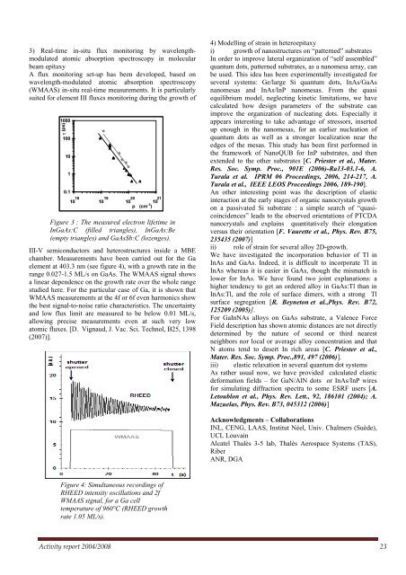
3) Real-time in-situ flux monitoring by wavelengthmodulatedatomic absorption spectroscopy in molecularbeam epitaxyA flux monitoring set-up has been developed, based onwavelength-modulated atomic absorption spectroscopy(WMAAS) in-situ real-time measurements. It is particularlysuited for element III fluxes monitoring during the growth of1000τ (ps)1001010.11E+1810 18 1E+1910 19 1E+2010 1E+2110 p (cm -3 )Figure 3 : The measured electron lifetime inInGaAs:C (filled triangles), InGaAs:Be(empty triangles) and GaAsSb:C (lozenges).III-V semiconductors and heterostructures inside a <strong>MB</strong>Echamber. Measurements have been carried out for the Gaelement at 403.3 nm (see figure 4), with a growth rate in therange 0.027-1.5 ML/s on GaAs. The WMAAS signal showsa linear dependence on the growth rate over the whole rangestudied here. For the particular case of Ga, it is shown thatWMAAS measurements at the 4f or 6f even harmonics showthe best signal-to-noise ratio characteristics. The uncertaintyand low flux limit are measured to be below 0.01 ML/s,allowing precise measurements even at such very lowatomic fluxes. [D. Vignaud, J. Vac. Sci. Technol, B25, 1398(2007)].4) Modelling of strain in heteroepitaxyi) growth of nanostructures on “patterned” substratesIn order to improve lateral organization of “self assembled”quantum dots, patterned substrates, as a nanomesa array, canbe used. This idea has been experimentally investigated forseveral systems: Ge/large Si quantum dots, InAs/GaAsnanomesas and InAs/InP nanomesas. From the quasiequilibrium model, neglecting kinetic limitations, we havecalculated how design parameters of the substrate canimprove the organization of nucleating dots. Especially itappears interesting to take advantage of stressors, insertedup enough in the nanomesas, for an earlier nucleation ofquantum dots as well as a stronger localization near theedges of the mesas. This study has been first performed inthe framework of NanoQUB for InP substrates, and thenextended to the other substrates [C. Priester et al., Mater.Res. Soc. Symp. Proc., 901E (2006)-Ra13-03.1-6, A.Turala et al. IPRM 06 Proceedings, 2006, 214-217, A.Turala et al., IEEE LEOS Proceedings 2006, 189-190].An other interesting point was the description of elasticinteraction at the early stages of organic nanocrystals growthon a passivated Si substrate : a simple search of “quasicoincidences”leads to the observed orientations of PTCDAnanocrystals and explains quantitatively their elongationversus their orientation [F. Vaurette et al., Phys. Rev. B75,235435 (2007)]ii) role of strain for several alloy 2D-growth.We have investigated the incorporation behavior of Tl inInAs and GaAs. Indeed, it is difficult to incorporate Tl inInAs whereas it is easier in GaAs, though the mismatch islower for InAs. We have found two joint explanations: ahigher tendency to get an ordered alloy in GaAs:Tl than inInAs:Tl, and the role of surface dimers, with a strong Tlsurface segregation [R. Beyneton et al.,Phys. Rev. B72,125209 (2005)].For GaInNAs alloys on GaAs substrate, a Valence ForceField description has shown atomic distances are not directlydetermined by the nature of second or third nearestneighbors nor local or average alloy concentration and thatN atoms tend to desert In rich areas [C. Priester et al.,Mater. Res. Soc. Symp. Proc.,891, 497 (2006)].iii) elastic relaxation in several quantum dot systemsAs rather usual now, we have provided calculated elasticdeformation fields – for GaN/AlN dots or InAs/InP wiresfor simulating diffraction spectra to some ESRF users [A.Letoublon et al., Phys. Rev. Lett., 92, 186101 (<strong>2004</strong>); A.Mazuelas, Phys. Rev. B73, 045312 (2006)]Acknowledgments – CollaborationsINL, CENG, LAAS, Institut Néel, Univ. Chalmers (Suède),UCL LouvainAlcatel Thalès 3-5 lab, Thalès Aerospace Systems (TAS),RiberANR, DGAFigure 4: Simultaneous recordings ofRHEED intensity oscillations and 2fWMAAS signal, for a Ga celltemperature of 960°C (RHEED growthrate 1.05 ML/s).<strong>Activity</strong> report <strong>2004</strong>/<strong>2008</strong> 23