Activity Report 2004-2008 (3,5 MB â 1st - IEMN
Activity Report 2004-2008 (3,5 MB â 1st - IEMN
Activity Report 2004-2008 (3,5 MB â 1st - IEMN
- No tags were found...

You also want an ePaper? Increase the reach of your titles
YUMPU automatically turns print PDFs into web optimized ePapers that Google loves.
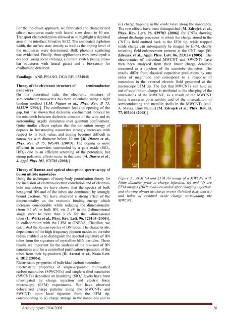
For the top-down approach, we fabricated and characterizedsilicon nanowires made with lateral sizes down to 10 nm.Transport characterization allowed us to highlight a depletedarea at the interface Si/native SiO2. The associated depletionwidth, the surface state density as well as the doping level ofthe nanowires were determined. Bulk phonons scatteringwas evidenced. Finally, three applications were developed: adecoder (using local etching), a current switch (using crossbarstructures with lateral gates) and a bio-sensor forovalbumine detection.Fundings : ANR-PNANO, DGA REI 0534048Theory of the electronic structure of semiconductornanowiresOn the theoretical side, the electronic structure ofsemiconductor nanowires has been calculated using a tightbinding method [Y.M. Niquet et al., Phys. Rev. B 73,165319 (2006)]. The confinement leads to opening of thegap, but it is shown that dielectric confinement induced bythe mismatch between dielectric constant of the wire and itssurrounding largely dominates over quantum confinement.Quite similar effects explain that the ionization energy ofdopants in freestanding nanowires strongly increases withrespect to its bulk value, and doping becomes difficult innanowires with diameter below 10 nm [M. Diarra et al.,Phys. Rev. B 75, 045301 (2007)]. The doping is moreefficient in nanowires surrounded by a gate oxide (SiO 2 ,HfO 2 ) due to an efficient screening of the potentials, butstrong polaronic effects occur in that case [M. Diarra et al.,J. Appl. Phys 103, 073703 (<strong>2008</strong>)].Theory of Raman and optical absorption spectroscopy ofboron nitride nanotubesUsing the techniques of many-body perturbation theory forthe inclusion of electron-electron correlation and of electronholeinteraction, we have shown that the spectra of bulkhexagonal BN and of the tubes are dominated by stronglybound excitons. We have observed a strong effect of thedimensionality on the excitonic binding energy whichincreases considerably while reducing the dimensionality(from 0.7 eV in bulk BN, via 2 eV in the 2-dimensionalsingle sheet to more than 3 eV for the 1-dimensionaltubes)[L. Wirtz et al., Phys. Rev. Lett. 96, 126104 (2006)].In collaboration with the LEM at ONERA, Chatillon, wecalculated the Raman spectra of BN tubes. The characteristicdependence of the high frequency phonon modes on the tuberadius enabled us to distinguish the spectral signature of BNtubes from the signature of crystalline hBN particles. Theseresults are important for the analysis of the raw-soot of BNnanotubes and for a controlled purification/separation of thetubes from their by-products [R. Arenal et al., Nano Lett.6, 1812 (2006)].Electrostatic properties of individual carbon nanotubesElectrostatic properties of single-separated multiwalledcarbon nanotubes (MWCNTs) and single-walled nanotubes(SWCNTs) deposited on insulating (SiO 2 ) layers have beeninvestigated by charge injection and electric forcemicroscopy (EFM) experiments. We have observeddelocalized charge patterns along the MWCNTs andSWCNTs upon local injection from the EFM tip,corresponding to (i) charge storage in the nanotubes and to(ii) charge trapping in the oxide layer along the nanotubes.The two effects have been distinguished [M. Zdrojek et al.,Phys. Rev. Lett. 96, 039703 (2006)] for CNTs showingabrupt discharge processes in which the charge stored in theCNT is field emitted back to the EFM tip, while trappedoxide charge can subsequently be imaged by EFM, clearlyrevealing field-enhancement patterns at the CNT caps [M.Zdrojek et al., Appl. Phys. Lett. 86, 213114 (2005)]. Theelectrostatics of individual MWCNT and SWCNTs havethen been analyzed from their linear charge densitiesmeasured as a function of the nanotube diameters. Theresults differ from classical capacitive predictions by oneorder of magnitude and correspond to a response ofnanotubes in the external electric field generated at themicroscope EFM tip. The fact that MWCNTs can hold anout-of-equilibrium charge is attributed to the charging of theinner-shells of the MWCNT, as a result of the MWCNTfinite transverse polarisability and of the intercalation ofsemiconducting and metallic shells in the MWCNTs (coll.A. Mayer, Univ Namur) [M. Zdrojek et al., Phys. Rev. B,77, 033404 (<strong>2008</strong>)].Figure 3 : AFM (a) and EFM (b) image of a MWCNT with18nm diameter prior to charge injection. (c) and (d) areEFM images (20Hz scale) recorded after charging injection,and showing abrupt discharge events (labelled d 1 ,d 2 and d 3 )and halos of residual oxide charge surrounding theMWCNT.<strong>Activity</strong> report <strong>2004</strong>/<strong>2008</strong> 26