II.3 Nano/Micro & Opto-ElectronicsIntroductionThe research activities of this task concerns advanced devices in the fields of the micro and Nano-electronics,Optoelectronics and Photonics. Up to now, the technological limitations are not completely achieved in terms ofdimension, materials, device architectures and co-integration. Moreover, this domain of research is going tochange while electronics, photonics and Electromagnetism sciences are going together to create newadvancements. Conventional top-down technological approach is continuing to reach nanometer dimensions, butbottom-up ones is also investigate by using 1D-electronics materials.These works are strongly oriented to the medium and long term and are in agreement with the national andinternational strategic and economic criteria. Indeed, whole of these research activities are supported by thenational research networks (ANR, DGA) and by the European research frameworks (FP6, FP7, ESA, MOD…). Thestriking results described after this introduction are scheduled from the micro/nano electronics to photonics via theTHz domain. Let us introduce the context for each topic of this domain.- Micro and nano-electronics: the main objectives concern the fabrication of advanced nano-electronic devices,and the improvement of the frequency limitations toward THz in the field of low noise and low power consumption(detection, amplification…), power (generation, amplification…) and high speed digital applications. The studiesconcern the optimization of the technological processes, the physical and electrical (DC and high frequency)simulations and characterizationsHigh power electronics: the activity concerns wide bandgap semiconductors such as gallium nitride andmore innovative materials (BN and diamond). The goal is the fabrication of power chips and power amplifiers formilitary and telecommunication applications. State of the art performance was obtained for devices on Si(111)substrates at 18GHz with a microwave power density of 5.1W/mm associated to a PAE of 18% and a power gain of9dB.Low power consumption electronics: we develop devices based on new materials system or newarchitectures like double gate HEMTs, ballistics devices and plasma wave transistors. State-of-the-art results onmicrowave properties of carbon nanotubes based transistors have been also obtained. For instance, we obtainedan intrinsic current gain cutoff frequency of 30 GHz establishing state-of-the-art high frequency potentialities ofCNTFETs.Non conventional nanometre-scale MOSFETs: Thanks to technological facilities and associatedexpertise, we study and fabricate alternative MOS architectures to overcome roadblocks associated to the ITRSend-of-roadmap. The present research theme focuses on the design and the fabrication of metallic Schottkysource/drain (S/D) MOSFETs, the design of a new FinFET architecture and the study of impact-ionization MOSFET(I-MOS) to overcome the subthreshold slope limitation of MOSFETs (60mV/dec). The microwave properties ofaggressively scaled Schottky S/D MOSFETs are also analysed by complementatry modelling and experimentalapproaches.Metamaterial: At the boundaries of electronics, electromagnetism and photonics, this activity isstrengthened and significant results was obtained since the last four years. This topic tends to address crucialbreakthroughs like the demonstration of negative refraction at microwave frequencies, a novel approach forcloaking at Terahertz frequencies or still the experimental verification of focusing by a Photonic crystal. In this lastaspect, outstanding results were achieved experimentally and theoretically in the field of left-handedelectromagnetism.- Optoelectronics and photonics: this thematic includes generation and detection of terahertz (THz) signals forspectroscopy, imagery, and telecommunications is investigated along an optoelectronic approach by combininglaser sources and ultra-fast optoelectronic devices.Optoelectronics: Microwave photonics affords new potentialities in the optical processing of microwavesignals. We applied it mainly to the optical beam forming of wide instantaneous bandwidth phased array antennas.Specific devices have been so studied and fabricated; as high speed optical switching matrices and detectors.Nanophotonics: using III-V semiconductor material line allows the mixing of passive and activefunctionalities. We capitalize on the compactness and the high optical confinement of these circuits i) to decreasesurface areas requested for passive integrated optics circuits, ii) to decrease interaction volume required forelectro-optic functions and iii) to increase non-linear effects.- Modelling: besides of all these experimental topics, this activity is to develop physical models and to implementthem in simulation tools. All important aspects of micro and nanoelectronics have been considered: technologicalfabrication processes, physical mechanisms of device operation and performance of devices and circuits. A widevariety of devices have been studied: field effect transistors, ferroelectric memories, semiconductor lasers.<strong>Activity</strong> report <strong>2004</strong>/<strong>2008</strong> 41
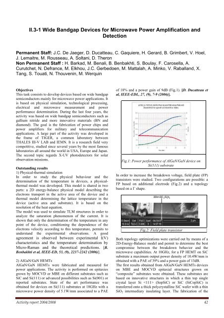
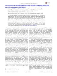
II.3-1 Wide Bandgap Devices for Microwave Power Amplification andDetectionPermanent Staff: J.C. De Jaeger, D. Ducatteau, C. Gaquiere, H. Gerard, B. Grimbert, V. Hoel,J. Lemaitre, M. Rousseau, A. Soltani, D. TheronNon Permanent Staff : H. Barkad, M. Benali, B. Benbakhti, S. Boulay, F. Carosella, A.Curutchet, N. Defrance, M. Elkhou, J.C. Gerbedoen, M. Mattalah, A. Minko, V. Raballand, X.Tang, S. Touati, N. Thouvenin, M. WerquinObjectivesThis task consists to develop devices based on wide bandgapsemiconductors mainly for microwave power applications. Itis based on physical simulation, technological processing,electrical and microwave measurement and powerperformance determination. During the last four years, theactivity was based on wide bandgap semiconductors such asgallium nitride and more innovative materials (BN anddiamond). The goal is the fabrication of power chips andpower amplifiers for military and telecommunicationapplications. A large part of the activity was developed inthe frame of TIGER, a common laboratory betweenTHALES III-V LAB and <strong>IEMN</strong>. It is a research field verycompetitive, studied since several years by the most famouslaboratories all around the world in USA, Europe and Japan.The second topic regards X-UV photodetectors for solarobservation missions.Outstanding results1) Physical-thermal simulationIn order to study the physical behaviour and thedetermination of the temperature in devices, a physicalthermalmodel was developed. This model is shared in twoparts: a 2D energy-balance physical model describing theelectrons transport in the active area of the device and athermal model determining the lattice temperature in thedevice (active area and substrate). It is based on theresolution of the heat equation.The model was used to simulate TLM structures in order toanalyze the saturation phenomenon of the current. It isshown that only the determination of the temperature in anypoint of the device, conditioning the dependence of theelectrons velocity according to this temperature, permits tounderstand the experimental observations. A goodagreement is observed between experimental I(V)characteristics and the temperature determination byMicro-Raman and the theoretical predictions. [B.Benbakhti et al, IEEE-ED, 53, (9), 2237-2242 (2006)].2) AlGaN/GaN HEMTsAlGaN/GaN HEMTs were fabricated and measured forpower applications. The activity is performed on epitaxiesgrown by MOCVD or <strong>MB</strong>E on different substrates such asSiC and Si(111) or advanced possibilities such as Si(001) orreported substrates. State of the art performance wasobtained for devices on Si(111) substrates at 18GHz with amicrowave power density of 5.1W/mm associated to a PAEof 18% and a power gain of 9dB (Fig.1). [D. Ducatteau etal, IEEE-EDL, 27, (9), 7-9 (2006)].Fig.1: Power performance of AlGaN/GaN device onSi(111) substrateIn order to increase the breakdown voltage, field plate (FP)transistors were studied. Two configurations are possible: aFP based on additional electrode (Fig.2) and a topologybased on a Γ shape.GFP300nm SiO 2/Si 3N 4Fig.2: Field plate transistorBoth topology optimizations were carried out by means of a2D-Energy-Balance model and permit to determine the bestcompromise between the breakdown behavior and themicrowave capabilities. At 10GHz, for a FP HEMT on SiCsubstrate a maximum output power density of 10.4W/mm isobtained with a PAE of 39% and a power gain of 13dB.The first results obtained from AlGaN/GaN HEMTs deviceson <strong>MB</strong>E and MOCVD epitaxial structures grown on“composite” substrates were obtained. These substrates arebased on innovative structures in which a thin top singlecrystal layer Si (SopSiC) or SiC (SiCopSiC) istransferred onto a thick polycrystalline SiC wafer with a thinSiO 2 intermediary insulating layer. The fabrication of theD<strong>Activity</strong> report <strong>2004</strong>/<strong>2008</strong> 42