Activity Report 2004-2008 (3,5 MB â 1st - IEMN
Activity Report 2004-2008 (3,5 MB â 1st - IEMN
Activity Report 2004-2008 (3,5 MB â 1st - IEMN
- No tags were found...

You also want an ePaper? Increase the reach of your titles
YUMPU automatically turns print PDFs into web optimized ePapers that Google loves.
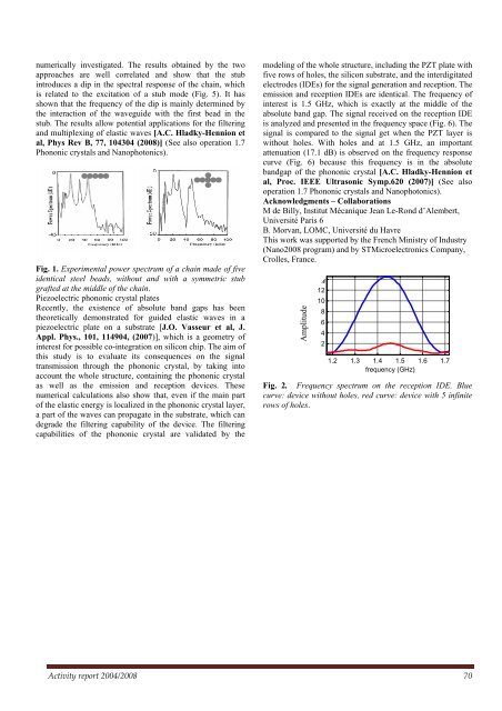
numerically investigated. The results obtained by the twoapproaches are well correlated and show that the stubintroduces a dip in the spectral response of the chain, whichis related to the excitation of a stub mode (Fig. 5). It hasshown that the frequency of the dip is mainly determined bythe interaction of the waveguide with the first bead in thestub. The results allow potential applications for the filteringand multiplexing of elastic waves [A.C. Hladky-Hennion etal, Phys Rev B, 77, 104304 (<strong>2008</strong>)] (See also operation 1.7Phononic crystals and Nanophotonics).Fig. 1. Experimental power spectrum of a chain made of fiveidentical steel beads, without and with a symmetric stubgrafted at the middle of the chain.Piezoelectric phononic crystal platesRecently, the existence of absolute band gaps has beentheoretically demonstrated for guided elastic waves in apiezoelectric plate on a substrate [J.O. Vasseur et al, J.Appl. Phys., 101, 114904, (2007)], which is a geometry ofinterest for possible co-integration on silicon chip. The aim ofthis study is to evaluate its consequences on the signaltransmission through the phononic crystal, by taking intoaccount the whole structure, containing the phononic crystalas well as the emission and reception devices. Thesenumerical calculations also show that, even if the main partof the elastic energy is localized in the phononic crystal layer,a part of the waves can propagate in the substrate, which candegrade the filtering capability of the device. The filteringcapabilities of the phononic crystal are validated by themodeling of the whole structure, including the PZT plate withfive rows of holes, the silicon substrate, and the interdigitatedelectrodes (IDEs) for the signal generation and reception. Theemission and reception IDEs are identical. The frequency ofinterest is 1.5 GHz, which is exactly at the middle of theabsolute band gap. The signal received on the reception IDEis analyzed and presented in the frequency space (Fig. 6). Thesignal is compared to the signal get when the PZT layer iswithout holes. With holes and at 1.5 GHz, an importantattenuation (17.1 dB) is observed on the frequency responsecurve (Fig. 6) because this frequency is in the absolutebandgap of the phononic crystal [A.C. Hladky-Hennion etal, Proc. IEEE Ultrasonic Symp.620 (2007)] (See alsooperation 1.7 Phononic crystals and Nanophotonics).Acknowledgments – CollaborationsM de Billy, Institut Mécanique Jean Le-Rond d’Alembert,Université Paris 6B. Morvan, LOMC, Université du HavreThis work was supported by the French Ministry of Industry(Nano<strong>2008</strong> program) and by STMicroelectronics Company,Crolles, France.AmplitudeA121086421.2 1.3 1.4 1.5 1.6 1.7frequency (GHz)Fig. 2. Frequency spectrum on the reception IDE. Bluecurve: device without holes, red curve: device with 5 infiniterows of holes.<strong>Activity</strong> report <strong>2004</strong>/<strong>2008</strong> 70