Integrated Transceivers for Optical Wireless Communications
Integrated Transceivers for Optical Wireless Communications
Integrated Transceivers for Optical Wireless Communications

You also want an ePaper? Increase the reach of your titles
YUMPU automatically turns print PDFs into web optimized ePapers that Google loves.
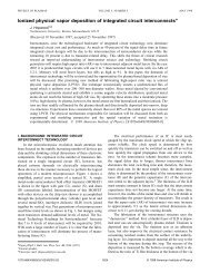
176 IEEE JOURNAL OF SELECTED TOPICS IN QUANTUM ELECTRONICS, VOL. 11, NO. 1, JANUARY/FEBRUARY 2005Fig. 6.Photodetector structure.Fig. 5(b) shows an eye diagram <strong>for</strong> a device that is biasedusing a constant current driver and modulated using a 310-Mb/spseudorandom binary sequence. This shows that the RCLEDshave sufficient bandwidth <strong>for</strong> this application. Fig. 5(c) showsthe simulated and actual measured beam profile from a typicaldevice. The measured profile is a closest match to the simulatedresult <strong>for</strong> the highly detuned devices, showing the particulararray uses a highly detuned portion of the wafer.B. Detectors1) Detector Structure: The system requires a close-packedarray of hexagonal detectors that are illuminated through theirsubstrate, and the per<strong>for</strong>mance of these detectors is one of thekey design constraints. In a system where the transmitter beam islarger than the receiver collection aperture, the power collectedwill usually be proportional to the detector area <strong>for</strong> any givenoptical system. However, increasing detector area increasesthe capacitance presented to the system preamplifiers, whichreduces the available bandwidth. A major focus of this workhas been in optimizing detector structures <strong>for</strong> this free-spaceapplication. An optimum detector <strong>for</strong> optical wireless wouldbalance transit time and capacitance controlled bandwidth andachieve maximum area <strong>for</strong> a given bandwidth. Epitaxiallygrown structures such as that grown here allow independentcontrol of depletion width and field by the growth of Intrinsic(I) regions of the correct thickness, so that this should bepossible. Preliminary modeling of an InGaAs p-i-n structureshows that a 30- m I region could offer bandwidths of 1GHz <strong>for</strong> a 1-mm device (assuming a 50- amplifier inputimpedance). This is a <strong>for</strong>midable challenge, due to the problemsin controlling doping in such thick structures, and in the devicesgrown <strong>for</strong> this work, the I region was limited to a 5- m layer.Optimized detectors might also include filtering layers to reducethe noise from optically broadband ambient illumination, andpreliminary structures that show filtering action have beengrown [12]. However, these proved to be too capacitive andsimpler p-i-n structures were grown <strong>for</strong> the demonstrator.Fig. 6 shows the p-i-n photodiode structures grown <strong>for</strong> thereceiver subsystem. These are substrate illuminated InGaAs/InPp-i-n diodes grown on InP substrates by MOVPE. These areFig. 7.Seven-channel detector array suitable <strong>for</strong> flip-chip bonding.designed <strong>for</strong> substrate illumination and operation in the rangefrom 980 to beyond 1500 nm. The structure incorporates a topcontact that also acts as a mirror, which ensures that unabsorbedphotons are reflected back into the detectors, thus increasingtheir responsivity.Wafers were processed into seven-element hexagonal pitcharrays, with close-packed devices on a 500- m pitch. Devicesize and, hence, pitch was chosen from optical design considerationsand to ensure the maximum capacitance presented to thereceivers was within their design specification.2) Device Per<strong>for</strong>mance: Devices typically have a measuredcapacitance of 5.2 pF (at 4-V reverse bias) compared with acalculated value of 5.1 pF <strong>for</strong> a fully depleted I region. The slightdiscrepancy is due to the reduced bias voltage (4 V) comparedto that required to fully deplete the I region (estimated to beapproximately 8 V). This is a factor of five lower than typicalcommercial devices, showing the importance of optimizingdevices <strong>for</strong> this application. The measured responsivity was 0.39A/W at 980 nm, compared with a theoretical maximum of 0.79A/W. Two factors contribute to the reduction in responsivity: theInP substrate has significant absorption at this wavelength, andthe Fresnel losses ( 30 ) as light enters the semiconductorsubstrate reduce the illumination incident on the p-i-n structure.An estimate of the likely reduction these two effects produceleads us to believe the detectors are operating efficiently.Fig. 7 shows a picture of a seven-channel detector array witha 500- m pitch that is suitable <strong>for</strong> flip-chip bonding. As was thecase <strong>for</strong> the emitters, a number of protective metal layers weregrown on top of the basic detector structure in order to stop golddiffusing into the solder bumps.V. SILICON DESIGNA. TransmittersFig. 8(a) shows a block diagram of the RCLED driver circuitthat is used to drive each source. The core function of the driveris voltage-to-current conversion to produce modulating <strong>for</strong>wardcurrent from a voltage data signal. The modulation circuit inthe driver consists of a voltage-to-current transducer and a