Integrated Transceivers for Optical Wireless Communications
Integrated Transceivers for Optical Wireless Communications
Integrated Transceivers for Optical Wireless Communications

You also want an ePaper? Increase the reach of your titles
YUMPU automatically turns print PDFs into web optimized ePapers that Google loves.
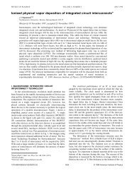
178 IEEE JOURNAL OF SELECTED TOPICS IN QUANTUM ELECTRONICS, VOL. 11, NO. 1, JANUARY/FEBRUARY 2005Fig. 9.Transimpedance amplifier circuit diagram.B. Receivers1) Transimpedance Amplifier: A major ef<strong>for</strong>t has been thedesign of the receiver preamplifier circuit, shown in Fig. 9. Thedetails of its design are outlined in [18]. A transimpedance amplifierstructure is used and consists of a three-stage voltage amplifierwith shunt resistive feedback. This approach provides thebest compromise in terms of noise, gain, and bandwidth, all ofwhich are influenced by the capacitance of the detector. Eachstage of the amplifier is identical and consists of an inverter stagewith diode-connected load. This topology has several design advantages.The inverter, compared to a single device, produces ahigher transconductance <strong>for</strong> a given bias current. Furthermore,the diode-connected load is used to trade off the gain of the unloadedinverter <strong>for</strong> increased small-signal bandwidth. The transimpedancebandwidth is governed by the input capacitance,open loop gain of the amplifier, and the feedback resistance. Inorder to account <strong>for</strong> variances in the detector capacitance andparasitics, a variable feedback resistor is implemented using apositive channel MOS (PMOS) transistor biased in the linear region.The resistance can be varied by applying a voltage biasto the gate of the transistor in order to achieve the required bandwidthand maintain stability over a range of 2–10 pF of capacitanceat the input.The preamplifier circuit was fabricated using a 0.7- mCMOS process technology, offered through the Europracticeinitiative. With a total input capacitance (including detectorand parasitics) of 10 pF, the transimpedance amplifier achievesa measured bandwidth of 217 MHz and transimpedance gainof 4.2 k . This compares extremely favorably with [19] whichreports a 156-Mb/s receiver with a 2.5-pF input capacitance.Noise per<strong>for</strong>mance of the circuit was measured by comparingthe output noise spectra with and without input signal in orderto remove the effect of measurement noise, as proposed byCarruthers [20]. The measured input-referred noise currentdensity is 5.92 pA Hz. At a bandwidth of 217 MHz, usingthe measured detector responsivity of 0.39 A/W, this impliesa sensitivity of approximately 29 dBm at 980 nm. Fig. 10(a)shows a 310-Mb/s eye diagram receiver output, showing goodper<strong>for</strong>mance at this data rate. Calculations indicate that avariation in optical power of approximately 22 dB can be accommodatedby the preamplifier, but due to the limited sourcepower available, this was only verified by measurement over a7.5-dB range.Fig. 10. Eye diagrams <strong>for</strong> transimpedance amplifier operating at 310 Mb/s andlater design operating at 1 Gb/s.2) Gigabit Receiver: In order to investigate extending theproposed receiver architecture to Gb/s data rates, a receiver ICoperating at 1 Gb/s was developed and realized in a 0.35- mCMOS process. The chip includes two transimpedance amplifierstages; one is a common-source input stage, and the othera current-mode common-gate input stage. The low input resistanceof the common-gate stage has many potential advantages,as the large detector capacitance can be decoupled fromthe bandwidth and gain of the preamplifier, ultimately leadingto lower noise. Theoretical analysis presented in [21] showsthat the per<strong>for</strong>mance improvement offered by the common-gatestage is limited when implementing the receiver in a standardCMOS technology operating at a single, low supply voltage.Furthermore, isolating the large photodiode capacitances expectedin optical wireless receivers can lead to large junctioncapacitances that further degrade per<strong>for</strong>mance and hinder designoptimization. Electrical measurements were carried out onboth preamplifier topologies using a detector emulation circuitat the input of each channel with an associated capacitance of 6pF. Best results were achieved on the common-source channel.The common-source preamplifier achieves a gain of 44.6 dB,3-dB bandwidth of 500 MHz, and an input-referred currentnoise power spectral density (PSD) of 14.8 pA Hz; good eyeopenings have been demonstrated at bit rates up to 1 Gb/s asshown in Fig. 10(b).