

2 The scaling of MOSFETs, Moore's law, and ITRS
2 The scaling of MOSFETs, Moore's law, and ITRS
2 The scaling of MOSFETs, Moore's law, and ITRS

You also want an ePaper? Increase the reach of your titles
YUMPU automatically turns print PDFs into web optimized ePapers that Google loves.
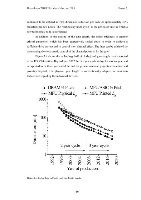
<strong>The</strong> <strong>scaling</strong> <strong>of</strong> <strong>MOSFETs</strong>, Moore’s <strong>law</strong>, <strong>and</strong> <strong>ITRS</strong> Chapter 2continued to be defined as 70% dimension reduction per node or approximately 50%reduction per two nodes. <strong>The</strong> “technology-node-cycle” is the period <strong>of</strong> time in which anew technology node is introduced.In addition to the <strong>scaling</strong> <strong>of</strong> the gate length, the oxide thickness is anothercritical parameter, which has been aggressively scaled down in order to achieve asufficient drive current <strong>and</strong> to control short channel effect. <strong>The</strong> later can be achieved bymaintaining the electrostatic control <strong>of</strong> the channel potential by the gate.Figure 2:4 shows the technology half pitch (hp) <strong>and</strong> gate length trends adoptedin the <strong>ITRS</strong>’03 edition. Beyond year 2007 the two year cycle delays by another year <strong>and</strong>is expected to be three years until the end the present roadmap projection time-line <strong>and</strong>probably beyond. <strong>The</strong> physical gate length is conventionally adapted as minimumfeature size regarding the individual devices.1000DRAM ½ PitchMPU Physical L gMPU/ASIC ½ PitchMPU Printed L gDimension [nm]100102 year cycle 3 year cycle1199219962000200420082012Year <strong>of</strong> production20162020Figure 2:4 Technology half-pitch <strong>and</strong> gate length trends.16


