<strong>The</strong> <strong>scaling</strong> <strong>of</strong> <strong>MOSFETs</strong>, Moore’s <strong>law</strong>, <strong>and</strong> <strong>ITRS</strong> Chapter 2is still a need for ‘total process optimization’ [2:35] in order to use the currentfabrication technology. For example, better designed doping pr<strong>of</strong>iles in the channel,improved gate patterning (minimum LER), shallow junction formation to reducesource-drain sheet resistance, <strong>and</strong> optimization <strong>of</strong> the gate oxide (oxynitride) bycontrolling the amount <strong>of</strong> nitrogen, are some <strong>of</strong> the process-optimization steps that canbe exploited. In addition to process optimization, the introduction <strong>of</strong> strained silicon inthe channel to enhance carrier transport, <strong>and</strong> introduction <strong>of</strong> high-κ materials to replacesilicon dioxide as an insulator will improve the chances <strong>of</strong> using conventional<strong>MOSFETs</strong> at the 65 nm technology node <strong>and</strong> possibly beyond.Apart from the 25 nm gate length MOSFET, which gives a realistic hope <strong>of</strong>realizing the 65 nm technology node by 2007, there have also been researchdemonstrations <strong>of</strong> smaller gate length devices. For example, conventional <strong>MOSFETs</strong>with gate lengths 15 nm [2.36], <strong>and</strong> 16 nm [2.37], which are required for hp45 nmtechnology node; 14 nm [2.38] for hp32 nm <strong>and</strong> 6 nm [2.39], 8 nm [2.40] <strong>and</strong> 10 nm[2.41] required for the hp22 nm technology node, have been fabricated <strong>and</strong> reported,delivering promising device parameters.<strong>The</strong>re is, however, growing consensus among the industry <strong>and</strong> researchcommunities alike, that in the 45 nm technology node <strong>and</strong> beyond, it will becomenecessary to replace the conventional <strong>MOSFETs</strong> with novel device architectures, siliconon insulator (SOI), multiple gate FETs <strong>and</strong> wide application technology boosters suchas strained silicon for carrier transport enhancement, high-κ gate stack, metal gates, etc.2.3 Factors limiting the <strong>scaling</strong> <strong>of</strong> conventional MOSFETSome <strong>of</strong> the technology advances enabled the <strong>scaling</strong> <strong>of</strong> conventional<strong>MOSFETs</strong> to decananometre dimensions were discussed in the previous sections.Unfortunately, even with all these advances the <strong>scaling</strong> <strong>of</strong> conventional <strong>MOSFETs</strong>whilst which maintaining good performance becomes increasingly difficult over time.Although the electronics industry has benefited from continuous <strong>scaling</strong> over the lastthree decades or so, the present trends indicate that the <strong>scaling</strong> <strong>of</strong> the conventional<strong>MOSFETs</strong> is fast approaching the end <strong>of</strong> its useful life time.<strong>The</strong> optimistic prediction <strong>of</strong> the 2003 edition <strong>of</strong> the <strong>ITRS</strong> that <strong>scaling</strong> willcontinue until 2018 <strong>and</strong> beyond, is challenged by some fundamental limitations.Quantum mechanical effects such as carrier confinement <strong>and</strong> tunnelling, the26
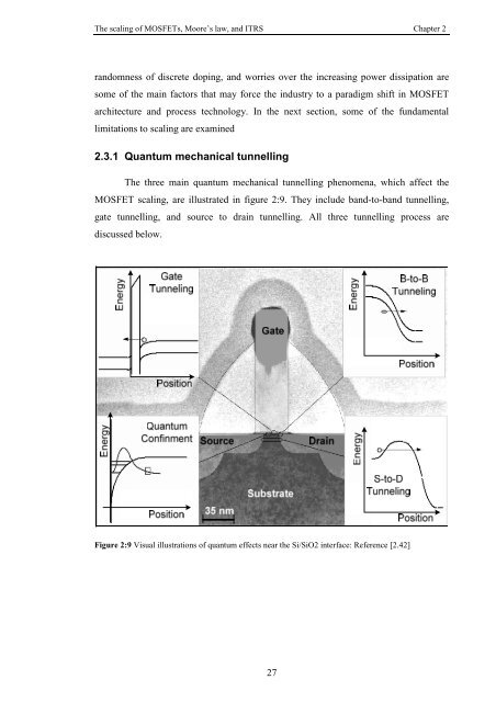
<strong>The</strong> <strong>scaling</strong> <strong>of</strong> <strong>MOSFETs</strong>, Moore’s <strong>law</strong>, <strong>and</strong> <strong>ITRS</strong> Chapter 2r<strong>and</strong>omness <strong>of</strong> discrete doping, <strong>and</strong> worries over the increasing power dissipation aresome <strong>of</strong> the main factors that may force the industry to a paradigm shift in MOSFETarchitecture <strong>and</strong> process technology. In the next section, some <strong>of</strong> the fundamentallimitations to <strong>scaling</strong> are examined2.3.1 Quantum mechanical tunnelling<strong>The</strong> three main quantum mechanical tunnelling phenomena, which affect theMOSFET <strong>scaling</strong>, are illustrated in figure 2:9. <strong>The</strong>y include b<strong>and</strong>-to-b<strong>and</strong> tunnelling,gate tunnelling, <strong>and</strong> source to drain tunnelling. All three tunnelling process arediscussed below.Figure 2:9 Visual illustrations <strong>of</strong> quantum effects near the Si/SiO2 interface: Reference [2.42]27
- Page 5 and 6: The scaling of MOSFETs, Moore’s l
- Page 8 and 9: The scaling of MOSFETs, Moore’s l
- Page 10 and 11: The scaling of MOSFETs, Moore’s l
- Page 13 and 14: The scaling of MOSFETs, Moore’s l
- Page 15 and 16: The scaling of MOSFETs, Moore’s l
- Page 17 and 18: The scaling of MOSFETs, Moore’s l
- Page 19: The scaling of MOSFETs, Moore’s l
- Page 23 and 24: The scaling of MOSFETs, Moore’s l
- Page 25 and 26: The scaling of MOSFETs, Moore’s l
- Page 27 and 28: The scaling of MOSFETs, Moore’s l
- Page 29 and 30: The scaling of MOSFETs, Moore’s l
- Page 31 and 32: The scaling of MOSFETs, Moore’s l
- Page 33 and 34: The scaling of MOSFETs, Moore’s l
- Page 35 and 36: The scaling of MOSFETs, Moore’s l
- Page 37 and 38: The scaling of MOSFETs, Moore’s l
- Page 39 and 40: The scaling of MOSFETs, Moore’s l