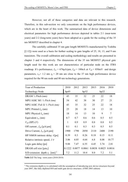
<strong>The</strong> <strong>scaling</strong> <strong>of</strong> <strong>MOSFETs</strong>, Moore’s <strong>law</strong>, <strong>and</strong> <strong>ITRS</strong> Chapter 2However, not all <strong>of</strong> these categories <strong>and</strong> data are relevant to this research.<strong>The</strong>refore, in this sub-section we only concentrate on the high performance devices,which are in the heart <strong>of</strong> this work. <strong>The</strong> summarised data <strong>of</strong> device dimensions <strong>and</strong>electrical parameters for high performance devices depicted in tables 2:1 (near-termyears) <strong>and</strong> 2:2 (long-term years) have been adopted as a guide for the <strong>scaling</strong> <strong>of</strong> the 35nm MOSFET described in chapter 4.<strong>The</strong> carefully calibrated 35 nm gate length <strong>MOSFETs</strong> manufactured by Toshiba[2.12]) were used as a basis for further <strong>scaling</strong> to gate lengths <strong>of</strong> 25, 18, 13, <strong>and</strong> 9 nmtransistors. <strong>The</strong> overall calibration <strong>and</strong> <strong>scaling</strong> methodology <strong>and</strong> results are presented inchapter 3 <strong>and</strong> 4 respectively. <strong>The</strong> dimensions <strong>of</strong> the 35 nm MOSFET physical gatelength used for this work are not characteristics <strong>of</strong> particular node on the <strong>ITRS</strong>roadmap. It’s performance, I on = 676µA/µm, I <strong>of</strong>f = 100nA at V dd = 850mV <strong>and</strong> designparameters, t ox = 1.2 nm x j = 20 nm are close to the 37 nm high performance devicerequired for the 90 nm node <strong>and</strong> 80 nm technology generations.Year <strong>of</strong> Production 2010 2012 2013 2015 2016 2018Technology Node hp45 hp32 hp22DRAM ½ Pitch (nm) 45 35 32 25 22 18MPU/ASIC M1 ½ Pitch (nm) 54 42 38 30 27 21MPU/ASIC Poli Si ½ Pitch (nm) 45 35 32 25 22 18MPU Printed L g (nm) 25 20 18 14 13 10MPU Physical L g (nm) 18 14 13 10 9 7Equivalent t ox (nm) 0.7 0.7 0.6 0.6 0.5 0.5V dd (HP) (V) 1 0.9 0.9 0.8 0.8 0.5Off current , I <strong>of</strong>f [µA/µm] 0.1 0.1 0.3 0.3 0.5 0.5Drive Current, I on [µA/µm] 1900 1790 2050 2110 2400 2190HP NMOS intrinsic delay τ [ps] 0.39 0.3 0.26 0.18 0.15 0.11Relative intrinsic speed, 1/τ 3.06 4.05 4.64 6.8 8.08 10.77Logic gate delay [ps] 9.88 7.47 6.55 4.45 3.74 2.81DRAM cell size [µm 2 ] 0.1222 0.0077 0.0061 0.0038 0.0025 0.0016S/D extension depth x j [nm] ‡ 7.2 11.2 10.4 8.0 7.2 5.1Table 2:2 <strong>The</strong> long - term years (2010-2018)‡ <strong>The</strong> extension depth (x j ) is calculated with the assumption <strong>of</strong> introducing new device structures beyondyear 2007, like fully depleted SOI <strong>and</strong> multi gate device structures. (<strong>ITRS</strong> 2003 edition)14
<strong>The</strong> <strong>scaling</strong> <strong>of</strong> <strong>MOSFETs</strong>, Moore’s <strong>law</strong>, <strong>and</strong> <strong>ITRS</strong> Chapter 2Although the electronics industry prefers to continue as long as possible with the<strong>scaling</strong> <strong>of</strong> conventional <strong>MOSFETs</strong>, there is “Red Brick Wall” to this process unlessthere is a major technological breakthrough. High channel doping, which degrades thedevice performance, <strong>and</strong> ultra thin gate oxides, which introduce unacceptable gateleakage, are likely to prompt a replacement to conventional <strong>MOSFETs</strong> somewherebeyond the 65nm technology node. Among the replacement c<strong>and</strong>idates are, for example,ultra-thin body SOI <strong>and</strong> multiple gate devices complimented by the introduction <strong>of</strong>strained silicon in the channel region to enhance the carrier mobility, <strong>and</strong> highpermittivity materials in the gate stack in order to suppress gate leakage. Some <strong>of</strong> thecritical <strong>scaling</strong> limitation factors will be examined more closely in the next sections <strong>of</strong>this chapter.2.1.4 <strong>The</strong> <strong>scaling</strong> factors <strong>and</strong> technology trends<strong>The</strong> <strong>scaling</strong> factor <strong>of</strong> κ ≈ 2, related to a 70% size reduction <strong>of</strong> the majortechnology nodes every two years, has been adapted for the linear <strong>scaling</strong> <strong>of</strong> devicedimensions in this work. <strong>The</strong> other <strong>scaling</strong> constant, αfor the electric field <strong>and</strong>potential used in the generalised <strong>scaling</strong> scenario [2:10] is not specified on the roadmap. However, it can be calculated from the supply voltages (V dd ), which are specifiedin the roadmap for corresponding feature sizes <strong>and</strong> the linear <strong>scaling</strong> factor κ as:α V 'V ' = V ⇒ α = κ(2.3)κ V'V is the new supply voltage given in the technology roadmap <strong>and</strong> V is the supplyvoltage <strong>of</strong> the previous generation. It should be noted that in some papers [2.13], thelinear <strong>scaling</strong> factor has been decomposed to separate dimensional <strong>scaling</strong> parameters inthe so called “selective <strong>scaling</strong> case”, which introduces different values for vertical,horizontal, <strong>and</strong> lateral dimensions multipliers. However, in this work, the generalized<strong>scaling</strong> rule has been adopted as a principal guiding rule for device <strong>scaling</strong>. A review <strong>of</strong>the different <strong>scaling</strong> approaches is presented in the next section.Unlike the previous editions <strong>of</strong> <strong>ITRS</strong>, no prediction <strong>of</strong> the technologyacceleration has been made in its latest edition (<strong>ITRS</strong>’03). Also, as illustrated in figure2.4, in the last <strong>ITRS</strong> edition, the technology generations are predicted to shift from thepresent two-year cycle to a three-year cycle trend around 2007. <strong>The</strong> technology node15
- Page 5 and 6: The scaling of MOSFETs, Moore’s l
- Page 10 and 11: The scaling of MOSFETs, Moore’s l
- Page 13 and 14: The scaling of MOSFETs, Moore’s l
- Page 15 and 16: The scaling of MOSFETs, Moore’s l
- Page 17 and 18: The scaling of MOSFETs, Moore’s l
- Page 19 and 20: The scaling of MOSFETs, Moore’s l
- Page 21 and 22: The scaling of MOSFETs, Moore’s l
- Page 23 and 24: The scaling of MOSFETs, Moore’s l
- Page 25 and 26: The scaling of MOSFETs, Moore’s l
- Page 27 and 28: The scaling of MOSFETs, Moore’s l
- Page 29 and 30: The scaling of MOSFETs, Moore’s l
- Page 31 and 32: The scaling of MOSFETs, Moore’s l
- Page 33 and 34: The scaling of MOSFETs, Moore’s l
- Page 35 and 36: The scaling of MOSFETs, Moore’s l
- Page 37 and 38: The scaling of MOSFETs, Moore’s l
- Page 39 and 40: The scaling of MOSFETs, Moore’s l