

2 The scaling of MOSFETs, Moore's law, and ITRS
2 The scaling of MOSFETs, Moore's law, and ITRS
2 The scaling of MOSFETs, Moore's law, and ITRS

You also want an ePaper? Increase the reach of your titles
YUMPU automatically turns print PDFs into web optimized ePapers that Google loves.
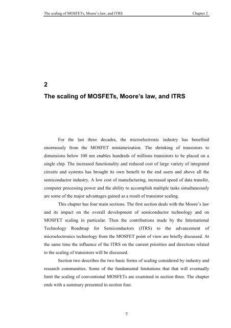
<strong>The</strong> <strong>scaling</strong> <strong>of</strong> <strong>MOSFETs</strong>, Moore’s <strong>law</strong>, <strong>and</strong> <strong>ITRS</strong> Chapter 2<strong>The</strong> second important feature associated with the Moore’s <strong>law</strong> is cost. It is ageneral rule that the goal <strong>of</strong> every manufacturing community is maximizing the pr<strong>of</strong>itwhile minimizing the cost <strong>of</strong> production. <strong>The</strong> electronics industry is not unique in this.In fact the primary implication <strong>of</strong> the Moore’s <strong>law</strong> is the reduction <strong>of</strong> manufacturingcost per function <strong>and</strong> at the same time to increase the functionality per chip. As it can beseen from figure 2:2 the reduction in cost-per-function according to the latest <strong>ITRS</strong>edition, is roughly 50% in about two years.<strong>The</strong> third important implication <strong>of</strong> Moore’s <strong>law</strong> is the performance factor.Performance in general can be measured, for example, by the speed <strong>of</strong> typicalmicroprocessors. Figure 2:3 shows the increasing speed <strong>and</strong> density <strong>of</strong> present <strong>and</strong>future generations <strong>of</strong> technology nodes. <strong>The</strong> <strong>of</strong>f-chip frequency is the maximum input<strong>and</strong> output signal frequency to board peripheral buses <strong>of</strong> high performance devices[2.4]. <strong>The</strong> <strong>of</strong>f-chip frequency is increasing faster than the on-chip local frequency nearthe end <strong>of</strong> the current edition <strong>of</strong> the <strong>ITRS</strong>.On-Chip (local) frequencyOff-Chip frequencyTransistors in SRAMTransistors in Logic1.6x10 4Frequency [ MHz ]10 5 1.2x10 410 48.0x10 34.0x10 30.010 320012004200720102013Year <strong>of</strong> production20162019Number <strong>of</strong> transistors [x 10 6 ]Figure 2:3 <strong>The</strong> technology trends <strong>of</strong> on-chip local clock, <strong>of</strong>f-chip frequency, chip density in SRAM <strong>and</strong>Logic gats (transistors per cm 2 ). <strong>ITRS</strong> 2004 Edition11
<strong>The</strong> <strong>scaling</strong> <strong>of</strong> <strong>MOSFETs</strong>, Moore’s <strong>law</strong>, <strong>and</strong> <strong>ITRS</strong> Chapter 2In general the frequency is related to the speed <strong>of</strong> switching <strong>of</strong> the individual<strong>and</strong> simple logic components determined by CMOS transistors which is inverselyproportional to the delay time that takes to propagate signal through the inverter. <strong>The</strong>inverter delay time formulated as [2.8]:τint= Rsw ( Cin + Cout)(2.1)Where τ int is the inverter delay time, R sw is the switching resistance, C in inputcapacitance, C out the output capacitance, <strong>and</strong> in equation 2.2, C gate is the gatecapacitance. This inverter delay time can be used as approximation <strong>of</strong> the CMOS delaytime which is calculated empirically as: [2.9]VDDτ = Cgate(2.2)IdsatAccording to the generalised <strong>scaling</strong> [2.10, 2.11],τ is inversely proportional to the<strong>scaling</strong> factor, which allows faster circuit operations. Figure 2:2 also depicts theincrease in the density <strong>of</strong> transistors in SRAM <strong>and</strong> Logic circuits. Density is inverselyproportional to the total chip area (1/A). <strong>The</strong>refore, density will increase by κ 2 as aresult <strong>of</strong> <strong>scaling</strong>, where κ ≈ 2 is the <strong>scaling</strong> constant (see section 2.1.4).2.1.3 <strong>The</strong> International Technology Roadmap for Semiconductors<strong>The</strong> technology roadmap is an ambitious document widely used as a guidingreference for advanced semiconductor device research <strong>and</strong> manufacturing purposes. <strong>The</strong>latest edition (2003) † <strong>of</strong> international technology roadmap for semiconductors (<strong>ITRS</strong>),updated in 2004, sets main objectives <strong>and</strong> targets to 2018. Based on research from thesemiconductor industry <strong>and</strong> academia, the latest edition <strong>of</strong> the <strong>ITRS</strong> outlines therequirements <strong>and</strong> identifies the challenges which allow Moore’s <strong>law</strong> to be maintainedover the next 15 years. In addition to the challenges, it also outlines the possiblesolutions to some <strong>of</strong> the problems that the industry may face <strong>and</strong> highlights the specificareas that need urgent research.Overall, the roadmap has three major contributions. <strong>The</strong> first is to identify theneeds <strong>and</strong> requirements to be met by technology solutions currently under development.<strong>The</strong> second is to recognize the existence <strong>of</strong> interim solutions for the medium termchallenges <strong>and</strong> problems <strong>and</strong> their limitations at the present time. <strong>The</strong> third important† <strong>The</strong> latest <strong>ITRS</strong> edition <strong>of</strong> 2005 has been published after the completion <strong>of</strong> this thesis12
<strong>The</strong> <strong>scaling</strong> <strong>of</strong> <strong>MOSFETs</strong>, Moore’s <strong>law</strong>, <strong>and</strong> <strong>ITRS</strong> Chapter 2However, not all <strong>of</strong> these categories <strong>and</strong> data are relevant to this research.<strong>The</strong>refore, in this sub-section we only concentrate on the high performance devices,which are in the heart <strong>of</strong> this work. <strong>The</strong> summarised data <strong>of</strong> device dimensions <strong>and</strong>electrical parameters for high performance devices depicted in tables 2:1 (near-termyears) <strong>and</strong> 2:2 (long-term years) have been adopted as a guide for the <strong>scaling</strong> <strong>of</strong> the 35nm MOSFET described in chapter 4.<strong>The</strong> carefully calibrated 35 nm gate length <strong>MOSFETs</strong> manufactured by Toshiba[2.12]) were used as a basis for further <strong>scaling</strong> to gate lengths <strong>of</strong> 25, 18, 13, <strong>and</strong> 9 nmtransistors. <strong>The</strong> overall calibration <strong>and</strong> <strong>scaling</strong> methodology <strong>and</strong> results are presented inchapter 3 <strong>and</strong> 4 respectively. <strong>The</strong> dimensions <strong>of</strong> the 35 nm MOSFET physical gatelength used for this work are not characteristics <strong>of</strong> particular node on the <strong>ITRS</strong>roadmap. It’s performance, I on = 676µA/µm, I <strong>of</strong>f = 100nA at V dd = 850mV <strong>and</strong> designparameters, t ox = 1.2 nm x j = 20 nm are close to the 37 nm high performance devicerequired for the 90 nm node <strong>and</strong> 80 nm technology generations.Year <strong>of</strong> Production 2010 2012 2013 2015 2016 2018Technology Node hp45 hp32 hp22DRAM ½ Pitch (nm) 45 35 32 25 22 18MPU/ASIC M1 ½ Pitch (nm) 54 42 38 30 27 21MPU/ASIC Poli Si ½ Pitch (nm) 45 35 32 25 22 18MPU Printed L g (nm) 25 20 18 14 13 10MPU Physical L g (nm) 18 14 13 10 9 7Equivalent t ox (nm) 0.7 0.7 0.6 0.6 0.5 0.5V dd (HP) (V) 1 0.9 0.9 0.8 0.8 0.5Off current , I <strong>of</strong>f [µA/µm] 0.1 0.1 0.3 0.3 0.5 0.5Drive Current, I on [µA/µm] 1900 1790 2050 2110 2400 2190HP NMOS intrinsic delay τ [ps] 0.39 0.3 0.26 0.18 0.15 0.11Relative intrinsic speed, 1/τ 3.06 4.05 4.64 6.8 8.08 10.77Logic gate delay [ps] 9.88 7.47 6.55 4.45 3.74 2.81DRAM cell size [µm 2 ] 0.1222 0.0077 0.0061 0.0038 0.0025 0.0016S/D extension depth x j [nm] ‡ 7.2 11.2 10.4 8.0 7.2 5.1Table 2:2 <strong>The</strong> long - term years (2010-2018)‡ <strong>The</strong> extension depth (x j ) is calculated with the assumption <strong>of</strong> introducing new device structures beyondyear 2007, like fully depleted SOI <strong>and</strong> multi gate device structures. (<strong>ITRS</strong> 2003 edition)14
<strong>The</strong> <strong>scaling</strong> <strong>of</strong> <strong>MOSFETs</strong>, Moore’s <strong>law</strong>, <strong>and</strong> <strong>ITRS</strong> Chapter 2Although the electronics industry prefers to continue as long as possible with the<strong>scaling</strong> <strong>of</strong> conventional <strong>MOSFETs</strong>, there is “Red Brick Wall” to this process unlessthere is a major technological breakthrough. High channel doping, which degrades thedevice performance, <strong>and</strong> ultra thin gate oxides, which introduce unacceptable gateleakage, are likely to prompt a replacement to conventional <strong>MOSFETs</strong> somewherebeyond the 65nm technology node. Among the replacement c<strong>and</strong>idates are, for example,ultra-thin body SOI <strong>and</strong> multiple gate devices complimented by the introduction <strong>of</strong>strained silicon in the channel region to enhance the carrier mobility, <strong>and</strong> highpermittivity materials in the gate stack in order to suppress gate leakage. Some <strong>of</strong> thecritical <strong>scaling</strong> limitation factors will be examined more closely in the next sections <strong>of</strong>this chapter.2.1.4 <strong>The</strong> <strong>scaling</strong> factors <strong>and</strong> technology trends<strong>The</strong> <strong>scaling</strong> factor <strong>of</strong> κ ≈ 2, related to a 70% size reduction <strong>of</strong> the majortechnology nodes every two years, has been adapted for the linear <strong>scaling</strong> <strong>of</strong> devicedimensions in this work. <strong>The</strong> other <strong>scaling</strong> constant, αfor the electric field <strong>and</strong>potential used in the generalised <strong>scaling</strong> scenario [2:10] is not specified on the roadmap. However, it can be calculated from the supply voltages (V dd ), which are specifiedin the roadmap for corresponding feature sizes <strong>and</strong> the linear <strong>scaling</strong> factor κ as:α V 'V ' = V ⇒ α = κ(2.3)κ V'V is the new supply voltage given in the technology roadmap <strong>and</strong> V is the supplyvoltage <strong>of</strong> the previous generation. It should be noted that in some papers [2.13], thelinear <strong>scaling</strong> factor has been decomposed to separate dimensional <strong>scaling</strong> parameters inthe so called “selective <strong>scaling</strong> case”, which introduces different values for vertical,horizontal, <strong>and</strong> lateral dimensions multipliers. However, in this work, the generalized<strong>scaling</strong> rule has been adopted as a principal guiding rule for device <strong>scaling</strong>. A review <strong>of</strong>the different <strong>scaling</strong> approaches is presented in the next section.Unlike the previous editions <strong>of</strong> <strong>ITRS</strong>, no prediction <strong>of</strong> the technologyacceleration has been made in its latest edition (<strong>ITRS</strong>’03). Also, as illustrated in figure2.4, in the last <strong>ITRS</strong> edition, the technology generations are predicted to shift from thepresent two-year cycle to a three-year cycle trend around 2007. <strong>The</strong> technology node15
<strong>The</strong> <strong>scaling</strong> <strong>of</strong> <strong>MOSFETs</strong>, Moore’s <strong>law</strong>, <strong>and</strong> <strong>ITRS</strong> Chapter 2continued to be defined as 70% dimension reduction per node or approximately 50%reduction per two nodes. <strong>The</strong> “technology-node-cycle” is the period <strong>of</strong> time in which anew technology node is introduced.In addition to the <strong>scaling</strong> <strong>of</strong> the gate length, the oxide thickness is anothercritical parameter, which has been aggressively scaled down in order to achieve asufficient drive current <strong>and</strong> to control short channel effect. <strong>The</strong> later can be achieved bymaintaining the electrostatic control <strong>of</strong> the channel potential by the gate.Figure 2:4 shows the technology half pitch (hp) <strong>and</strong> gate length trends adoptedin the <strong>ITRS</strong>’03 edition. Beyond year 2007 the two year cycle delays by another year <strong>and</strong>is expected to be three years until the end the present roadmap projection time-line <strong>and</strong>probably beyond. <strong>The</strong> physical gate length is conventionally adapted as minimumfeature size regarding the individual devices.1000DRAM ½ PitchMPU Physical L gMPU/ASIC ½ PitchMPU Printed L gDimension [nm]100102 year cycle 3 year cycle1199219962000200420082012Year <strong>of</strong> production20162020Figure 2:4 Technology half-pitch <strong>and</strong> gate length trends.16
<strong>The</strong> <strong>scaling</strong> <strong>of</strong> <strong>MOSFETs</strong>, Moore’s <strong>law</strong>, <strong>and</strong> <strong>ITRS</strong> Chapter 22.2 <strong>The</strong> <strong>scaling</strong> rules for conventional <strong>MOSFETs</strong>In the preceding sections the technology roadmap <strong>and</strong> the Moore’s <strong>law</strong> havebeen discussed in order to examine their role in pursuing transistor <strong>scaling</strong>, <strong>and</strong> aboveall in highlighting <strong>scaling</strong>’s unprecedented contributions to the enormous advance <strong>of</strong>semiconductor technology. Without the extraordinary miniaturization <strong>of</strong> transistors, itwould be impossible to produce higher volumes <strong>of</strong> faster devices operating at lowerpower. Nobody in the semiconductor industry disputes this state <strong>of</strong> affairs. This sectionfurther introduces the theory <strong>and</strong> practice <strong>of</strong> the <strong>scaling</strong> process. It begins by reviewingsome <strong>of</strong> the classic papers on the constant field <strong>and</strong> generalised device <strong>scaling</strong> rules,followed by detailed analysis <strong>of</strong> advantages <strong>and</strong> shortcomings <strong>of</strong> both rules.2.2.1 Constant field <strong>scaling</strong>Dennard at al. presented their pioneering research work on the <strong>scaling</strong> <strong>of</strong>MOSFET devices at the International Electron Device Meeting (IEDM) 1972 [2.14] <strong>and</strong>published a comprehensive paper on the <strong>scaling</strong> <strong>of</strong> MOS transistors in 1974 [2.15], fromwhich the “constant field <strong>scaling</strong>” theory has emerged. <strong>The</strong> basic principle which theyemploy is that in order to increase the performance <strong>of</strong> a MOSFET we must reducelinearly the size <strong>of</strong> the transistor, together with the supply voltage, <strong>and</strong> increase thedoping concentration in a way which keeps the electric field in the device constant -hence the name “constant field <strong>scaling</strong>” (figure 2.5).LgVddt OXκLGκVddκt OXLchκNaL chκNaFigure 2: 5 Illustration <strong>of</strong> MOSFET miniaturisation. <strong>The</strong> sketch on the right h<strong>and</strong> is the scaled deviceaccording to the constant field rule. (Reference [2.15])17
<strong>The</strong> <strong>scaling</strong> <strong>of</strong> <strong>MOSFETs</strong>, Moore’s <strong>law</strong>, <strong>and</strong> <strong>ITRS</strong> Chapter 2<strong>The</strong> other issue addressed in [2.15] was the application <strong>of</strong> ion implantation in thefabrication process <strong>of</strong> the scaled device. This is an important process step which allowsus to more accurately place the dopants in the shallower source drain junctions <strong>and</strong>channel <strong>of</strong> the scaled device. In addition to its advantages, the shortcomings <strong>of</strong> the<strong>scaling</strong> process have also been addressed in [2.15] For example, carrier mobilitydegradation as a result <strong>of</strong> high doping in the channel <strong>and</strong> the short channel effect(decreasing <strong>of</strong> V T ) are some <strong>of</strong> the main drawbacks. <strong>The</strong> adverse effect <strong>of</strong> dopingconcentration on carrier mobility can be observed from the empirical formula given byequations (2.4 & 2.5) [2.16].8 −2.23−0.577.4×10 Trµe= 88Tn+⎡N⎤1+ d⎢ 17 2.4 0.88T1.26 10 T ⎥⎣ ×n ⎦−0.146n(2.4)8 −2.23−0.571.36×10 Trµp= 54.3Tp+⎡N⎤1+ a⎢ 17 2.4 0.88T2.35 10 T ⎥⎣ ×p ⎦−0.146p(2.5)Where, T n <strong>and</strong> T p are the electron <strong>and</strong> hole temperatures <strong>of</strong> interest respectively<strong>and</strong> T r is the room temperature.respectively.Naµ <strong>and</strong> µ are the electron <strong>and</strong> hole mobilitynp<strong>and</strong> N are acceptor <strong>and</strong> donor concentration. Since carrier mobility isdinversely proportional to the channel doping as shown in the equations, increasingchannel doping reduces the mobility <strong>and</strong> the device performance. Regardless <strong>of</strong>implementation <strong>of</strong> different channel engineering techniques, the highly doped channelimposes carrier transport problems in aggressively scaled <strong>MOSFETs</strong>.2.2.2 Generalised <strong>scaling</strong> ruleAs device dimensions enter into the sub-micron dimensions, two-dimensionaleffects (short channel effect-SC <strong>and</strong> drain induced barrier lowering-DIBL) becomeincreasingly important. <strong>The</strong> gradual field approximation becomes invalid <strong>and</strong> the fieldchanges significantly even if the constant field <strong>scaling</strong> scenario is applied. <strong>The</strong> field alsoincreases due to a much slower reduction in the supply voltage in real circuits comparedto the requirements <strong>of</strong> constant field <strong>scaling</strong>. This challenge to constant field <strong>scaling</strong> has19
<strong>The</strong> <strong>scaling</strong> <strong>of</strong> <strong>MOSFETs</strong>, Moore’s <strong>law</strong>, <strong>and</strong> <strong>ITRS</strong> Chapter 2been addressed by Brews et al. [2:11], <strong>and</strong> Baccarani et al. [2:10], who have introduceda more generalised <strong>scaling</strong> theory.Brews et al. mainly concentrated on the minimum channel length for which thesubthreshold characteristics <strong>of</strong> the long channel device can be maintained in the scaleddevices. For this purpose they suggested an empirical formula given by:12 3Lmin = A⎡⎣x jtox ( Ws + Wd) ⎤⎦ (2:6)WhereL is the minimum channel length, W <strong>and</strong> W are the depletion widths in theminsource <strong>and</strong> drain regions respectively, x j is the junction depth, A <strong>and</strong> t ox areproportionality constant <strong>and</strong> oxide thickness respectively.s<strong>The</strong> main advantage <strong>of</strong> this approach over the constant field <strong>scaling</strong>, accordingto [2.11], is that the parameters do not all have to be scaled by one factor. But there is adrawback associated with the way in which the minimum channel length is determined.It was suggested that the channel length could be reduced until a 10% increase in draincurrent is obtained.However, the tolerance to the short channel effects may not only depend on apredetermined drain current value, but also depend on circuit applications [2.17]. Inaddition to this, the <strong>scaling</strong> <strong>of</strong> a MOSFET includes to at least five major designparameters ( Lg , tox, Vdd , Na,xj) [2.8] [2.18], not just the three defined in equation(2.3). <strong>The</strong> typical electrical behaviour <strong>of</strong> device under the influence <strong>of</strong> short channeleffect (SCE) <strong>and</strong> drain induced barrier lowering (DIBL) are highly dependant on all fiveparameters as shown in equation (2.7 <strong>and</strong> 2.8) § [2.19] [2.16].dε ⎛ x ⎞ t WSCE = 0.64 1+ε ⎝ ⎠2si j ox dm⎜ 2oxL ⎟elLel LelVbi(2.7)ε ⎛ x ⎞ t WDIBL = 0.80 1+ε ⎝ ⎠2si j ox dm⎜ 2oxL ⎟elLel LelVds(2.8)§ For further reference on the derivations <strong>of</strong> equations 2.7 <strong>and</strong> 2 .8, please look in [2.18]20
<strong>The</strong> <strong>scaling</strong> <strong>of</strong> <strong>MOSFETs</strong>, Moore’s <strong>law</strong>, <strong>and</strong> <strong>ITRS</strong> Chapter 2V bi <strong>and</strong> V ds are the built in potential <strong>and</strong> the in put drain Voltage. <strong>The</strong> effective channellength is defined as L el= L g− ∆ L , where L g is the physical gate length <strong>and</strong> ∆L is thesub-diffusion length. It is also clear that from the empirical formulas <strong>of</strong> CMOS designxrules, which requirejtL ≈ 0.33 , ox 1 WL ≈ dVT30 L ≈ 0.33 , V ≈ 0.20 , that all the fiveparameters influence the electrostatic integrity <strong>of</strong> the scaled devices, which determinesboth SCE <strong>and</strong> DIBL.On the other h<strong>and</strong>, by identifying a significant difference in the two dimensionalpattern <strong>of</strong> the electric field in the active region <strong>of</strong> the original <strong>and</strong> the scaled device,Baccarani et al. have suggested that the supply voltage <strong>and</strong> the doping concentrationshould be scaled with different <strong>scaling</strong> factor. To facilitate this a new <strong>scaling</strong> concept anadditional <strong>scaling</strong> constant, α, has been suggested. <strong>The</strong> effect <strong>of</strong> α can be demonstratedby examining the Poisson equation within the depletion region, which is explained in[2:8] <strong>and</strong> given by the equation:dd∂ ( αψ / κ) ∂ ( αψ / κ)qN2 2'a+ =2 2∂( x / κ ) ∂( y / κ)εsi(2.8)Where N'a= ακ N , is the channel doping concentration in the scaled device.aEquation (2.8) is based on the assumption that the potential will be scaled by α / κ <strong>and</strong>the electric field by just α (whereα ≥1). It is, however, important to note that in [2.17]the scaled potential is given as ψ ' = ψ / κ which is different than the one shown inequation (2.3). Moreover <strong>scaling</strong> the potential by the same factor as the dimensionsleads to the constant field <strong>scaling</strong> theory. <strong>The</strong> main reason for adopting in this work thegeneralised <strong>scaling</strong> with α determined by equation (2.3) is the fact that the supplyvoltage can not be scaled as fast as the device dimensions due to the non-<strong>scaling</strong>property <strong>of</strong> the threshold voltage <strong>and</strong> the subthreshold slope [2.10].<strong>The</strong> main problem with the generalized <strong>scaling</strong> rule, particularly in deep sub-100nm scaled devices is an increase on power density ( P / A ⇒ α 2 ). <strong>The</strong> <strong>scaling</strong> <strong>of</strong> totalarea scales as 1/κ 2 2 2while the power dissipation per circuit scales as α / κ , i.e., the size<strong>of</strong> the area scales down faster than the power dissipation. This difficulty is considered tobe one <strong>of</strong> the major <strong>scaling</strong> limitation factors [2.20]. <strong>The</strong> <strong>scaling</strong> limits are discussed indetail in later sections <strong>of</strong> this chapter.21
<strong>The</strong> <strong>scaling</strong> <strong>of</strong> <strong>MOSFETs</strong>, Moore’s <strong>law</strong>, <strong>and</strong> <strong>ITRS</strong> Chapter 22.2.3 Evolution <strong>of</strong> CMOS designAlthough the history <strong>of</strong> semiconductor devices goes back to the 1920s, thisthesis only concentrates on the period after 1960s where the transformation <strong>of</strong> metaloxide semiconductor field effect transistors (MOSFET) from research devices to themajor building block <strong>of</strong> commercial integrated circuits takes place. For further reading,a comprehensive historical review is presented in [2.21].<strong>The</strong> first working CMOS circuit was developed circa 1964 at RCA [2.22] <strong>and</strong>was integrated in to logic gates in late 1960’s [2.23]. <strong>The</strong> fabrication <strong>of</strong> both n-MOS<strong>and</strong> p-MOS transistors on the same wafer was an important stage in revolutionizing theintegrated circuit. It has the advantages over using single n <strong>and</strong> p-MOSFET devicesdiscussed next.Figure 2:6 Cross-sections <strong>of</strong> fabricated CMOS device which can be used as inverter circuit. STI st<strong>and</strong>sfor shallow trench isolation <strong>and</strong> the currents I n <strong>and</strong> I p are drain currents <strong>of</strong> n <strong>and</strong> p-type devices <strong>and</strong> I o isan output current <strong>of</strong> an inverter.22
<strong>The</strong> <strong>scaling</strong> <strong>of</strong> <strong>MOSFETs</strong>, Moore’s <strong>law</strong>, <strong>and</strong> <strong>ITRS</strong> Chapter 2CMOS circuits <strong>of</strong>fer high switching speed, high density <strong>of</strong> integration, <strong>and</strong> verylow static power dissipation. <strong>The</strong>se advantages favour the miniaturisation <strong>of</strong> <strong>MOSFETs</strong><strong>and</strong> subsequent realization <strong>of</strong> high density integrated circuits with ever increasing speed.One <strong>of</strong> the simplest building blocks for CMOS logic gates is the inverter illustrated infigure 2:6 which is realized on a single wafer using single, double or triple welltechnology.<strong>The</strong> next important milestone in the evolution <strong>of</strong> MOSFET design is theintroduction <strong>of</strong> the self-aligned polycrystalline-silicon (poly) gate in the early 80’s. <strong>The</strong>self-alignment <strong>of</strong> the source <strong>and</strong> drain to the gate reduces stray capacitance whichimproves the signal propagation delay, τ ≈ CV <strong>and</strong> overall circuit performance.IMoreover polycrystalline-silicon as a material is stable <strong>and</strong> completely compatible withsilicon technology [2.24]. <strong>The</strong> gate material work function must be suitable in order forthe device to have an acceptable subthreshold voltage. Polysilicon has properties whichmatch all these requirements.As MOSFET channel lengths approach sub-micron dimensions the high electricfield in the channel start to affect the device reliability <strong>and</strong> the introduction <strong>of</strong> lightlydoped drain (LDD) <strong>MOSFETs</strong> in <strong>of</strong> late 70’s are required [2.25] (see figure 2:7A). <strong>The</strong>lightly doped n - region in the neighbourhood <strong>of</strong> the conventional n + source <strong>and</strong> drainareas s<strong>of</strong>ten the electric field <strong>and</strong> reduce hot carrier injection in the oxide [2.26] [2.27].With the reduction <strong>of</strong> drain voltages the need for LDD subsides.(A)Gate(B)Gaten+ n-n- n+ n+n+n+n+LDDS/D Extensionp-type substratep-type substrateFigure 2:7 Cross section view <strong>of</strong> LDD n-MOSFET (A) <strong>and</strong> MOSFET with heavily doped source <strong>and</strong>drain extensions (B)23
<strong>The</strong> <strong>scaling</strong> <strong>of</strong> <strong>MOSFETs</strong>, Moore’s <strong>law</strong>, <strong>and</strong> <strong>ITRS</strong> Chapter 2Later on, heavily doped but very shallow source <strong>and</strong> drain extensions (illustrated infigure 2:7B), were introduced to combat short channel effects without introducingproblems associated with high series resistance [2.28].One <strong>of</strong> the important technology stages during the process optimization <strong>and</strong>performance enhancement <strong>of</strong> the individual MOSFET is the introduction <strong>of</strong> Salicide(Self aligned) into the CMOS production process (see figure 2:8). <strong>The</strong> increase <strong>of</strong> theresistance <strong>of</strong> the poly-gate <strong>and</strong> the parasitic resistance <strong>of</strong> the shallow source <strong>and</strong> drainjunction results in a poor performance <strong>of</strong> the scaled down <strong>MOSFETs</strong>. Self-alignedsilicide technology has been first suggested by Crowder at al to be used as a shuntinggate electrode on top <strong>of</strong> poly-gate [2.29].In late 80’s its application exp<strong>and</strong>ed to the source <strong>and</strong> drain electrodes to reducethe access <strong>and</strong> the contact resistance. Since the sheet resistance increases with thereduction <strong>of</strong> junction depth, it becomes important to use silicide to reduce the parasiticsource <strong>and</strong> drain resistance in order to achieve the required drive current. TiSi 2 <strong>and</strong>CoSi 2 are the most widely used metal silicide in semiconductor industry to day, with theresistivity <strong>of</strong> 13-16 <strong>and</strong> 22-28 Ω-cm respectively. NiSi 2 is the next promising c<strong>and</strong>idate.Figure 2:8 schematic illustrations showing self-aligned silicide in source/drain <strong>and</strong> on the poly-gate, halo(super-halo) doping <strong>and</strong> retrograde channel doping in a cross sectional view <strong>of</strong> the MOSFET. <strong>The</strong> insetdepicts the ideal low-high (retrograde) doping pr<strong>of</strong>ile.24
<strong>The</strong> <strong>scaling</strong> <strong>of</strong> <strong>MOSFETs</strong>, Moore’s <strong>law</strong>, <strong>and</strong> <strong>ITRS</strong> Chapter 2Another key aspect in the evolution <strong>of</strong> CMOS design is channel engineering.Although various doping schemes have been implemented throughout the history <strong>of</strong>CMOS technology development, only the retrograde <strong>and</strong> the halo channel doping whichare adopted in the deep submicron <strong>MOSFETs</strong> designs will be reviewed here.According to the generalised <strong>scaling</strong> rule, the channel doping increases κα timesin every successive technology generation, in order to control short channel effects.However, this increase in channel doping severely degrades carrier mobility. <strong>The</strong>traditional channel doping scheme which uses the flat well pr<strong>of</strong>ile to control V T <strong>and</strong>combat short channel effects is not applicable in 100 nm channel length <strong>MOSFETs</strong>. Toovercome problems associated with device performance <strong>and</strong> to provide relatively lowerthreshold voltage the super steep retrograde (SSR) channel doping scheme wasproposed in early 90’s in [2.30]. SSR doping pr<strong>of</strong>ile increases current drive byenhancing carrier mobility <strong>and</strong> reducing V T . [2.31].For sub 0.1micron transistors the SSR alone is not sufficient to improve theperformance (I on ) <strong>and</strong> to control the short channel effect at the same time. To reduce thisproblem the halo (pocket) doping <strong>and</strong> latter the supper halo doping [2.32] wereintroduced (figure 2:8). Halo implantation is performed through larger tilt angles <strong>of</strong>tenbetween 25 o <strong>and</strong> 45 o . <strong>The</strong> pockets are in close proximity to the source <strong>and</strong> draincontrolling the surrounding depletion layers <strong>and</strong> the SCE, DIBL <strong>and</strong> the punch throughwithout increasing the channel doping <strong>and</strong> degrading the device performance.2.2.4 <strong>The</strong> present state <strong>and</strong> the future trendsConventional CMOS transistors with a gate length <strong>of</strong> 50 nm <strong>and</strong> with strainedsilicon channels [5:33] have already been manufactured successfully, <strong>and</strong> have beenintegrated into commercial products [5:34]. According to the technology roadmap, thesetransistors meet the requirements <strong>of</strong> the 90 nm technology generation. At the same timethe 35 nm MOSFET published by Toshiba <strong>and</strong> discussed in more detail in chapter four,can also be used for the late stages <strong>of</strong> 90 nm technology node <strong>and</strong> the transitional 80 nminter-node technology.25 nm gate length conventional <strong>MOSFETs</strong>, required for the 65 nm technologynode, have also been reported in [2:35] It has good subthreshold characteristics (S = 118mV/decade, I <strong>of</strong>f = 100 nA/µm) <strong>and</strong> a high drive current (I on = 840µA/µm). Such 25 nmtransistors are expected to deliver the performance required by the <strong>ITRS</strong>. However there25
<strong>The</strong> <strong>scaling</strong> <strong>of</strong> <strong>MOSFETs</strong>, Moore’s <strong>law</strong>, <strong>and</strong> <strong>ITRS</strong> Chapter 2is still a need for ‘total process optimization’ [2:35] in order to use the currentfabrication technology. For example, better designed doping pr<strong>of</strong>iles in the channel,improved gate patterning (minimum LER), shallow junction formation to reducesource-drain sheet resistance, <strong>and</strong> optimization <strong>of</strong> the gate oxide (oxynitride) bycontrolling the amount <strong>of</strong> nitrogen, are some <strong>of</strong> the process-optimization steps that canbe exploited. In addition to process optimization, the introduction <strong>of</strong> strained silicon inthe channel to enhance carrier transport, <strong>and</strong> introduction <strong>of</strong> high-κ materials to replacesilicon dioxide as an insulator will improve the chances <strong>of</strong> using conventional<strong>MOSFETs</strong> at the 65 nm technology node <strong>and</strong> possibly beyond.Apart from the 25 nm gate length MOSFET, which gives a realistic hope <strong>of</strong>realizing the 65 nm technology node by 2007, there have also been researchdemonstrations <strong>of</strong> smaller gate length devices. For example, conventional <strong>MOSFETs</strong>with gate lengths 15 nm [2.36], <strong>and</strong> 16 nm [2.37], which are required for hp45 nmtechnology node; 14 nm [2.38] for hp32 nm <strong>and</strong> 6 nm [2.39], 8 nm [2.40] <strong>and</strong> 10 nm[2.41] required for the hp22 nm technology node, have been fabricated <strong>and</strong> reported,delivering promising device parameters.<strong>The</strong>re is, however, growing consensus among the industry <strong>and</strong> researchcommunities alike, that in the 45 nm technology node <strong>and</strong> beyond, it will becomenecessary to replace the conventional <strong>MOSFETs</strong> with novel device architectures, siliconon insulator (SOI), multiple gate FETs <strong>and</strong> wide application technology boosters suchas strained silicon for carrier transport enhancement, high-κ gate stack, metal gates, etc.2.3 Factors limiting the <strong>scaling</strong> <strong>of</strong> conventional MOSFETSome <strong>of</strong> the technology advances enabled the <strong>scaling</strong> <strong>of</strong> conventional<strong>MOSFETs</strong> to decananometre dimensions were discussed in the previous sections.Unfortunately, even with all these advances the <strong>scaling</strong> <strong>of</strong> conventional <strong>MOSFETs</strong>whilst which maintaining good performance becomes increasingly difficult over time.Although the electronics industry has benefited from continuous <strong>scaling</strong> over the lastthree decades or so, the present trends indicate that the <strong>scaling</strong> <strong>of</strong> the conventional<strong>MOSFETs</strong> is fast approaching the end <strong>of</strong> its useful life time.<strong>The</strong> optimistic prediction <strong>of</strong> the 2003 edition <strong>of</strong> the <strong>ITRS</strong> that <strong>scaling</strong> willcontinue until 2018 <strong>and</strong> beyond, is challenged by some fundamental limitations.Quantum mechanical effects such as carrier confinement <strong>and</strong> tunnelling, the26
<strong>The</strong> <strong>scaling</strong> <strong>of</strong> <strong>MOSFETs</strong>, Moore’s <strong>law</strong>, <strong>and</strong> <strong>ITRS</strong> Chapter 2r<strong>and</strong>omness <strong>of</strong> discrete doping, <strong>and</strong> worries over the increasing power dissipation aresome <strong>of</strong> the main factors that may force the industry to a paradigm shift in MOSFETarchitecture <strong>and</strong> process technology. In the next section, some <strong>of</strong> the fundamentallimitations to <strong>scaling</strong> are examined2.3.1 Quantum mechanical tunnelling<strong>The</strong> three main quantum mechanical tunnelling phenomena, which affect theMOSFET <strong>scaling</strong>, are illustrated in figure 2:9. <strong>The</strong>y include b<strong>and</strong>-to-b<strong>and</strong> tunnelling,gate tunnelling, <strong>and</strong> source to drain tunnelling. All three tunnelling process arediscussed below.Figure 2:9 Visual illustrations <strong>of</strong> quantum effects near the Si/SiO2 interface: Reference [2.42]27
<strong>The</strong> <strong>scaling</strong> <strong>of</strong> <strong>MOSFETs</strong>, Moore’s <strong>law</strong>, <strong>and</strong> <strong>ITRS</strong> Chapter 22.3.1.1 B<strong>and</strong> to B<strong>and</strong> tunnellingB<strong>and</strong> to b<strong>and</strong> tunnelling (sometimes called Zener tunnelling) primarily occursbetween the body <strong>and</strong> the drain <strong>of</strong> a MOSFET. <strong>The</strong> high channel doping thataccompanies <strong>scaling</strong> results in a high electric field across the depletion layer at thereverse biased drain junction. <strong>The</strong> high electric field (~10 6 V/cm) favours a parasiticleakage current associated mainly with the tunnelling <strong>of</strong> electrons from the valence b<strong>and</strong>in the channel region to the conduction b<strong>and</strong> in the drain [2.43] [2.8]. <strong>The</strong> tunnellingcurrent density is approximated by:2 m* q EV 2 m*EJ = B Bexp( 4 )−4π− 33 3/ 2appg3hEgqΕh(2.9)2 qNa ( Vapp + ψbi)E = (2.10)εsiwhere m* is the electron effective mass, E is the electric field, V app is the applied reversevoltage across the junction, E g is the energy gap, ψ is built in potential <strong>and</strong> h is amodified Planks constant ( h = h 2π). Due to transistor <strong>scaling</strong> the increased dopingconcentration increases the electric field in equation (2:10), which also increases thetunnelling current in (2.9). This is depicted in figure 2:8 below.<strong>The</strong> leakage current due to b<strong>and</strong> to b<strong>and</strong> tunnelling is less than the other twoleakage currents (<strong>of</strong>f state <strong>and</strong> gate leakage) measured at the physical gate length <strong>of</strong>30nm. Nevertheless, it is clear from the overall tendency <strong>of</strong> the junction leakage currentshown in figure 2.10, that for smaller gate lengths its contribution to the total leakagecurrent will become significant.bi28
<strong>The</strong> <strong>scaling</strong> <strong>of</strong> <strong>MOSFETs</strong>, Moore’s <strong>law</strong>, <strong>and</strong> <strong>ITRS</strong> Chapter 2I <strong>of</strong>f Total leakage at L g = 30nmI g Gate leakage at L G = 30nm10 -7L G = 10nmI ΒΒΑ/µm10 -810 -910 -1010 -11L G = 30nmL G = 20nmL G= 15nmEstimated tr<strong>and</strong>-lineI <strong>of</strong>f& I gat L g=30nmExtrapolatedData0 5 10 15 20N a (10 18 /cm 3 )Figure 2:10 Junction leakage current due to b<strong>and</strong> to b<strong>and</strong> tunnelling (reference [2.44])2.3.1.2 Direct gate oxide tunnellingIn order to achieve a desired current drive at a substantially low power supplyvoltages in sub 50 nm <strong>MOSFETs</strong>, aggressively scaled gate-dielectrics with equivalentoxide thickness (EOT) in the range <strong>of</strong> t ≈1.5 − 0.5nmare required according to theoxlatest edition <strong>of</strong> the <strong>ITRS</strong>. For such ultra-thin oxides the channel carriers can tunnel intothe polysilicon gate through the gate-dielectric material. This process <strong>of</strong> electron or holetransmission through the dielectric barrier increases the gate leakage currentexponentially with decreasing tox[2.45]. As a consequence <strong>of</strong> the increase in gatecurrent, the overall <strong>of</strong>f-state current is raised to an intolerable level for real circuitapplications.29
<strong>The</strong> <strong>scaling</strong> <strong>of</strong> <strong>MOSFETs</strong>, Moore’s <strong>law</strong>, <strong>and</strong> <strong>ITRS</strong> Chapter 2GateFigure 2:11 <strong>The</strong> overall gate tunnelling current is the sum all the components tunnelling current namelythe source-to-gate, drain-to-gate <strong>and</strong> channel to gate currents (reference [2.46])In the previous generations <strong>of</strong> MOSFET devices, the contribution <strong>of</strong> gate oxideleakage current to the overall leakage current has not been substantial. However, this isnot the case for the present <strong>and</strong> the next generation <strong>of</strong> devices. As shown in figure 2.11,in addition to the tunnelling current from the channel I gc , the fringing currents from thegate overlap with the source extension-I gs <strong>and</strong> drain extension-I gd also contribute to thetotal gate leakage current [2.46]. Bearing in mind that the main source <strong>of</strong> st<strong>and</strong>by powerdrawn in CMOS circuits originates from the <strong>of</strong>f-state current, substantial increase in <strong>of</strong>fcurrent due to direct tunnelling through the gate dielectric should be consideredseriously during the design <strong>of</strong> devices or power optimization in circuits [2.47]. <strong>The</strong>application dependant power constraint as one <strong>of</strong> the main limitations <strong>of</strong> MOSFET<strong>scaling</strong> will be discussed in section 2.3.3<strong>The</strong> cumulative gate tunnelling current density can be approximated by equation(2.4) [2.45]:[ EFn1EC1E kT ][ ]E4πqm exp( ) / 11kTb⎡ − − + ⎤JDT= ( )ln3CE dEh ∫ τ ⎢ ⎥exp( E0 ⎣Fn2 − E2− E) / kT + 1(2.11)⎦30
<strong>The</strong> <strong>scaling</strong> <strong>of</strong> <strong>MOSFETs</strong>, Moore’s <strong>law</strong>, <strong>and</strong> <strong>ITRS</strong> Chapter 2where m 1 , <strong>and</strong> is the electron effective tunnelling mass E Fn1 the electron Fermi level, <strong>and</strong>E c1 is the bottom <strong>of</strong> conduction b<strong>and</strong> in Si, <strong>and</strong> E Fn2 , <strong>and</strong> E c2 in the polysilicon region.I g0.0 0.5 1.0 1.5 2.0 2.5 3.0t ox1.69x10 3 0.4I g[nA/um]6x10 33x10 30J g[A/cm 2 ]10 6 Model t ox=1nm10 4 Data1.5 nm10 210 02 nm2.2 nm10 -22.6 nm10 -42.9 nm3.3 nm3.5 nm10 -610 -8Gate Voltage [V]3.6 nm10 20 30 40 50L g[nm]1.20.8t ox[nm]Figure 2:12 <strong>The</strong> relationship between the gate leakage current <strong>and</strong> the physical gate length. Inset: thegate current density for various oxide thicknesses as a function <strong>of</strong> gate voltage. Data from <strong>ITRS</strong> (2004 update)<strong>and</strong> the inset graph is adapted from reference. [2.48]Figure 2:12 illustrates the relationship between gate length reduction <strong>and</strong> thegate oxide thickness which are required for the 90nm technology node <strong>and</strong> beyond. <strong>The</strong>figure also shows the increase <strong>of</strong> the gate leakage current density for various oxidethicknesses. <strong>The</strong> increase in leakage current is exponential [2.49]. For example, for gatelengths below 10 nm, <strong>and</strong> corresponding oxide thicknesses <strong>of</strong> 0.4 - 0.5, nm the leakagecurrent reaches about 8-10 µA/µm provided that SiO 2 is used as a gate dielectricmaterial. This amount <strong>of</strong> leakage current can affect transistor integration in highperformance digital systems where low power dissipation per area is a critical issueduring the st<strong>and</strong>-by mode <strong>of</strong> operation.<strong>The</strong> inset in figure 2:12 compares according to [2:48] the experimental data <strong>and</strong>the calculated gate tunnelling current density for a range <strong>of</strong> oxide thickness as a function31
<strong>The</strong> <strong>scaling</strong> <strong>of</strong> <strong>MOSFETs</strong>, Moore’s <strong>law</strong>, <strong>and</strong> <strong>ITRS</strong> Chapter 2<strong>of</strong> the gate voltage. It illustrates well the exponential increase in the gate tunnelling withthe reduction <strong>of</strong> the oxide thickness for the whole range <strong>of</strong> relevant gate voltages.2.3.1.3 Source to drain tunnelling<strong>The</strong> other possible cause <strong>of</strong> tunnelling current that can affect the operation <strong>of</strong>sub-10 nm <strong>MOSFETs</strong> is source-to-drain tunnelling. <strong>The</strong> proximity <strong>of</strong> the source <strong>and</strong>drain metallic-junctions may lead to quantum mechanical tunnelling that will increasethe overall transistor leakage current. <strong>The</strong> effect <strong>of</strong> source to drain tunnelling current inan 8 nm MOSFET has been experimentally demonstrated by Kawaura et al. [2.50].According to the technology roadmap such devices will be in production around year2018.<strong>The</strong> comparison <strong>of</strong> the subthreshold current <strong>and</strong> its temperature dependencemade in [2:50] for two experimental devices with L g = 52 nm <strong>and</strong> L g = 8 nm shows thatthere is an increase in subthreshold leakage current <strong>and</strong> degradation <strong>of</strong> the subthresholdslope in an 8 nm transistor due to source to drain tunnelling. Although at roomtemperature the effect is negligible, the contribution <strong>of</strong> the source to drain leakagecurrent at the lower temperatures increases. Due to the relatively low temperaturesensitivity <strong>of</strong> the tunnelling current at low temperature when it dominates thesubthreshold current, the subthreshold slope becomes temperature independent. It hasalso been shown in [2.50] that when source to drain tunnelling starts to play a big rolethe sub threshold slope becomes significantly degraded. This is also reported in [2.51]based on a density gradient device simulation approach.2.3.2 Intrinsic parameter fluctuationsIn addition to the investigation <strong>of</strong> the <strong>scaling</strong> properties <strong>of</strong> <strong>MOSFETs</strong>, theinvestigation <strong>of</strong> intrinsic parameter fluctuations in scaled <strong>MOSFETs</strong> is also consideredas part <strong>of</strong> this project. Statistical simulation results <strong>of</strong> the effect <strong>of</strong> different sources <strong>of</strong>intrinsic parameter fluctuations, together with detailed discussions, are presented inchapter five. In this section, a background discussion on intrinsic parameter fluctuationsin decananometre <strong>MOSFETs</strong>, <strong>and</strong> a brief review <strong>of</strong> some previous results are presented.32
<strong>The</strong> <strong>scaling</strong> <strong>of</strong> <strong>MOSFETs</strong>, Moore’s <strong>law</strong>, <strong>and</strong> <strong>ITRS</strong> Chapter 2According to the latest update <strong>of</strong> the <strong>ITRS</strong>’04, transistors with gate length <strong>of</strong>7nm are required for the 18 nm technology generation in the year 2018. <strong>The</strong> channellength <strong>of</strong> these devices is approximately 10-14 silicon atoms in span. <strong>The</strong> r<strong>and</strong>omnumber <strong>and</strong> position <strong>of</strong> dopants from device to device in such a small nominal volume<strong>of</strong> the crystalline lattice will introduce significant variation in key device parameters(such as threshold voltage <strong>and</strong> <strong>of</strong>f-current) in any ensemble <strong>of</strong> devices. Gate line edgeroughness (LER) <strong>and</strong> the oxide thickness variations are two other sources <strong>of</strong> intrinsicparameter fluctuations [2:52][2:53]. It has been shown, that for devices comparable to insize to the 35 nm MOSFET, interface roughness introduces significantly lessfluctuations compared to the those from doping or LER, <strong>and</strong> will not be discussed inthis work.<strong>The</strong> intrinsic parameter fluctuations associated with r<strong>and</strong>om dopants in CMOShave been widely investigated over the last two decades. Initially the effect <strong>of</strong> r<strong>and</strong>omdiscrete dopants on V T was studied by Hoeneisen <strong>and</strong> Mad in [2:54], which showed thata non uniform distribution <strong>of</strong> r<strong>and</strong>om dopants in the channel causes mismatch in the V T<strong>of</strong> CMOS device. Hagiwara et al., in the early 80’s, investigated the effect <strong>of</strong> r<strong>and</strong>omdopants analytically <strong>and</strong> suggested a simple model to estimate V T variation [2:55].Furthermore, intrinsic parameter fluctuations in V T , have been experimentallydemonstrated <strong>and</strong> reported in [2.56] [2.57]. <strong>The</strong>y have also been extensively studiedtheoretically based on statistical 3-D atomistic simulations by Asenov et.al., [2.58 2:59],by Wang <strong>and</strong> Taur [2.60] <strong>and</strong> using a 3-D Monte Carlo approach by Frank et al., [2:61].Mizuno et al., [2.57] have shown experimentally that the V T fluctuations have aGaussian distribution, which is a typical characteristic <strong>of</strong> r<strong>and</strong>om events. <strong>The</strong>y alsoconfirmed experimentally that the threshold voltage fluctuations increase with reduction<strong>of</strong> the channel length. <strong>The</strong> magnitude <strong>of</strong> the V T fluctuations in their experimental devicewith a channel length <strong>of</strong> L = 500nmwas about ±3σV T =±12mV, which accounts foreff60% <strong>of</strong> the overall fluctuations. Although this value is smaller than present fluctuationsmagnitude, its contribution to the overall fluctuations in devices is significantly high.Extrapolation <strong>of</strong> these fluctuations, based on simulation studies, to decananometerdevice dimensions shows a very significant increase. For example, in the 35nmchannel length MOSFET, the ±3σV T increase up to ±100mV [2.62] <strong>and</strong> are significantlylarger for smaller gate length devices, as will be shown in chapter 5.33
<strong>The</strong> <strong>scaling</strong> <strong>of</strong> <strong>MOSFETs</strong>, Moore’s <strong>law</strong>, <strong>and</strong> <strong>ITRS</strong> Chapter 22.3.3 Power dissipationAside from the physical <strong>scaling</strong> discussed previously in this chapter, applicationdependant power dissipation becomes one <strong>of</strong> the major factors hampering theintegration <strong>of</strong> the scaled devices <strong>and</strong> therefore limiting the usefulness <strong>of</strong> continued<strong>scaling</strong> [2.63].From a VLSI circuits’ application point <strong>of</strong> view, there are three powerdissipation mechanisms, dynamic or switching power, short current generated power,<strong>and</strong> static power dissipations. <strong>The</strong>se added together, give the total power dissipation, P T ,on integrated circuit:P = ∑ ( P , P , P )(2.15)T D sh stWhereP = CV f is the dynamic (active) power dissipation due to theD2ddcharging <strong>and</strong> discharging <strong>of</strong> the capacitive load on each one <strong>of</strong> the devices in theintegrated circuit. <strong>The</strong> dynamic power dissipation takes place during transition fromhigh to low logic level or vice versa. <strong>The</strong> second term in equation (2.15) Psh = Vdd Ishortisthe power dissipation due to occurrence <strong>of</strong> short circuit currents. This depends generallyon the architecture <strong>of</strong> the circuit. Usually this is not the main component <strong>of</strong> powerdissipation. <strong>The</strong> third component <strong>of</strong> the total power dissipation is the static powerdissipation, Pst = Vdd Ileak, which occurs as a result <strong>of</strong> the cumulative leakage currentcontributed from all devices in the circuit.By far the highest power consumption in present circuits comes from thedynamic activity <strong>of</strong> the devices in the circuit. <strong>The</strong> dynamic power dissipation is directlyproportional to the square <strong>of</strong> the supply voltage. Although the power supply voltage isreducing as a result <strong>of</strong> device <strong>scaling</strong>, due to this quadratic relationshipbetween P <strong>and</strong> V , dynamic activity, still accounts for substantial power dissipation.DddHowever, the static power dissipation is gathering pace as the major power constraint indeeply scaled <strong>MOSFETs</strong>. This is illustrated in figure 2:13 which shows that theproportion <strong>of</strong> the static power dissipation in the 65 nm technology node circuits isincreased compared to previous technology nodes.34
<strong>The</strong> <strong>scaling</strong> <strong>of</strong> <strong>MOSFETs</strong>, Moore’s <strong>law</strong>, <strong>and</strong> <strong>ITRS</strong> Chapter 2Total Power Dissipation [W]100010010Dynamic PowerStatic Power<strong>ITRS</strong>'04100080020 30 40 50 60 70 80 90 100 110250 1 180 2 130 3 90 4 65 5 45 6 32 7 22 8Technology Nodes [ nm ]Frequency [MHz], Area [mm 2 ]600400200189W158W130WFrequencyDie AreaPower densityPower dissipation [W]198W30252015Power dencity [W/cm 2 ]Figure 2:13 Total power dissipation as a function <strong>of</strong> technology node <strong>and</strong> an illustration <strong>of</strong> the increasing<strong>of</strong> the static power dissipation due to the significant increase in the <strong>of</strong>f-state current as technology scalesto 65nm <strong>and</strong> beyond. Data source: <strong>ITRS</strong> 2004 <strong>and</strong> references [2.64] [2.65]For the 45 nm technology node the static power dissipation is expected to bemore than 50% <strong>of</strong> the total power consumption (see figure 2:13). <strong>The</strong> <strong>ITRS</strong> requirement<strong>of</strong> maximum allowable power dissipation is also indicated in the graph <strong>and</strong> has beenkept constant (P T =198W) beyond the 65 nm technology node. <strong>The</strong> experimental datashown in the bar graph corresponds to 30 metres wide transistors for each technologygeneration [2.64]. **<strong>The</strong> inset in figure 2:13 depicts the data reported in [2.65] on the relationshipbetween the power dissipation <strong>and</strong> the frequency. It also shows how the power density** This is equivalent to 30 million transistors by considering the width <strong>of</strong> a single transistor is 1µm.35
<strong>The</strong> <strong>scaling</strong> <strong>of</strong> <strong>MOSFETs</strong>, Moore’s <strong>law</strong>, <strong>and</strong> <strong>ITRS</strong> Chapter 2PTA is increasing significantly as the number <strong>of</strong> components integrated into a chipincreases.As has been discussed in section 2.3.1, the main <strong>scaling</strong> limiting factors are thedifferent component <strong>of</strong> the leakage currents. For high performance devices near the end<strong>of</strong> the <strong>ITRS</strong> all three major tunnelling leakage currents (gate oxide, source-to-drain, <strong>and</strong>b<strong>and</strong>-to-b<strong>and</strong> tunnelling <strong>of</strong> electrons or holes) will contribute to the ever increasingpower density <strong>of</strong> VLSI circuits. <strong>The</strong> reason is that the power supply voltage for highperformance devices is relatively higher than for the low operating power (LOP)transistors. <strong>The</strong>refore, controlling the leakage current in individual devices <strong>and</strong> design<strong>of</strong> power optimized VLSI circuit architectures remain the main issue for research <strong>and</strong>development stages <strong>of</strong> the next generation devices.2.3.4 Reliability <strong>of</strong> the Ultrathin Gate OxideReliability engineering is an important aspect <strong>of</strong> CMOS technology. It requiresmeticulous measurement, rigorous testing <strong>and</strong> careful statistical data analysis <strong>of</strong> theperformance <strong>of</strong> the <strong>MOSFETs</strong> <strong>and</strong> the other circuit components. <strong>The</strong> outcome <strong>of</strong> thisprocess enables the engineers to quantify the reliability <strong>of</strong> a given integrated circuit.<strong>The</strong> reliability <strong>of</strong> SiO 2 , which is still the main gate dielectric material used forthe fabrication <strong>of</strong> CMOS devices in the semiconductor industry, has been extensivelystudied over the past three decades. Most <strong>of</strong> the research has been concentrated mainlyon trap creation (defect generation) mechanisms that degrade the gate oxide <strong>and</strong>eventually lead to its breakdown [2:66, 2:67, 2:68, 2:69]. For the sake <strong>of</strong> completeness,<strong>and</strong> to highlight in particular the reliability issues connected with possible breakdown <strong>of</strong>the aggressively scaled ultra-thin ( t ≤ 2nm) gate dielectric materials, a brief discussionis presented in this sub-section.oxReliability in general is associated with the duration <strong>of</strong> time over which thedevice is operating at its full potential, or within some degree <strong>of</strong> tolerance. This periodis called the “time-to-break down” tBDwhich is commonly known as the product lifetime.With regard to the gate dielectric material reliability, it can also be associated withthe charge build-up in time (related to the “charge-to-break down”,t = , where JBDQ BDJis gate leakage current) <strong>and</strong>QBDis given by equation (2.8) [2.70]36
<strong>The</strong> <strong>scaling</strong> <strong>of</strong> <strong>MOSFETs</strong>, Moore’s <strong>law</strong>, <strong>and</strong> <strong>ITRS</strong> Chapter 2QBDNPBD= (2.14)genWhereN is the defect density which trigger breakdown <strong>and</strong> Pgenis the defectBDgeneration rate at which the defects are created <strong>and</strong> is given by (2.15)Pgen⎛ ∆J⎞ 1= ⎜ ⎟⎝ J ⎠ Qinj(2.15)Here ∆J J0is the relative change <strong>of</strong> the stress induced leakage current <strong>and</strong> Qinjis theinjected electron charge.<strong>The</strong> main focus <strong>of</strong> this section is to relate the oxide thickness to reliability.However, equations 2.14 <strong>and</strong> 2.15 are not explicit function <strong>of</strong> the oxide thickness ( t ox).DiMaria et al, [2.71] have found that the average density <strong>of</strong> states to breakdown ( N )decreases with decreasing t ox. This means that fewer microscopic defects are enough tocause critical breakdown in very thin gate dielectric materials Furthermore, Degraeve etal. [2:72], have investigated the dielectric material thickness dependence <strong>of</strong> the Weibullslope ( β ) defined below. <strong>The</strong>y show that the Weibull slope becomes shallower withdecreasing t ox. <strong>The</strong> gate oxide thickness dependence <strong>of</strong> the Weibull slope is alsoreported in [2.73] using the cell-based statistical breakdown model. <strong>The</strong> Weibullfunction describes the cumulative probability <strong>of</strong> failure F, which is given by 2.16[2.74]:QBDβF( QBD) = 1− exp( )(2.16)αBDsEquation (2.16) is <strong>of</strong>ten rewritten as in the formQBDln ( ln ( 1 − F( QBD)))= β ln( )(2.17)α37
<strong>The</strong> <strong>scaling</strong> <strong>of</strong> <strong>MOSFETs</strong>, Moore’s <strong>law</strong>, <strong>and</strong> <strong>ITRS</strong> Chapter 2where β is known as the shape factor <strong>of</strong> the distribution (<strong>of</strong>ten referred to as theWeibull slope) <strong>and</strong> α is the characteristic charge (or time) to breakdown at thereliability rate <strong>of</strong> 37% (or 63% failure percentage).Figure 2:14 illustrates the relationships between the critical defect density ( N )<strong>and</strong> the oxide thickness. <strong>The</strong> critical defect density is strongly dependant on the oxidethickness <strong>and</strong> the amount <strong>of</strong> the charge to breakdown is highly dependant on the stressvoltage.BDFigure 2:14 Schematic illustration <strong>of</strong> the relationship between the defect generation rate, defect density,oxide thickness <strong>and</strong> the stress voltage: Reference [2.70]38
<strong>The</strong> <strong>scaling</strong> <strong>of</strong> <strong>MOSFETs</strong>, Moore’s <strong>law</strong>, <strong>and</strong> <strong>ITRS</strong> Chapter 22.4 Chapter SummaryIn this chapter we have reviewed Moore’s <strong>law</strong> <strong>and</strong> the International TechnologyRoadmap for Semiconductor Technology. Both Moore’s <strong>law</strong> <strong>and</strong> the <strong>ITRS</strong> have playeda significant role in the advancement <strong>of</strong> the CMOS technology. In particular the roadmap has been an important guiding document that gives the direction for research <strong>and</strong>development for next generation devices. Apart from their role as a driving force behindthe development <strong>of</strong> semiconductor technology as a whole, our emphasis was on theirinfluence on <strong>MOSFETs</strong> <strong>scaling</strong><strong>The</strong> two most important <strong>scaling</strong> rules, ‘constant field’ <strong>and</strong> the ‘generalised<strong>scaling</strong>,’ have been discussed in detail. Based on the physical properties <strong>of</strong> shortchannel <strong>MOSFETs</strong>, the generalised <strong>scaling</strong> rule has been adopted for this work. It takesinto account the 2D properties <strong>of</strong> the electric field <strong>and</strong> the retarded reduction <strong>of</strong> thesupply voltage during the <strong>scaling</strong> process.<strong>The</strong> limiting factors that hinder the progress <strong>of</strong> MOSFET <strong>scaling</strong> have also beendiscussed. Application dependant power constraints (including the leakage currents), theintrinsic parameter fluctuations, <strong>and</strong> the issue <strong>of</strong> the reliability <strong>of</strong> ultra-thin gatedielectric material are among the major <strong>scaling</strong> limiting factors that jeopardise Moore’s<strong>law</strong> in the near future.<strong>The</strong> main ultimate limitation to the <strong>scaling</strong> <strong>of</strong> transistors is the atomic structure<strong>of</strong> matter. A MOSFET cannot be smaller than an atom. <strong>The</strong> transistor post 2025,according to the IBM roadmap, will be reaching these limitations.In the next chapter the simulation strategy <strong>and</strong> overall methodology used toinvestigate the <strong>scaling</strong> <strong>and</strong> intrinsic parameter fluctuation in nano CMOS devices arepresented.39
<strong>The</strong> <strong>scaling</strong> <strong>of</strong> <strong>MOSFETs</strong>, Moore’s <strong>law</strong>, <strong>and</strong> <strong>ITRS</strong> Chapter 22.5 Chapter reference[2.1] G. E. Moore, “Cramming more components onto integrated circuits”,Electronics, Vol. 38, number 8, April 19, 1965[2.2] J. Meindl, “<strong>The</strong>oretical Practical <strong>and</strong> Analogical Limits in ULSI”, IEDM Tech.Digest, IEEE press, pp. 8-13, 1983[2.3] G. M. Borsuk, <strong>and</strong> T. C<strong>of</strong>fey, “Moore’s Law: A Department <strong>of</strong> DefencePerspective”, Defence Horizons, Number 30, July 2003[2.4] International Technology Roadmap for Semiconductors, (SIA)http://public.itrs.net, SEMATECH, 2003 edition <strong>of</strong> <strong>ITRS</strong>[2.5] G. E. Moore, “Progress in Digital Integrated Electronics”, IEDM Tech. Digest,IEEE press, pp. 11-13, 1975[2.6] R. Nair, “Effect <strong>of</strong> increasing chip density on the evolution <strong>of</strong> computerarchitecture”, IBM J. Res. & Dev., Vol. 46, No. 2/3, pp. 223-234, March/May2002[2.7] P. P. Gelsinger, P. A. Gargini, G. H. Parker, A. Y. C. Yu, “Microprocessor circa2000”, IEEE SPECTRUM, pp. 43-47, October 1989[2.8] Y. Taur, <strong>and</strong> T. Ning, “Fundamentals <strong>of</strong> Modern VLSI Devices”, CambridgeUniversity Press, United Kingdom, 1998[2.9] E.J Novak, “Maintaining the benefits <strong>of</strong> CMOS <strong>scaling</strong> when <strong>scaling</strong> bogsdown”, IBM J.Res & Dev., Vol. 46, NO. 2/3, 2002[2.10] G. Baccarani, M.R. Wordeman, <strong>and</strong> R.H. Dennard, “Generalised Scaling <strong>The</strong>ory<strong>and</strong> its Application to ¼ Micrometer MOSFET design,” IEEE Trans., ElectronDevices, Vol.31, pp. 452, 1984[2.11] J. R. Brews, et. al. “Generalised Guide for MOSFET Miniaturization, ” IEEEElectron Device letter, Vol. EDL-1, pp. 2-4, 1980[2.12] S. Inab, K. Okano, S. Matsuda, M. Fujiwara, A. Hokazono, K. Adachi, K.Ohuchi, H. Suto, H. Fukui, T. Shimizu, S. Mori, H. Oguma, A. Murakoshi,T. Itani, T. Iinuma, T. Kudo, H. Shibata, S. Taniguchi, M. Takayanagi, A. H.Oyamatsu, K. Suguro, .Y. Katsumata Y. Toyoshima, <strong>and</strong> H. Ishiuchi, “HighPerformance 35 nm Gate Length CMOS With NO Oxynitride Gate Dielectric40
<strong>The</strong> <strong>scaling</strong> <strong>of</strong> <strong>MOSFETs</strong>, Moore’s <strong>law</strong>, <strong>and</strong> <strong>ITRS</strong> Chapter 2<strong>and</strong> Ni Salicide”, IEEE Trans. Electron Devices, Vol. 49(12), pp. 2263 – 2270,2002[2.13] D. J. Frank, R. H. Dennard, E. Nowak, P. M. Solomon, Y. Taur, <strong>and</strong> H-S. P.Wong, “Device Scaling Limits <strong>of</strong> Si <strong>MOSFETs</strong> <strong>and</strong> <strong>The</strong>ir ApplicationDependencies”, Proceedings <strong>of</strong> <strong>The</strong> IEEE, Vol. 89, No. 3, pp. 259-288, March2001[2.14] R.H. Dennard, F. H. Gaensslen, L. Khun <strong>and</strong>, H. N. Yu, “Design <strong>of</strong> micronswitching devices”, Presented at IEDM, Washington D.C., December 1972[2.15] R.H. Dennard, F. H. Gaensslen, Hw A-Nien Yu, V. L. Rideout, E. Bassous, <strong>and</strong>A. R, LeBlanc, “Design <strong>of</strong> Ion-Implanted MOSFET’s with Very Small PhysicalDimensions”, IEEE Journal <strong>of</strong> Solid-State Circuits, Vol. SC-9, No. 5, pp. 256-268, 1974[2.16] N. D. Arora, J. R. Hauser, <strong>and</strong> D. J. Roulston, “Electron <strong>and</strong> Hole Mobilities inSilicon as a Function <strong>of</strong> Concentration <strong>and</strong> Temperature,” IEEE Trans ElectronDevices, Vol. Vol. 29, pp. 292-295, Feb. 1982.[2.17] K. K. Ng, S. A. Eshraghi, <strong>and</strong> T. D. Stanik, “An Improved Generalised Guidefor MOSFET Scaling”, IEEE Trans Electron Devices, Vol. 40(10), pp. 1895-1897, 1993[2.18] T. Skotnicki, “Heading for decanano CMOS- Is navigation among the icebergstill a viable strategy?”, Proceedings <strong>of</strong> ESSDERC2000, pp. 19-33, Sep. 2000[2.19] T.Skotnicki, C. Denat, P. Senn, G. Merckel, <strong>and</strong> B. Hennion, “A newanalog/digital CAD model for sub-halfmicron <strong>MOSFETs</strong>”, IEDM Tech. Dig.,pp. 165 - 168, December 1994[2.20] D. J. Frank, “Power-constrained CMOS <strong>scaling</strong> limits”, IBM J. Res. & Dev.,Vol. 46, No. 2/3, pp. 235-244, March/May 2002,[2.21] C-T. Sah, “Evolution <strong>of</strong> the MOS Transistor –From Conception to VLSI”,Proceedings <strong>of</strong> the IEEE, Vol. 76 (10), pp. 1280-1326, 1988[2.22] J. R. Burns, “Switching response <strong>of</strong> complimentary MOS transistor logiccircuit”, RCA Review, Vol. 25, pp. 627-661, December 1964[2.23] A.K. Rapp, L. P. Wennick, H. Borkan <strong>and</strong> K. R. Keller, “Complementary-MOSIntegrated binary Counter”, 1967 International solid-state circuit conference,Digest <strong>of</strong> technical papers, pp.52-53, 196741
<strong>The</strong> <strong>scaling</strong> <strong>of</strong> <strong>MOSFETs</strong>, Moore’s <strong>law</strong>, <strong>and</strong> <strong>ITRS</strong> Chapter 2[2.24] T. D. Kamins, “Preparation <strong>and</strong> Polycrystalline-Silicon Films ”,in H<strong>and</strong>book <strong>of</strong>Semiconductor Silicon Technology, Edited by W. C. O’Mara, Robert B.Herring, <strong>and</strong> L. P. Hunt, Noyes Publications, pp. 640-730, 1990[2.25] K. Saito, T. Morose, S. Sato, <strong>and</strong> U. Harada, “A new short channel MOSFETwith lightly doped drain”, Danshi Tsushin Rengo Taikai, pp. 220, April 1979[2.26] S. O., Paul, J. Tsang, W. W. Walker, L. D. Critchlow, <strong>and</strong> J. F. Shepard,“Design <strong>and</strong> Characteristics <strong>of</strong> the Lightly Doped Drain-Source (LDD)Insulated Gate Field-Effect Transistor”, IEEE J. Solid-State Circuit,Vol.SC-15(4), pp. 424-432, 1980[2.27] P. J. Tsang, S. Ogura, W. W.Walker, J. F. Shepard <strong>and</strong> L. D. Critchlow,“Fabrication <strong>of</strong> High-Performance LDDFET’s with Oxide Sidewell-Spacer Technology ”, IEEE J. Solid-State Circuit, Vol.SC-17(2), pp. 220-432226, 1982[2.28] K.-H. Oh, Z. Yu, <strong>and</strong> R. W. Dutton, “A Bais Dependant Source/DrainResistance Model in LDD MOSFET Devices for Distortion Analysis”, 6 thInternational Conference on VLSI <strong>and</strong> CAD: ICVC’99, pp. 190-193, 1999[2.29] B. L. Crowder <strong>and</strong> S. Zirinsky, “1-micron MOSFET VLSI technology. VII -Metal silicide interconnection technology: A future perspective”, IEEE J. SolidstateCircuits, SC-14, pp. 291-293, 1979[2.30] G. G. Shahidi, D. A. Antoniadis, <strong>and</strong> H. I. Smith, “Indium channel implant forimproved short-channel behaviour <strong>of</strong> sub micrometer NMOSFET’s,” IEEETrans. Electron Devices, vol. 14, p. 409, Aug. 1993.[2.31] I. De <strong>and</strong> C. M. Osburn, “Impact <strong>of</strong> Super-Steep-Retrograde ChannelDoping Pr<strong>of</strong>iles on the Performance <strong>of</strong> Scaled Devices”, IEEE Trans.Electron Devices, vol. 46, p. 1711-1717, 1999[2.32] Y. Taur, C. H. Wann, <strong>and</strong> D. J. Frank, “25nm CMOS DesignConsideration”, IEDM’98 Technical Digest, pp. 789-792, 1998[5:33] S. Thompson, et al., “A 90nm technology fearturing 50nm strained siliconchannel transistors, 7 layers <strong>of</strong> Cu interconnects, low k ILD <strong>and</strong> 1um 2SRAMcell ,” 2002 IEDM Digest, pp. 21-64, Dec. 2002[2:34] W. M. Siu, “Forward”, Intel Tech. J. Vol 8 (1), 2004[2:35] K. Goto, et al., IEDM Tech Dig, IEDM’03, pp. 623, 200342
<strong>The</strong> <strong>scaling</strong> <strong>of</strong> <strong>MOSFETs</strong>, Moore’s <strong>law</strong>, <strong>and</strong> <strong>ITRS</strong> Chapter 2[2.36] B. Yu, H. Wang, A. Joshi, Q. Xiang, E. Ibok, M.-R. Lin, “15nm Gate lengthPlaner CMOS Transistor”, IEDM Tech Dig, IEDM’01, pp. 937 - 939, 2001[2.37] F. Boeuf , T. Skotnicki , S. Monfray , C. Julien 1, D. Dutartre, J. Martins , P.Mazoyer1, R. Palla, B.Tavel, P. Ribot, E. Sondergard, <strong>and</strong> M. Sanquer, “16nmplanar NMOSFET manufacturable within state-<strong>of</strong>-the-art CMOS process thanksto specific design <strong>and</strong> optimisation”, IEDM Tech Dig, IEDM’01, pp. 637 - 640,2001[2.38] A. Hokazono et al., “14 nm Gate Length C<strong>MOSFETs</strong> Utilizing Low <strong>The</strong>rmalBudget Process with Poly-SiGe <strong>and</strong> Ni Salicide”, IEDM Tech Dig, IEDM’02,pp. 639 - 642, 2002[2.39] N. Yasutake, et al., “A hp22nm Node Low Operating Power (LOP) Technologywith Sub-10nm Gate lLength Planar Bulk CMOS Devices”, Digest <strong>of</strong> TechnicalPapers, 2004 Technology Symposium, pp. 84, 2004[2.40] B. Doris, et al, “Device Design Considerations for Ultra-Thin SOI <strong>MOSFETs</strong>”,IEDM Tech Dig, IEDM’03, pp. 631 - 634, 2003[2.41] H Wakabayashi, “Transport Properties <strong>of</strong> Sub-10-nm Planar-Bulk-CMOSDevices”, IEDM Tech Dig, IEDM’04, pp. 429 - 432, 2004[2.42] A. Asenov, J. R. Watling A. R. Brown, D. K. Ferry, “<strong>The</strong> use <strong>of</strong> QuantumPotential for Confinement <strong>and</strong> Tunnelling in Semiconductor devices”, Journal<strong>of</strong> Computational Electronics, 1:503-513 2002[2.43] S. M. Sze, Semiconductor devices : Physics <strong>and</strong> technology, John Willey &Sons, INC, 2 nd Edition, 2001[2.44] B. Doyle et. al., “Transistor Elements for 30nm Physical Gate Length <strong>and</strong>beyond,” Intel Technical Journal, Vol. 06, Issue 02, pp. 42, 2002[2.45] S. –Lo, D. Buchannen, Y. Taur, <strong>and</strong> W. Wang, “Quantum-Mechanicalmodelling <strong>of</strong> Electron Tunnelling Current from Inversion Layer <strong>of</strong> Ultra-Thin-Oxide n<strong>MOSFETs</strong>”, IEEE Electron Device Lett., Vol. 18, pp. 209-211, 1997[2.46] C.-H. Choi, K.-Y. Nam, Z. Yu, <strong>and</strong> R. W. Dutton, “Impact <strong>of</strong> Gate DirectTunneling Current on Circuit Performance: A Simulation Study”, IEEE Trans,Electron Devices, Vol. 48(12), pp. 2823-2829, 2001[2.47] D. Lee, D. Blaauw, <strong>and</strong> D. Sylvester, “Gate Oxide Leakage Current Analysis<strong>and</strong> Reduction for VLSI Circuits” IEEE Trans. Very Large ScaleIntegration(VLSI) Systems, Vol. 12(2), pp. 155-166, 200443
<strong>The</strong> <strong>scaling</strong> <strong>of</strong> <strong>MOSFETs</strong>, Moore’s <strong>law</strong>, <strong>and</strong> <strong>ITRS</strong> Chapter 2[2.48] Y. Taur, “CMOS design near the <strong>scaling</strong> limit” IBM J. Res. Develop, Vol.46(2/3), pp. 213-222, 2002[2.49] S. –H. Lo, D. A. Buchanan, <strong>and</strong> Y. Taur, “Modeling <strong>and</strong> characterization <strong>of</strong>quantization, polysilicon depletion, <strong>and</strong> direct tunnelling effects in <strong>MOSFETs</strong>with ultra thin oxides”, IBM J. Res. Develop, Vol. 43(3), pp. 327-337, 1999[2.50] H. Kawaura, T. Sakamoto, <strong>and</strong> T. Baba, “Observation <strong>of</strong> source-to-drain directtunneling current in 8 nm gate electrically variable shallow junction metal–oxide–semiconductor field-effect transistors”, Applied Physics Letter, Vol. 76,NO. 25, pp. 3810 - 3812, 2000[2.51] J. R. Watling, A. R. Brown, <strong>and</strong> A. Asenov, “Can the Density GradientApproach Describe the Source-Drain Tunneling in Decanano Double-Gate<strong>MOSFETs</strong>”, Journal <strong>of</strong> Computational Electronics, 1:289-293 2002[2:52] A. Asenov, S. Kaya, <strong>and</strong> J. H. Davies, “Intrinsic Threshold Voltage fluctuations inDecanano <strong>MOSFETs</strong> Due to Local Oxide Thickness Variations”, IEEE Tran.Electron Devices, Vol. 49 (1), pp. 112-119, 2002[2.53] A. Asenov, S. Kaya, <strong>and</strong> A. R. Brown, “Intrinsic Parameter Fluctuations inDecananometer <strong>MOSFETs</strong> Introduced by Gate Line Edge Roughness”, IEEETran. Electron Devices, Vol. 50(5), pp. 1254-1260, 2003[2:54] B. Hoeneisen <strong>and</strong> C. A. Mad, “Fundamental Limitation in Microelectronics –I.MOS Technology”, Solid-State Electronics, Vol. 15, pp. 819-829, 1972[2:55] T. Hagiwara, K. Yamaguchi, <strong>and</strong> S. Asai, “Threshold voltage variation in verysmall MOS transistors due to local dopant fluctuations,” Proc. Symp. VLSITechnol., Dig. Tech. Papers, 1982, pp. 46–47.[2.56] R.Kadaba, R. Lakshmikumar, A. Hadaway, <strong>and</strong> M. A. Copel<strong>and</strong>,“Characterization <strong>and</strong> Modeling <strong>of</strong> Mismatch in MOS Transistors for PrecisionAnalog Design”, IEEE journal Of Solid-State circuits, Vol. Sc-21,No. 6, pp.1057, 1986[2.57] T. Mizuno, J –I. Okamura, <strong>and</strong> A. Toriumi, “Experimental Study <strong>of</strong> ThresholdVoltage Fluctuation Due to Statistical Variation <strong>of</strong> Channel DopantDopant Number in MOSFET’s”, IEEE Trans, Electron Devices, Vol. 41(11), pp.2216-2221, 199444
<strong>The</strong> <strong>scaling</strong> <strong>of</strong> <strong>MOSFETs</strong>, Moore’s <strong>law</strong>, <strong>and</strong> <strong>ITRS</strong> Chapter 2[2.58] A. Asenov, “Statistically reliable ‘Atomistic’ simulation <strong>of</strong> Sub 100nm<strong>MOSFETs</strong>”, in Simulation <strong>of</strong> Semiconductor Process <strong>and</strong> Devices, edited by K.De Meyer <strong>and</strong> S. Biesemans, Springer, Wien New York, pp. 223-226, 1998[2:59] Asen Asenov, Andrew R. Brown, John H. Davies, Savas Kaya, <strong>and</strong> Gabriela Slavcheva,“Simulation <strong>of</strong> Intrinsic Parameter Fluctuations in Decananometer <strong>and</strong>Nanometer-Scale <strong>MOSFETs</strong>”, IEEE Trans, Electron Devices, Vol. 50(9), pp.1837-1852, 2003[2.60] H. S. Wong, <strong>and</strong> Y. Taur, “Three dimensional ‘atomistic’ simulation <strong>of</strong> discreter<strong>and</strong>om dopant effects in sub-0.1 mm <strong>MOSFETs</strong>”, Proc. IEDM’93 dig. Tech.Papers, pp. 705, 1993[2:61] D. J. Frank, Y. Taur, M. Ieong, <strong>and</strong> H-S P. Wang, “Monte Carlo Modeling <strong>of</strong>Threshold Variation due to Dopant Fluctuation”, Symposium on VLSICircuits Digest <strong>of</strong> Technical Papers, pp. 171-172, 1999[2.62] F. adamu-Lema , G. Roy, A. R. Brown, A. Asenov, <strong>and</strong> S. Roy, “IntrinsicParameter Fluctuations in Conventional MOSFET’s at the Scaling Limit: AStatistical Study”, Abstracts to IWCE10, pp.44-45, 2004[2.63] D. J. Frank, “Power constraint CMOS <strong>scaling</strong> limits”, IBM J. RES. DEV. Vol. 46(2/3), pp. 235-244, 2002[2.64] B. Doyle et al, “Transistor Elements for 30nm Physical Gate Lengths <strong>and</strong>Beyond”, Intel Technology Journal, Vol. 6(2), pp. 42-54, 2002[2.65] T. Mudge, “Power: A first-Class Architect Design Constraint ”, IEEE Computer,Vol. 34, pp 52-58, April 2001[2.66] A. Berman, “Time Zero Dielectric reliability Test by a Ramp Method”[2.67] J. M. Aitken, <strong>and</strong> D. R. Young, “Electron trapping by radiation-induced chargesin MOS devices”, J. Appl. Physics, Vol. 47, pp. 1196-1198, 1976[2.68] D. J. DiMaria <strong>and</strong> J. W. Stasiak, “Trap creation in silicon dioxide produced byhot electrons”, J. Appl. Physics, Vol 55(6), pp. 2342-2356, March 1989[2.69] R. Degraeve, “Oxide Reliability Issues”, in High Dielectric Constant Materials,VLSI MOSFET Application, Springer, pp. 91-120, 2005[2.70] D. A. Buchnaan, “Scaling gate dielectric: Materials, integration, <strong>and</strong> reliability”,IBM J. Res. Develop, Vol. 43(3), pp. 245-264, 199945
<strong>The</strong> <strong>scaling</strong> <strong>of</strong> <strong>MOSFETs</strong>, Moore’s <strong>law</strong>, <strong>and</strong> <strong>ITRS</strong> Chapter 2[2.71] D. J. DiMaria <strong>and</strong> J. H. Stathis, “Explanation for the oxide thickness dependence<strong>of</strong> breakdown characteristics metal-oxide- semiconductor structures”, Appl.Physics Lett. , Vol. 70(20), pp. 2708-2710, May 1997[2:72] R. Degraeve, G. Groeseneken, R. Bellens, M. Depas, <strong>and</strong> H. E. Maes, “Aconsistent model for the thickness dependence <strong>of</strong> intrinsic breakdown in ultrathinoxides”, IEDM Tech. Dig., pp. 863 - 866, 1995[2:73] D. J. DiMaria, <strong>and</strong> J. H. Stathis, “Explanation for the oxide thicknessdependence <strong>of</strong> breakdown characteristics <strong>of</strong> metal–oxide–semiconductorstructures”, Appl. Phys. Lett., Vol. 70, pp. 2708–10, 1997[2:74] E. Y. Wu. And R. -P. Vollertsen, “On the Weibull shape Factor <strong>of</strong> IntrinsicBreakdown <strong>of</strong> Dielectric Films <strong>and</strong> Its Accurate Experimental Determination-Part I: <strong>The</strong>ory, Methodology, Experimental Techniques”, IEEE Trans. ElectronDevices, Vol. 49(12), 2002.46


