

2 The scaling of MOSFETs, Moore's law, and ITRS
2 The scaling of MOSFETs, Moore's law, and ITRS
2 The scaling of MOSFETs, Moore's law, and ITRS

You also want an ePaper? Increase the reach of your titles
YUMPU automatically turns print PDFs into web optimized ePapers that Google loves.
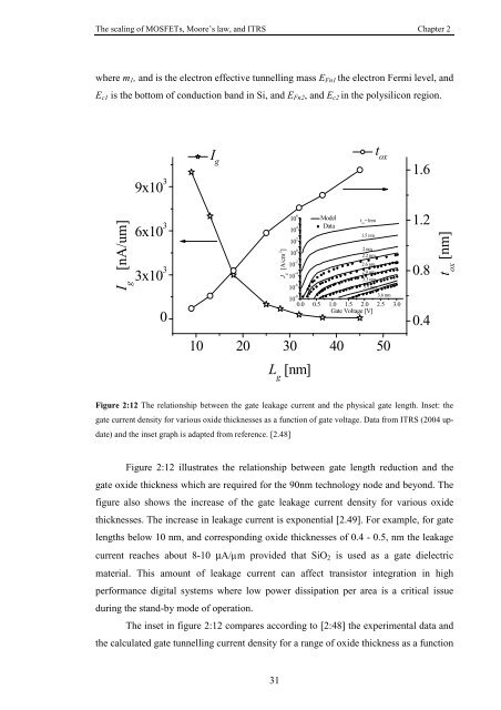
<strong>The</strong> <strong>scaling</strong> <strong>of</strong> <strong>MOSFETs</strong>, Moore’s <strong>law</strong>, <strong>and</strong> <strong>ITRS</strong> Chapter 2where m 1 , <strong>and</strong> is the electron effective tunnelling mass E Fn1 the electron Fermi level, <strong>and</strong>E c1 is the bottom <strong>of</strong> conduction b<strong>and</strong> in Si, <strong>and</strong> E Fn2 , <strong>and</strong> E c2 in the polysilicon region.I g0.0 0.5 1.0 1.5 2.0 2.5 3.0t ox1.69x10 3 0.4I g[nA/um]6x10 33x10 30J g[A/cm 2 ]10 6 Model t ox=1nm10 4 Data1.5 nm10 210 02 nm2.2 nm10 -22.6 nm10 -42.9 nm3.3 nm3.5 nm10 -610 -8Gate Voltage [V]3.6 nm10 20 30 40 50L g[nm]1.20.8t ox[nm]Figure 2:12 <strong>The</strong> relationship between the gate leakage current <strong>and</strong> the physical gate length. Inset: thegate current density for various oxide thicknesses as a function <strong>of</strong> gate voltage. Data from <strong>ITRS</strong> (2004 update)<strong>and</strong> the inset graph is adapted from reference. [2.48]Figure 2:12 illustrates the relationship between gate length reduction <strong>and</strong> thegate oxide thickness which are required for the 90nm technology node <strong>and</strong> beyond. <strong>The</strong>figure also shows the increase <strong>of</strong> the gate leakage current density for various oxidethicknesses. <strong>The</strong> increase in leakage current is exponential [2.49]. For example, for gatelengths below 10 nm, <strong>and</strong> corresponding oxide thicknesses <strong>of</strong> 0.4 - 0.5, nm the leakagecurrent reaches about 8-10 µA/µm provided that SiO 2 is used as a gate dielectricmaterial. This amount <strong>of</strong> leakage current can affect transistor integration in highperformance digital systems where low power dissipation per area is a critical issueduring the st<strong>and</strong>-by mode <strong>of</strong> operation.<strong>The</strong> inset in figure 2:12 compares according to [2:48] the experimental data <strong>and</strong>the calculated gate tunnelling current density for a range <strong>of</strong> oxide thickness as a function31


