FLEX CIRCUITS DESIGN GUIDE
Minco Flex Circuits Design Guide - BiS Sistem
Minco Flex Circuits Design Guide - BiS Sistem
- No tags were found...

Create successful ePaper yourself
Turn your PDF publications into a flip-book with our unique Google optimized e-Paper software.
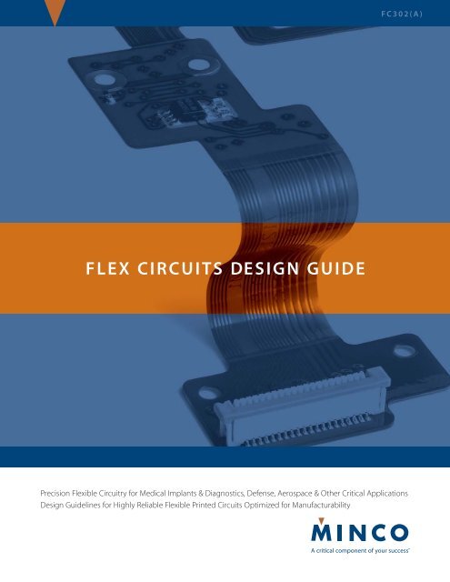
FC302(A)<br />
<strong>FLEX</strong> <strong>CIRCUITS</strong> <strong>DESIGN</strong> <strong>GUIDE</strong><br />
Precision Flexible Circuitry for Medical Implants & Diagnostics, Defense, Aerospace & Other Critical Applications<br />
Design Guidelines for Highly Reliable Flexible Printed Circuits Optimized for Manufacturability
Minco Flex Circuits<br />
Table of Contents<br />
Introduction: Click below to view pages<br />
How to Get Started . . . . . . . . . . . . . . . . . . . . . . . . . . . . . . . . . . . . . 3<br />
Benefits of Flex Circuits . . . . . . . . . . . . . . . . . . . . . . . . . . . . . . . . . 4<br />
High reliability<br />
Superior packaging solutions<br />
Design Options. . . . . . . . . . . . . . . . . . . . . . . . . . . . . . . . . . . . . . . . . 5<br />
Flex Circuit Design Process<br />
Design Guidelines . . . . . . . . . . . . . . . . . . . . . . . . . . . . . . . . . . . 6 - 9<br />
Specification documents<br />
Manufacturing a flex circuit<br />
Cost impact of layer count<br />
Circuit types<br />
Minco's General Capabilities . . . . . . . . . . . . . . . . . . . . . . . 10 - 13<br />
Standard specifications<br />
Testing<br />
Marking<br />
Controlling impedance and electrical noise<br />
Conductor width nomograph<br />
Standard Design Recommendations . . . . . . . . . . . . . . . . . 14 - 19<br />
Design differences and special considerations<br />
How to improve flexibility and bend radius<br />
Holes<br />
Tolerances<br />
Conductor width, thickness and spacing<br />
Materials<br />
Value Added Design Options . . . . . . . . . . . . . . . . . . . . . . 20 - 23<br />
Terminations<br />
Stiffeners<br />
Forming<br />
Population<br />
Custom and Integrated Components<br />
Request a Quote . . . . . . . . . . . . . . . . . . . . . . . . . . . . . . . . . . 24 - 26<br />
Providing information for a quote<br />
Specify testing requirements<br />
Artwork checklist<br />
Designing artworks<br />
CAD data guidelines<br />
Purpose of this Design Guide<br />
The purpose of this design guide is to enable you to design a highly<br />
reliable, flexible printed circuit optimized for manufacturability.<br />
While using this guide, keep in mind that the design information<br />
provided is only a suggestion. Minco takes pride in manufacturing<br />
flex circuits considered difficult to build. In most cases, we do<br />
build above and beyond the “standard” circuit specifications,<br />
provided that the circuit design and type allow for it.<br />
You are encouraged to contact Access: Minco Sales and Support<br />
at 763.571.3121 with your questions and concerns.<br />
Types of Flex circuits<br />
• Flex: Flexible version of Printed Circuit Board (PCB), with<br />
unique capabilities. Flex circuits offer the same advantages of<br />
a printed circuit board: repeatability, reliability, and high density<br />
but with the added “twist” of flexibility and vibration<br />
resistance. The most important attribute compelling designers<br />
to adopt flex circuit technology is the capability of the flex circuit<br />
to assume three-dimensional configurations.<br />
• Rigid-flex: A blend of rigid and flex emphasizing the best of<br />
both constructions, adding synergistic capabilities neither<br />
possess. In its most typical configuration, the rigid-flex is as a<br />
series of rigid PCBs joined by integrated flex circuits (with<br />
emphasis on the high percentage of rigid area content). There<br />
are many excellent possibilities for circuits designed primarily<br />
as a flex circuit with the addition of integrated rigid areas.<br />
Rigid areas provide excellent hard mount points for components,<br />
connectors and chassis while flex areas offer dynamic<br />
flexing, flex to fit, and component mounting poised to take<br />
advantage of these low mass and vibration resistant zones.<br />
This blending leads to creative solutions for your most<br />
demanding applications.<br />
• Flex-Coils: Custom wire-wound or etched coils may be<br />
integrated with any of our flex circuit or rigid-flex board types.<br />
Whether bonded to the surface or encapsulated in a high<br />
dielectric and abrasion resistant covering, these assemblies<br />
offer special capabilities to your coil designs.<br />
E2E — Engineer to Engineer . . . . . . . . . . . . . . . . . . . . . . . . . . . 27<br />
Early engineering involvement<br />
Ordering and delivery . . . . . . . . . . . . . . . . . . . . . . . . . . . . . . . . . 27<br />
Place your order with Minco<br />
Delivery information<br />
Glossary . . . . . . . . . . . . . . . . . . . . . . . . . . . . . . . . . . . . . . . . . . 28 - 30<br />
Next Steps . . . . . . . . . . . . . . . . . . . . . . . . . . . . . . . . . . . . . . . . . . . . 31<br />
2
How to Get Started<br />
1. Understand How Flex Circuits Work<br />
Carefully review the information in this guide and other<br />
online resources at www.minco.com/flex/. Knowledge of flex<br />
circuit types, capabilities and applications will provide the<br />
guidelines you need to design the best flex circuit for your<br />
product.<br />
2. Build a Flex Circuit Mock-up<br />
The dynamic nature of flex circuits allows for a multitude of<br />
design options. The best method for determining the validity<br />
of your design is to create a physical flex circuit mock up. To<br />
make your mock-up, follow these steps:<br />
a. Determine the system points to be electrically connected<br />
via flex circuitry and termination method(s) such as<br />
mating connectors, pins, ZIF, etc.<br />
b. Determine approximate circuit “footprint” that will provide<br />
conductor routing to each termination location.<br />
c. Review schematic or net list details along with special<br />
electrical requirements, such as plane layers, to determine<br />
approximate layer count.<br />
d. Examine sample circuits of similar layer counts to determine<br />
if proposed design will provide sufficient flexibility<br />
(you can order a Flex Circuit Design Kit, which contains<br />
circuit and material samples, at www.minco.com).<br />
e. Review mechanical requirements to ensure that bend<br />
radii fall within acceptable values for circuit thickness and<br />
layer count (refer to IPC-2223 for bend radius guidelines).<br />
f. Construct a “paper doll” outline of your flex circuit using<br />
heavy paper and check for fit. Make modifications as<br />
necessary. Continue constructing paper dolls and making<br />
modifications until the desired fit is achieved.<br />
g. Use .010" (0.25mm) polyester film to reconstruct the<br />
paper doll to make a representative mock-up. Install and<br />
make any dimensional adjustments as necessary.<br />
Your circuit outline is now complete and should be reconstructed<br />
in your CAD design software package. Using your<br />
circuit design software program, position connector footprints<br />
in the proper locations and route conductors per<br />
schematic or net list. Design rules for routing conductors on<br />
flexible circuits can be found in the IPC-2223 Sectional Design<br />
Standard for Flexible Printed Boards. You can also refer to the<br />
Standard Design Recommendations section in this guide.<br />
3. Obtain a Mechanical Sample<br />
Minco will review your design for possible improvements<br />
then propose building a mechanical sample using actual circuit<br />
stack-up materials. Before investing a lot of time and<br />
money to create a functional flex circuit prototype, testing a<br />
mechanical sample first ensures that your flex circuit has the<br />
right form and fit for your product. Form refers to the physical<br />
size, shape and mass of the part, while fit refers to its<br />
environmental interfaces, e.g. is it flexible enough to bend<br />
for installation, or will it meet temperature requirements? A<br />
mechanical sample helps you avoid installation problems or<br />
latent mechanical issues that could cause failures.<br />
To receive a flex circuit mechanical sample proposal:<br />
a. Construct a simple 2-dimensional CAD model consisting<br />
of the circuit outline and hole locations and sizes.<br />
b. Convert the CAD model to a 2-D DXF format and include<br />
a text file that provides the layer count, any special<br />
requirements, and a brief explanation of your application.<br />
Also include your name, company name, postal<br />
and email address, and phone number.<br />
c. Email this information to sales@minco.com.<br />
d. Minco will provide a response with a lead time for<br />
mechanical samples and advise if any charges are<br />
required.<br />
For More Information and Collaboration<br />
If you would like application or design engineering assistance,<br />
call Access: Minco Sales and Support at 763.571.3121 or visit us<br />
on the web at www.minco.com. You can also collaborate with<br />
other design engineers faced with creating their own prototype.<br />
On the Minco “E2E” Engineer to Engineer Discussion<br />
Board, a special forum has been created specifically for design<br />
engineers.<br />
Share your prototyping experiences, ask questions or help<br />
other design engineers looking for answers. Go to the E2E<br />
Community section on the Minco web site home page and<br />
click on the “Discussion Forum”. Choose the “Interconnectivity”<br />
forum, or enter this link in your browser address line:<br />
www.minco.com/community/forums/<br />
3
Benefits of Flex Circuits<br />
High reliability<br />
Repeatable installation<br />
Compared to discrete wiring, or ribbon cable, a flex circuit offers<br />
a customized repeatable routing path within your assembly. This<br />
gives you dependability where you need it. A flex circuit’s<br />
longevity can reduce service calls.<br />
Harsh environments<br />
Standard practice for flex boards is to cover the conductors with<br />
polyimide. This dielectric layer protects your circuits far beyond<br />
the capability of simple soldermask. Other base and cover<br />
materials are available for a broad range of ambient conditions.<br />
Long duty cycles<br />
By design, a flex circuit can be made very thin, yet robust<br />
enough to withstand thousands to millions of flexing cycles<br />
while carrying signal and power without a break.<br />
High vibration<br />
Under vibration and/or high acceleration, a flex circuit’s ductility<br />
and low mass will reduce the impact upon itself and solder<br />
joints. By contrast, a PCB’s higher vibrational mass will increase<br />
stresses upon itself, components and solder joints.<br />
Before: A tangle of wires connects<br />
four circuit boards.<br />
The flex circuit solution: A single circuit<br />
with 7 stiffeners and 2 connectors<br />
provides all the needed interconnects.<br />
After: The package is neat, lightweight, and less susceptible to connection<br />
failure.<br />
Superior packaging options<br />
Flex circuits can be shaped to fit where no other design can. They<br />
are a hybrid of ordinary printed circuit boards and round wire,<br />
exhibiting benefits of each. In essence, flex circuits give you unlimited<br />
freedom of packaging geometry while retaining the precision<br />
density and repeatability of printed circuits.<br />
Flex vs. wiring harness<br />
• Space and weight reduction: A single flex circuit can replace several<br />
hardboards, cables, and connectors.<br />
• Fast assembly: Flex circuits eliminate the need to color code and<br />
wrap bundles of wire, reducing the chance of assembly rejects<br />
and in-service failures. Total installed costs are lower, especially<br />
with volume production.<br />
• Repeatable wire routing: Eliminate wire routing errors; reducing<br />
test time, rework, and rejects<br />
• Robust connections: Flat foil conductors dissipate heat better, carrying<br />
more current than round wires of the same cross-sectional<br />
area. Conductor patterns in a flex circuit maintain uniform electrical<br />
characteristics. Noise, crosstalk, and impedance can be predicted<br />
and controlled.<br />
Flex vs. hard board (PCB)<br />
• Versatile shape: The most important attribute compelling designers<br />
adopt flex circuit technology is the capability of the flex circuit<br />
to assume three-dimensional configurations.<br />
• Lower mass: With a little experimentation and imagination, a flex<br />
circuit can save up to 75% of the space and/or weight of conventional<br />
wiring.<br />
• Vibration resistance: Recurring costs are lower than many wire<br />
harnesses, and since a flex circuit is more resistant to shock and<br />
vibrations than a PCB, repair and replacement costs are less.<br />
Rigid-flex<br />
• Double side component mounting: Rigid-flex are the ideal<br />
solution for flex circuits where surface mount components will<br />
be mounted on both sides of the board.<br />
• Total cost of ownership: The maximum benefit of rigid-flex is<br />
realized when the complete installation is reviewed for total<br />
cost of ownership. Using rigid-flex eliminates connections in<br />
the flex-to-rigid transitions while improving impedance control.<br />
• Most capable/Maximum vibration resistance: Lets you integrate<br />
the best capabilities of resistant rigid areas and resilient flex areas.<br />
• High mass component mounting: When mounting a high mass<br />
component, a rigid board is the right solution. A rigid-flex board<br />
gives you a smooth transition between rigid and flex areas while<br />
preserving the benefits of each.<br />
Flex-Coils<br />
• Custom coil winding: State of the art equipment generates a<br />
highly repeatable component<br />
• Integrated assembly: allows best packaging of your fragile coil in<br />
a flex circuit sub-assembly.<br />
4
Design Options<br />
Rigid-flex<br />
Hybrid hardboard/flex circuits can<br />
have up to sixteen layers. They replace<br />
bulky wire harnesses with compact,<br />
robust design.<br />
Pins<br />
Minco can braze or solder pins to<br />
circuits, either through holes or as<br />
extensions to conductors.<br />
Fine lines<br />
0.002" conductors and spaces are<br />
possible.<br />
Stiffeners<br />
An inexpensive alternative to rigid-flex.<br />
Connectors<br />
Built-in connectors speed your assembly.<br />
Optional epoxy potting seals<br />
between the circuit and connector.<br />
Shielding<br />
Solid or patterned shield planes reduce<br />
noise and control impedance of signal<br />
lines. Use matched impedance flex<br />
circuits for high-speed signal integrity.<br />
Wave solder carrier<br />
Stiffener material frames the circuit to<br />
hold it flat during wave solder. After<br />
soldering, just clip out and install.<br />
Factory forming<br />
Factory formed circuits<br />
follow tight curves to save space.<br />
Coils<br />
Minco’s unique flat wound inductive coils<br />
can be laminated into flex circuits.<br />
Applications include pacemaker antennas<br />
and eddy current generators.<br />
Surface mount<br />
Combine the space and weight savings<br />
of surface mounting with those of flex<br />
circuits for the ultimate in high-density<br />
packaging.<br />
Selective bonding<br />
For better flexibility along circuit arms,<br />
individual layers are unbonded and<br />
allowed to flex freely. Each layer has it’s<br />
own substrate and cover.<br />
Integrated solutions<br />
Minco integrates temperature sensors and<br />
etched-foil heaters with flex circuits for<br />
unified temperature control.<br />
5
Design Guidelines<br />
Specification documents:<br />
Consult standard specifications and design documents pertaining<br />
to your application and circuit requirements.<br />
IPC specifications*<br />
www.ipc.org<br />
• IPC-2221A, Generic Standard on Printed Board Design<br />
• IPC-2223, Sectional Design Standard for Flexible Printed<br />
Boards<br />
• IPC-4101, Specification for Base Materials for Rigid and<br />
Multilayer Printed Boards<br />
• IPC-4202, Flexible Base Dielectrics for Use in Flexible Printed<br />
Circuitry<br />
• IPC-4203, Adhesive Coated Dielectric Films for Use as Cover<br />
Sheets for Flexible Printed Circuitry and Flexible Adhesive<br />
Bonding Films<br />
• IPC-4204 Flexible Metal-Clad Dielectrics for Use in Fabrication<br />
of Flexible Printed Circuitry<br />
• IPC-6013, Qualification and Performance Specification for<br />
Flexible Printed Wiring<br />
• IPC-MF-150, Copper Foil for Printed Wiring Applications<br />
• IPC Position Paper: Transitioning from MIL-P-50884C and<br />
MIL-PRF-31032 to IPC-6013 and Amendment 1<br />
*For more information on IPC specifications, contact:<br />
IPC<br />
3000 Lakeside Drive, Suite 309 S<br />
Bannockburn, IL 60015-1249 USA<br />
Tel: 847.615.7100 / FAX: 847.615.7105<br />
URL: http://www.ipc.org<br />
Military www.dscc.dla.mil/Programs/MilSpec/DocSearch.asp<br />
• MIL-P-50884 (inactive for new designs), Printed Wiring, Flexible<br />
and Rigid-flex for Electronic Printed Wiring<br />
• MIL-PRF-31032/3A, Printed Wiring Board, Flexible, Single and<br />
Double Layer, With or Without Plated Holes, With or Without<br />
Stiffeners, for Soldered Part Mounting<br />
• MIL-PRF-31032/4A, Printed Wiring Board, Rigid-Flex or Flexible,<br />
Multilayer, with Plated Holes, with or Without Stiffeners, for<br />
Soldered Part Mounting<br />
IPC recommends that companies using MIL-PRF-31032<br />
specifications for printed circuits, alternatively specify that<br />
flexible circuits be supplied under IPC-6013 Class 3 performance<br />
requirements. Government agencies have generally<br />
accepted that this is a COTS (Commercial, Off-The-Shelf ) equivalent<br />
to MIL-PRF-31032. Please see the IPC position paper<br />
which is available for download at IPC.org or Minco.com.<br />
If your circuit must meet performance requirements of<br />
MIL-P-50884, MIL-PRF-31032 or IPC-6013, we urge you to read<br />
the IPC-2223 design specification for flexible circuits and follow<br />
its recommendations.<br />
Minco documents<br />
www.minco.com/flex/<br />
• Flex-Coils - Technical Specification FC01<br />
• Minco/Omnetics Flex Circuit Interconnect Solutions -<br />
Technical Specification FC04<br />
• Designing for Flexibility and Reliability - Application Aid<br />
FAA31<br />
6
Design Guidelines<br />
Manufacturing a flex circuit<br />
Building a flex circuit generally involves the same steps from circuit to circuit. However, certain circuit designs can add cost. For example,<br />
a single-layer circuit with access holes on both sides is more expensive than a single-layer circuit with access on one side, because<br />
the double-sided access hole circuit must have its substrate drilled separately. The flow chart and illustrations below identify some cost<br />
driven issues, such as access holes, plated through-holes, etc. The<br />
flow chart shows the manufacturing process for a standard<br />
double-layer circuit with a stiffener.<br />
Base<br />
Material<br />
Drill<br />
Plate Print Etch<br />
Copper<br />
Top<br />
Cover<br />
Drill<br />
Copper<br />
Polyimide<br />
Substrate<br />
Adhesive<br />
Plated<br />
Copper<br />
Bottom<br />
Cover<br />
Drill<br />
1. Double-sided material is drilled 2. Through-holes are copper-plated<br />
Adhesive<br />
Laminate<br />
Conductor<br />
FR-4<br />
Material<br />
Tack<br />
Drill<br />
Solder<br />
Pad<br />
3. Copper is etched to create<br />
conductors and pads<br />
Access Hole<br />
4. Polyimide covers are laminated<br />
over etched copper<br />
Ship<br />
Inspect<br />
Laminate<br />
Blank<br />
Cost impact of layer count<br />
The information for the chart (right) was taken from a sample of<br />
circuits built with Minco’s standard materials. This chart is not<br />
intended to be used as a price guide. However, it does show<br />
that circuit cost generally rises with layer count.<br />
It is in your best interest to consider all options to minimize<br />
cost. For example, use two circuits to do the job of one. Two<br />
double-layer circuits may be less expensive than one four-layer<br />
circuit. But the cost savings of the circuit may be offset by additional<br />
assembly requirements. Circuits can also be folded in<br />
order to save space and layers. Each situation is unique. A relatively<br />
small amount of time invested in project assessment can<br />
result in significant savings overall.<br />
COST MULTIPLIER<br />
6<br />
5<br />
4<br />
3<br />
2<br />
1<br />
0<br />
1-Layer<br />
Access<br />
1-Side<br />
1-Layer<br />
Access<br />
2-Sides<br />
2-Layer<br />
3-Layer<br />
Multi-Layer<br />
CIRCUIT TYPE<br />
4-Layer<br />
Multi-Layer<br />
4-Layer<br />
Rigid-Flex<br />
7
Design Guidelines<br />
Circuit types<br />
Single-layer<br />
• IPC 6013, MIL-P-50884 - Type 1<br />
• One conductive layer, either bonded between two insulating layers<br />
or uncovered on one side.<br />
• Access holes to conductors may be on either one or both sides.<br />
Access holes on both sides of a single-layer are more expensive since<br />
the substrate must be drilled or punched separately.<br />
• Stiffeners, pins, connectors, components, are optional.<br />
Access Hole<br />
Cover**<br />
Adhesive*<br />
Polyimide Substrate<br />
Copper Pad<br />
Double-layer<br />
• IPC 6013, MIL-P-50884 - Type 2<br />
• Two conductive layers with an insulating layer between; outer layers<br />
may have covers or exposed pads.<br />
• Plated through-holes provide connection between layers.<br />
• Access holes or exposed pads without covers may be on either or<br />
both sides; vias can be covered on both sides.<br />
• Stiffeners, pins, connectors, components are optional.<br />
Multilayer<br />
• IPC 6013, MIL-P-50884 - Type 3<br />
• Three or more flexible conductive layers with flexible insulating layers<br />
between each one; outer layers may have covers or exposed pads.<br />
• Plated through-holes provide connection between layers.<br />
• Access holes or exposed pads without covers may be on either or<br />
both sides.<br />
• Vias can be blind or buried.<br />
• Stiffeners, pins, connectors, components are optional.<br />
Multilayer, not plated through-holes<br />
• IPC 6013, MIL-P-50884 - Type 5<br />
• Two or more conductive layers with insulating layers<br />
between each one; outer layers may have covers or exposed<br />
pads.<br />
Access Hole<br />
Polyimide Cover<br />
Adhesive<br />
Copper Pad<br />
Polyimide Cover<br />
Copper-Plated<br />
Through-Hole<br />
Polyimide Substrate<br />
Access Hole<br />
Cover<br />
Copper Pad<br />
Polyimide Substrate<br />
Bond Ply<br />
Polyimide Substrate<br />
Adhesive<br />
Cover<br />
Copper-Plated Through-Hole<br />
Access Hole<br />
Cover**<br />
Adhesive*<br />
• Through-holes are not plated.<br />
• Access holes or exposed pads without covers may be on<br />
either or both sides.<br />
• Stiffeners, pins, and connectors are optional.<br />
Copper Pad (Layer #1)<br />
Cover**<br />
Copper Pad (Layer #2)<br />
** Adhesiveless base material also available<br />
**Cover may be replaced by photo-imagable coverlay (PIC)<br />
Polyimide Substrate<br />
8
Design Guidelines<br />
Circuit types<br />
Rigid-flex<br />
• IPC 6013, MIL-P-50884 - Type 4<br />
• Two or more conductive layers with either flexible or rigid insulation<br />
material as insulators between each one; outer layers may have<br />
covers or exposed pads.<br />
• Rigid-flex has conductors on the rigid layers, which<br />
differentiates it from multilayer circuits with stiffeners.<br />
Plated through-holes extend through both rigid and<br />
flexible layers (with the exception of blind and buried vias).<br />
Rigid-flex costs more than a standard circuit with stiffeners.<br />
• Access holes or exposed pads without covers may be on<br />
either or both sides. Vias or interconnects can be fully<br />
covered for maximum insulation.<br />
Adhesive<br />
Rigid Material<br />
Polyimide Cover<br />
Adhesive<br />
Polyimide Cover<br />
Polyimide Substrate<br />
Polyimide Substrate<br />
Copper Pad<br />
Copper-Plated Through-Hole<br />
• Stiffeners, pins, connectors, components, heat sinks, and mounting brackets are optional.<br />
• We also manufacture “flush” rigid-flex, where the top surface of contact areas is level<br />
with adjacent adhesive/insulation.<br />
• Minco is capable of sequentially laminating, drilling, and plating circuits, which allows<br />
for more flexibility in designing the circuit.<br />
Flex-Coils<br />
Flex-Coils are flex circuits containing integral wire coils<br />
for use as antennas or inductors. There are three basic<br />
types of Flex-Coils:<br />
• Simple, flat coils with wire leads<br />
• Coils laminated inside flex circuits<br />
• “Rim” coils that are built up in the Z-axis<br />
Wire Coil<br />
Etched Conductor<br />
Coil-to-Circuit<br />
Termination<br />
Flex-Coils have the same advantages that a flex circuit does. Wiring errors are reduced because the coil is oriented in the same spot<br />
every time, which provides repeatable signals. Flex-Coils are rugged and easy to assemble, and their design usually guarantees a<br />
reduced package size. A Flex-Coil can terminate in any manner that a flex circuit can, or to a wire lead. Heavy wire leads are available.<br />
See Flex-Coils Technical Specification FC01, for more information on Flex-Coil capabilities, design considerations, and the information<br />
required for a quote or build.<br />
Integrated solutions<br />
Minco is a leading manufacturer of temperature sensors and<br />
Thermofoil flexible heaters. We have the unique ability to integrate<br />
these components and a flex circuit into a single package, drastically<br />
reducing assembly time and potential errors. Call Access: Minco Sales<br />
and Support to discuss your application, or visit www.minco.com.<br />
** Adhesiveless base material also available<br />
9
Minco’s General Capabilities<br />
Standard specifications<br />
Physical properties<br />
Circuit size/standard panel size: 10.5 × 22" max./12 × 24",<br />
16.5 × 22" max./18 × 24", 267 x 559mm max./305 x 610mm,<br />
419 x 559mm max./457 x 610mm<br />
Layers: 16 maximum.<br />
Conductor width/space:<br />
0.0015” (0.038mm) minimum /0.0015” (0.038mm) minimum.<br />
Hole diameter (plated): 0.002” (0.051mm) minimum.<br />
Aspect ratio (ratio of hole depth/hole diameter):<br />
12:1 maximum.<br />
Outline dimensions and hole-to-border tolerance:<br />
SRD:<br />
0.015” (0.38mm) + 0.1% linear distance<br />
Laser/Hard tool: 0.003” (0.08mm) + 0.1% linear distance<br />
CMD:<br />
0.010” (0.25mm) + 0.1% linear distance<br />
Cluster-to-cluster tolerance:<br />
0.002” (0.05mm) + 0.1% linear distance<br />
Bend radius (flexibility):<br />
Single-layer: 6 × circuit thickness (minimum)<br />
Double-layer: 12 × circuit thickness (minimum)<br />
Multilayer: 24 × circuit thickness (minimum)<br />
Circuit thickness is approximately 0.006" (0.15mm) per layer.<br />
Sharper, permanent bends are common for bend-to-install<br />
applications. Call Access: Minco Sales and Support at<br />
763.571.3121 to ask about factory forming.<br />
Temperature: -65 to 150°C (-85 to 302°F).<br />
Will withstand a 5-second solder immersion at 260°C (500°F)<br />
without blistering, delaminating, or discoloring.<br />
Chemical resistance: No detrimental loss of physical properties<br />
when immersed for 15 minutes in acetone, methyl alcohol,<br />
toluene, or trichloroethylene.<br />
Materials<br />
Cover/substrate: Polyimide film: 1 mil (25μm)*, 2 mil (50μm)*,<br />
3 mil (75μm), 5 mil (125μm); Photoimageable Coverlay (PIC);<br />
Epoxy glass or polyimide glass (rigid-flex)<br />
Conductor:<br />
Copper: 1/8 oz. (5μm), 1/4 oz. (9μm), 1/3 oz. (12μm),<br />
1/2 oz. (18μm)*, 1 oz. (35μm)*, 2 oz. (71μm), 3 oz. (107μm)<br />
Cupronickel: 0.625 mil (15μm), 0.9 mil (22μm), 1.3 mil (33μm),<br />
1.9 mil (48μm), 2.3 mil (58μm)<br />
Nickel: 2 mil (50μm), 5 mil (125μm)<br />
Adhesive: Acrylic*, flame retardant, epoxy, epoxy prepreg,<br />
polyimide prepreg, phenolic<br />
Stiffener: Epoxy-glass (FR-4), polyimide-glass, polyimide, copper,<br />
aluminum.<br />
* These are the most common materials used for manufacturing flex circuits<br />
for maximum flexibility. See page 19 or contact Minco for materials not listed<br />
or special considerations (e.g. implantable devices, extended temperature<br />
range, etc.)<br />
10<br />
Surface finish (plating)<br />
Plating methods: Panel, selective, thruhole, blind via, buried via<br />
Plating materials: Solder, hard gold, soft gold, tin, nickel, electroless<br />
nickel with immersion gold (ENIG), OSP<br />
Electrical characteristics<br />
Insulation resistance: 100 MΩ minimum @ 25°C (77°F),<br />
assuming 0.010" (0.25mm) minimum conductor spacing.<br />
Dielectric (typical): 1000 VRMS @ 60 Hz for 30 seconds, 1 mA<br />
maximum leakage current.<br />
Shield layers: Solid or grid patterns; copper foil or screened<br />
conductive ink.<br />
Inductor/Antenna coils: Specify inductance (10 mH to 30 mH,<br />
typical). Wire-wound coils may be integrated into the circuit.<br />
The cover encapsulates the coil, conductors, and coil connections.<br />
For details, see Flex-Coils- Technical Specification FC01<br />
at www.minco.com/flex/.<br />
Heaters/Temperature sensors: Minco is a leading manufacturer<br />
of temperature sensors and Thermofoil flexible heaters. We<br />
have the unique ability to integrate these components and a<br />
flex circuit into a single package, drastically reducing assembly<br />
time and potential errors. Call Minco to discuss your application,<br />
or visit www.minco.com.<br />
Value added assemblies**<br />
Connectors:<br />
Clincher:<br />
0.100" (2.54mm) minimum, center-to-center;<br />
Micro series: 0.050" (1.27mm) minimum, center-to-center;<br />
Nano series: 0.025" (0.63mm) minimum, center-to-center.<br />
Optional epoxy potting is available.<br />
Fingers:<br />
Supported: 0.006" (0.15mm) minimum, center-to-center;<br />
Unsupported: 0.020" (0.50mm) minimum, center-to-center.<br />
In-line or right angle.<br />
Pins:<br />
Swaged/soldered: 0.085" (2.15mm) min., center-to-center;<br />
0.100" (2.54mm) typical;<br />
Brazed:<br />
0.035" (0.89mm) min., center-to-center.<br />
Active Components:<br />
Pick-and-place, Hand solder or braze<br />
Surface mount, through hole, embedded<br />
** See pages 20 – 22 for more information on incorporating these assemblies<br />
into your design.<br />
Quality management<br />
Minco is certified to ISO 9001: 2000 / AS/EN/SJAC9100<br />
quality system requirements<br />
All specifications subject to change.
Minco’s General Capabilities<br />
Testing<br />
When specifying testing, consider your needs carefully. Overspecification<br />
can greatly increase circuit cost. Minco encourages<br />
electrical testing. It is required on all multilayer, rigid-flex, and<br />
factory-formed circuits that are fabricated to MIL-P 50884, and<br />
certain classes of IPC-6013.<br />
See the table below for information on Minco’s test capabilities.<br />
Minco can test for… Range of operation<br />
IPC-6013<br />
N.A.<br />
MIL-P-50884 conformance<br />
Complete dimensions Resolution: 4 decimal places<br />
Accuracy: 0.001” (0.025mm) +<br />
0.008% of linear distance<br />
Dielectric withstanding Up to 6000 V<br />
Electrical continuity 1 Ω to 10 k Ω; suggest 5 Ω<br />
Stimulus: 0.01 V to 5.0 V<br />
Ionic cleanliness<br />
.5 microgram/square cm<br />
NACL equivalent<br />
Insulation resistance 10 k Ω to 100 M Ω at 10 V to 250 VDC<br />
Suggest 100 M Ω at 100 VDC<br />
Thermal shock -70 to 200°C<br />
Moisture resistance Up to 98% relative humidity<br />
Plating thickness<br />
Down to 0.000001" (0.02μm)<br />
Flexibility<br />
0 to 999,999 flexes<br />
Microsections Viewed at up to 1000×<br />
Marking<br />
Minco can meet your marking requirements.<br />
Our legend marking system offers silkscreen-like printing using<br />
a durable white ink that meets IPC-TM-650 industry standards.<br />
This system allows us to incorporate date code and serial numbering,<br />
along with panel based marking, at the same time.<br />
We can also offer traditional epoxy ink hand stamp or silkscreen<br />
printing if an alternate color or legacy specification is required.<br />
Etched marking within the part is also an option. Stiffeners and<br />
covers may be marked with component mounting locations.<br />
Controlling impedance and electrical noise<br />
Predictable electrical characteristics make flex circuits an ideal<br />
choice for high-speed signal transmission. Uniform spacing<br />
between conductors and grounds, continuous shield layers,<br />
and repeatable geometries are features that help control<br />
impedance and reduce crosstalk. And with flex circuits, you can<br />
eliminate connectors and other transitions that contribute to<br />
signal attenuation.<br />
Minco can provide tight tolerances on line width, spacing, and<br />
distance to ground layers in order to meet your impedance<br />
requirements. Actual impedance will also depend on the circuit’s<br />
shape after installation.<br />
Contact Minco for advice on designing circuits to specific<br />
electrical characteristics.<br />
• Microstrip - a single ground plane beneath the signal lines.<br />
Signal<br />
Ground<br />
• Stripline - dual ground layers above and below the signal<br />
lines.<br />
Ground<br />
Signal<br />
Ground<br />
• Edge coupled differential pairs – traces are adjacent to each<br />
other in the same plane with tightly controlled width and<br />
spacing, ground plane optional.<br />
Signal<br />
Ground<br />
• Rigid-flex/stiffened flex circuits with uninterrupted ground<br />
layers.<br />
• Silver epoxy coating. Silver epoxy is applied to the outside of<br />
circuits and electrically connected to other layers via access<br />
holes in the cover coat. Silver epoxy shielding is more flexible<br />
than copper.<br />
11
Minco’s General Capabilities<br />
Conductor width nomograph<br />
The nomograph on the facing page will help you determine the<br />
maximum allowable current capacity (in amperes) of a conductor.<br />
Reprinted from IPC-2221 (and MIL-STD-2118), the nomograph<br />
shows current for various conductor thicknesses, width,<br />
and temperature rises.<br />
Using the nomograph<br />
1. Locate the width of the conductor on the left side of the<br />
bottom chart.<br />
2. Move right horizontally, until you intersect the line of the<br />
appropriate conductor thickness. Move down vertically to<br />
the bottom of the chart to determine the cross-sectional area<br />
of the conductor.<br />
3. Move up vertically, until you intersect the line of the appropriate<br />
allowable temperature rise. This is the increase in temperature<br />
of the current-carrying conductor. Conductor temperature<br />
should not exceed 105°C. For example, if the ambient<br />
temperature might reach 80°C, the temperature rise<br />
above ambient of the conductor should be less than 25°C<br />
(105°C - 80°C). In this case use the 20°C curve.<br />
4. Move left horizontally to the left side of the chart to<br />
determine the maximum allowable current.<br />
Reverse the order of these steps to calculate required conductor<br />
width for a given current.<br />
Conductor aspect ratio<br />
For best producibility, design conductors to be at least five<br />
times as wide as they are thick. For example, with 2 oz. Copper<br />
(0.0028"/50μm) design the conductors to be 0.0140" (0.36mm)<br />
or wider. In tight situations Minco is successful in achieving<br />
2.5:1 ratio conductor widths.<br />
Conductor<br />
Width<br />
Assumptions<br />
1. The nomograph is valid only for conductors with a polyimide<br />
cover layer — not exposed conductors.<br />
2. The conductor thickness includes copper plating. Be aware<br />
that plating may add 0.0005" (13μm) to 0.0014" (36μm) of<br />
thickness. Selectively plated circuits do not have significant<br />
plating over conductors. The nomograph does not apply for<br />
plated metals other than copper.<br />
3. Derate current by 15% for conductor thicknesses greater<br />
than 3 oz. (0.0042”/75μm).<br />
4. The temperature rise curves only recognize heat generated<br />
by the conductor itself. Heat from power dissipating components<br />
or nearby conductors on other layers is not included.<br />
5. It is assumed that conductor coverage is relatively small;<br />
i.e. there is enough free space between conductors for lateral<br />
heat dissipation. Groups of closely spaced parallel conductors<br />
on the same layer can be treated as one large conductor.<br />
Add all the cross sectional areas together and all the currents<br />
together to determine the temperature rise.<br />
6. Current ratings are for still air environments. Forced air cooling<br />
will increase the maximum allowable current. Operating<br />
circuits in a vacuum will greatly decrease the maximum<br />
allowable current.<br />
Contact Minco for assistance in cases where the nomograph<br />
does not apply. Also contact us if you have difficulty designing<br />
sufficient current capacity into the space available. We can suggest<br />
ideas to increase current capacity.<br />
T<br />
Adhesive<br />
Polyimide<br />
Ideal: Conductor width greater<br />
than 5x conductor thickness.<br />
12
Minco’s General Capabilities<br />
Conductor width nomograph<br />
Example #1: A current of 1 amp with ½ oz. copper and 30°C<br />
temperature rise will require a conductor width of 0.040”.<br />
Example #2: A 0.140" wide conductor etched from 1 oz. copper<br />
(0.0014") will produce a temperature rise of 10°C at 2.7 amp.<br />
17.5<br />
Wire Gauge Equivalent (AWG)<br />
34 32 30 28 26 24 22<br />
Conductor Width in Inches Current in Amperes<br />
15.0<br />
45°C<br />
12.5<br />
30°C<br />
10.0<br />
20°C<br />
7.5<br />
10°C<br />
6.0<br />
5.0<br />
4.0<br />
3.5<br />
3.0<br />
2.5<br />
2.0<br />
1.5<br />
1.0<br />
0.75<br />
0.50<br />
0.37<br />
0.25<br />
0.125<br />
0.062<br />
0<br />
0<br />
0.001<br />
0.005<br />
0.010<br />
0.015<br />
0.020<br />
0.030<br />
0.050<br />
Example #1<br />
0.070<br />
0.100<br />
3 Oz/ft2 (0.0042")<br />
0.150<br />
Example #2<br />
0.200<br />
2 Oz/ft2 (0.0028")<br />
0.250<br />
0.300<br />
½ Oz/ft2 (0.0007") 1 Oz/ft2 (0.0014")<br />
0.350<br />
0.400 0 1 5 10 20 30 50 70 100 150 200 250 300 350 400 450 500 600 700<br />
Cross Section Area in Square Mils<br />
Note: square mil = 6.4516x10^-4 square millimeter<br />
13
Standard Design Recommendations<br />
Design differences and special considerations<br />
Define circuit parameters by application<br />
It may be helpful to use a paper template to represent the circuit.<br />
Experiment with bending and forming the template to optimize<br />
shape and fit. When designing the final shape, consider how the<br />
circuits will lay out on a processing panel (“nesting”). The greater<br />
the number of circuits per panel, the lower the cost.<br />
Another consideration concerns rigid-flex. While Minco is capable<br />
of building a traditional rigid-flex board for you it may not<br />
be your best choice. Multilayer or stiffened flex boards may be<br />
able to meet your requirements for component and board<br />
mounting at reduced cost.<br />
Flex circuit vs. hardboards<br />
Designing a flex circuit is only one step away from designing a<br />
hardboard. The most important design difference to keep in mind<br />
is the three-dimensionality of a flex circuit. Creative bending and<br />
flexing can save space and layers. Other important differences:<br />
• Flex circuits both require and permit looser tolerances than<br />
hardboards.<br />
• Because arms can flex, design them slightly longer than<br />
required.<br />
Design tips to minimize circuit cost<br />
• Consider how circuits will be “nested” on a panel.<br />
Special considerations for rigid-flex<br />
• Rigid-flex is the ideal solution for applications with multiple<br />
rigid PCBs having SMT components on both sides and requiring<br />
interconnects between the rigid PCBs.<br />
• Before designing a rigid-flex circuit, make certain that it is<br />
truly what you need. If the circuit only has a few layers, stiffeners<br />
are a less expensive alternative to rigid-flex.<br />
• It is most cost effective to build a rigid-flex with an even number<br />
of layers. All rigid portions of the circuit should have the<br />
same number and stack-up of layers.<br />
• Observe aspect ratio (hole depth/hole diameter) limits (see<br />
Capabilities on page 10).<br />
• Minco builds circuits up to 16 layers, but costs increase significantly<br />
above 10 layers.<br />
• Expect a trim tolerance similar to that of a steel rule die from<br />
hole-to-border and border-to-border. Hole placement within a<br />
cluster of holes and from cluster-to-cluster will have a ±0.005"<br />
(0.13mm) tolerance within a single rigid area.<br />
• Minimum inside corner radius of 0.031" (0.79mm) is standard,<br />
but smaller radii are available.<br />
• Unbonded layers can increase flexibility in multilayer flex circuits,<br />
but this option is more expensive. Specify unbonded<br />
layers only in areas of the circuit that will bend.<br />
vs.<br />
• Minco can provide an epoxy fillet on stiffener edges that will<br />
bend or flex.<br />
Bend<br />
Bend<br />
• For rigid-flex circuits, it is less expensive to have plated<br />
through-holes in the rigid portions only.<br />
• Minco can provide blind and buried vias in rigid-flex circuits.<br />
Desired<br />
Circuit<br />
• Keep circuits small; consider using a set of smaller circuits<br />
instead of one large circuit.<br />
• Follow recommended tolerances whenever possible.<br />
• Design unbonded areas only where they are absolutely<br />
necessary.<br />
• If circuits have only a few layers, using stiffeners can be far less<br />
expensive than a rigid-flex circuit.<br />
14
Standard Design Recommendations<br />
How to improve flexibility and bend radius<br />
Single-layer circuits are the best choice for dynamic (flex-in-use)<br />
applications. Two or more layer circuits are best suited to static<br />
applications, with flexes only during installation.<br />
Several problems can arise when a circuit is bent sharply.<br />
Compression can cause wrinkles in the cover coat on the inside<br />
of the bend. Stretching can result in tears in the cover material<br />
and/or broken conductors on the outside of the bend.<br />
Start the mechanical design by establishing the bend radius. If<br />
the radius is at least ten times the thickness of the material,<br />
there is a good chance that the circuit will function reliably.<br />
The minimum allowable bend radius depends on a number of<br />
factors, and is best defined by IPC-2223. Overall circuit thickness<br />
is slightly less than the sum of the individual insulator,<br />
adhesive and foil layer thicknesses.<br />
Bend radius (flexibility):<br />
Single-layer: 6 × circuit thickness (minimum)<br />
Double-layer: 12 × circuit thickness (minimum)<br />
Multilayer: 24 × circuit thickness (minimum)<br />
Circuit thickness is approximately 0.006" (0.150mm) per layer.<br />
Incorporate these features into multilayer and reduced bend ratio designs to increase reliability<br />
1. Reduce overall thickness in the flex area<br />
• Reduce the base copper weight (and the corresponding adhesive<br />
thicknesses) or reduce the dielectric thickness.<br />
• Use adhesiveless base materials. Adhesiveless materials will<br />
usually reduce the starting thickness of each substrate by 1-2<br />
mils (25-50μm) when compared to adhesive based substrates.<br />
• Eliminate copper plating on the conductors in the flexing area<br />
by utilizing selective (pads-only) plating or adding outer padsonly<br />
layers to the circuit.<br />
2. Make the circuit robust to withstand flexing<br />
• Balance the conductor weights and material thicknesses on<br />
each side of the neutral bend axis.<br />
• Conductors should be staggered from layer to layer and not<br />
stacked on top of each other to increase flexibility.<br />
GOOD<br />
VS.<br />
BAD<br />
• Conductors should always be routed through bend areas as<br />
close to perpendicular as possible.<br />
• Incorporate tear stops or<br />
reliefs for slits in the circuit.<br />
The end of the slit represents<br />
a vulnerable point for a tear<br />
to start and to propagate.<br />
• Avoid any discontinuities in the cover coat or substrate near a<br />
bend.<br />
• The circuit outline should be designed so there are no twists<br />
in the finished assembly. Any burr or irregularity from the<br />
blanking operation could potentially propagate into a tear.<br />
• Consider factory forming. Reliable bend radii tighter than 10:1<br />
are possible if the circuit is formed using specialized tooling<br />
and will only be flexed one time.<br />
• If bend reliability is still a concern, consider "unbonding" the<br />
flexible substrates from each other. Since each of the substrates<br />
in the unbonded area has a much lower thickness than<br />
the total circuit, they are able to bend tighter than if they<br />
were fully bonded.<br />
For a more in-depth look at this subject please see<br />
Designing for Flexibility and Reliability<br />
Application Aid FAA31 - at www.minco.com/flex/<br />
• Conductor thickness and width should remain constant in<br />
bend areas.<br />
• Plated through holes should be kept out of the bend areas.<br />
• If the circuit will be bent within 1" (25.4mm) of termination<br />
pads, fillets should be placed at each conductor/pad interface.<br />
Stresses from a bend are not isolated to the immediate bend<br />
area and residual stresses can radiate out from the bend. See<br />
page 17 for more information on fillets.<br />
• If shields and/or ground planes are required on the circuit, use<br />
a crosshatched pattern rather than solid copper. Another<br />
shielding option is a screened-on conductive coating such as<br />
silver epoxy, which is much more flexible than copper.<br />
15
Standard Design Recommendations<br />
Holes<br />
General requirements for pads, access holes<br />
and annular rings<br />
Feature Single-layer Double-layer Multilayer<br />
Pad* 0.060" (1.5mm) + t 0.030" (0.76mm) + t Outer pad:<br />
0.030" (0.76mm) + t<br />
Inner pad:<br />
0.025" (0.63mm) + t<br />
Major 0.050" (1.3mm) + t 0.030" (0.76mm) + t 0.030" (0.76mm) + t<br />
access<br />
hole*<br />
Minor 0.015" (0.38mm) + t 0.015" (0.38mm) + t 0.015" (0.38mm) + t<br />
access<br />
hole‡<br />
t = nominal through-hole diameter.<br />
Vias<br />
Minco can provide circuits with covers that have no<br />
access holes exposing the vias (called 'tented vias').<br />
Minco can also provide blind and buried vias in multilayer<br />
and rigid-flex circuits. Blind vias connect the top<br />
or bottom conductor layer to adjoining layers, but the<br />
via does not extend through all layers. A buried via<br />
only connects internal layers and is not exposed in the<br />
finished circuit. Blind and buried vias increase circuit<br />
cost, but they free up space for additional conductors<br />
on the non-drilled layers.<br />
Tented Via<br />
Blind Via<br />
* Pad and major access hole design requirements are based on typical<br />
annular ring requirements of 0.015" (0.38mm) minimum for a single-layer,<br />
0.005" (0.13mm) minimum for all external layers, and 0.002" (0.05mm) minimum<br />
for multilayer innerlayers.<br />
‡ Customer must allow tangency (see the Glossary for a definition of<br />
tangency).<br />
For more information on access holes (major and minor) annular ring, pads,<br />
and thruholes, see the Glossary on pages 28 – 30.<br />
Access Hole<br />
Annular<br />
Ring<br />
Through-Hole<br />
Major<br />
Access Hole<br />
Buried Via<br />
Thruhole or Through-hole<br />
Plated through-holes (PTH) connect together the top, bottom,<br />
and any required internal conductor layers. PTHs are drilled<br />
oversize to accommodate the thickness of the copper plating<br />
that will cover the entire barrel of the hole as well as the surface<br />
of the outer pads. Exterior pads may be plated along with the<br />
entire foil surface or selectively plated just at the PTH site.<br />
Outer Pad<br />
Through Hole<br />
Inner Pad<br />
16<br />
Plated<br />
Wiring<br />
Hole<br />
Minor<br />
Access Hole<br />
Stiffener holes<br />
Stiffener holes should be a minimum of 0.015" (0.38mm) in<br />
diameter larger than the access hole. It is better if the access<br />
hole underneath the stiffener hole is a minor access hole in<br />
order to increase the stiffener web between holes and to<br />
prevent potential solder wicking between the stiffener and the<br />
circuit. The customer must allow tangency. Round stiffener holes<br />
are less expensive than slotted stiffener holes, and as mentioned<br />
before, thinner stiffener material (less than 0.031"/0.79mm) is<br />
less expensive to process.
Standard Design Recommendations<br />
Holes<br />
Wiring holes<br />
Minco can drill through-holes as small as 0.0039" (0.10mm). A<br />
0.020" (0.50mm) through-hole size is typical. Standard finished<br />
hole tolerance is ±0.003" (0.08mm). For all circuits, the finished<br />
through-hole size should be 0.003" (0.08mm) to 0.010"<br />
(0.25mm) larger in diameter than the component lead. This<br />
depends on the number of leads per component, and the positional<br />
tolerance of the component leads.<br />
Surface mount access<br />
Minco can provide flex circuits with areas that are specifically<br />
designed for surface mount components. Because covers are<br />
drilled, not silk-screened, round access holes are easier to provide.<br />
Square access holes will add to cost because the pad access area<br />
would have to be punched out with a punch-and-die. Square<br />
pads with round access holes are a good compromise. Below are<br />
some ideas for configuring pads for surface mount.<br />
It is best to specify round<br />
(instead of slotted), throughholes.<br />
This will reduce drilling<br />
time and cost.<br />
Access Hole<br />
Access Hole<br />
Leads<br />
Pads<br />
Whenever possible, design pads larger than the access holes. If<br />
space is critial, use hold-down tabs. Hold-down tabs are especially<br />
important for single-layer circuits, because a single-layer<br />
circuit does not have the added strength of plated throughholes.<br />
A variety of hold-down tab designs are available.<br />
Photoimageable coverlay materials are also available, and can<br />
provide intricate, irregular shaped openings for dense surface<br />
mount patterns.<br />
Soldering tips<br />
• Since polyimide absorbs moisture, circuits must be baked (1<br />
hour @ 120°C) before soldering.<br />
• Pads located in large conductor areas, such<br />
as ground planes, voltage planes, or heat<br />
sinks, should be provided with relief areas,<br />
as illustrated. This limits heat dissipation for<br />
easier soldering.<br />
Thermal relief<br />
• When hand soldering pins in dense clusters, try not to solder<br />
adjacent pins one after another. Move around to avoid local<br />
overheating.<br />
Pad fillets<br />
Pad fIllets improve etched yield and material strength. Fillets<br />
are appropriate when the pad diameter is greater than the connecting<br />
strand width. Acute angles at the interface between conductors<br />
and pads are to be avoided by using fillets to minimize the<br />
concentration of stress at the interface.<br />
Before fillets<br />
After fillets<br />
• Minco can solder connectors or components (SMT or Thruhole)<br />
as an added service.<br />
• Minco can supply circuits in panel form for easier component<br />
assembly.<br />
17
Standard Design Recommendations<br />
Tolerances<br />
You are not limited to the tolerances listed in this section. Tighter tolerances are achievable, but often at a higher cost. Accordingly,<br />
more relaxed tolerances will typically cost less. Even with relaxed tolerances, a flex circuit will have a uniformity that is impossible to<br />
attain with conventional wiring. The flexibility of materials constructing a flex circuit allow it to be more compliant than rigid circuits, so<br />
it is not always necessary to specify tight tolerances across all dimensions.<br />
Trimming<br />
Each trimming method has advantages and disadvantages. Routing and laser trimming provide hard tooling (punch and die) tolerances<br />
for small quantities of circuits. Laser trimming is also capable of complex cutouts not feasible with other methods. Steel rule dies<br />
(SRD) are best for intermediate quantities and tolerances. Chemical milled dies (CMD) offer tighter tolerances than SRDs for an incremental<br />
increase in cost. Hard tooling (punch and die) is recommended for tight tolerances, complex circuits, and/or high quantity. For<br />
more specific information on SRD, punch-and-dies and CMD, see the Glossary at the end of this guide.<br />
Circuit<br />
Outline dimensions (profile tolerance) Hole-to-border dimensions Cluster to<br />
dimension in<br />
inches(mm)†<br />
SRD CMD Punch and<br />
die /laser<br />
SRD CMD Punch and<br />
die /laser<br />
cluster§<br />
1 ±0.015 (0.38) ±0.010 (0.25) ±0.003 (0.08) ±0.015 (0.38) ±0.010 (0.25) ±0.007 (0.18) ±0.003 (0.08)<br />
5 ±0.020 (0.50) ±0.015 (0.38) ±0.007 (0.18) ±0.020 (0.50) ±0.015 (0.38) ±0.012 (0.30) ±0.007 (0.18)<br />
10 ±0.025 (0.63) ±0.020 (0.50) ±0.012 (0.30) ±0.025 (0.63) ±0.020 (0.50) ±0.017 (0.43) ±0.012 (0.30)<br />
15 ±0.030 (0.76) ±0.025 (0.63) ±0.017 (0.43) ±0.030 (0.76) ±0.025 (0.63) ±0.022 (0.55) ±0.017 (0.43)<br />
20 ±0.035 (0.88) ±0.030 (0.76) ±0.022 (0.55) ±0.035 (0.88) ±0.030 (0.76) ±0.027 (0.69) ±0.022 (0.55)<br />
† Round circuit to next highest increment.<br />
§ Represents from a group of holes to a group of holes. Holes within a group will have a tolerance of ±0.003" (0.08mm).<br />
Note: Dimensional tolerances are given in inches. See Glossary for definition of profile tolerance.<br />
Solder thickness<br />
Minco follows IPC-6013 requirements of coverage and solderability for solder coatings.<br />
Conductor width, thickness, and spacing<br />
See the nomograph on pages 12 – 13 for calculating the necessary conductor width and spacing. Minco can provide a 0.004" (0.10mm)<br />
minimum conductor width/spacing (0.0025"/0.063mm minimum at higher cost) on 1 oz. (25μm) copper and 0.005" (0.13mm) minimum<br />
conductor width-spacing on 2 oz. (50μm) copper (for thicker copper, consult Minco). For best producibility, design circuit conductors at<br />
least five times wider than they are thick.<br />
Tolerances for conductor width depend on whether the copper is plated or unplated.<br />
Copper thickness Plated copper Unplated copper<br />
½ oz. ±0.001" (25μm) ±0.001" (25μm)<br />
1 oz. ±0.002" (50μm) ±0.001" (25μm)<br />
2 oz. ±0.003" (75μm) ±0.002" (50μm)<br />
3 oz. ±0.004" (100μm) ±0.003" (75μm)<br />
18
Standard Design Recommendations<br />
Materials<br />
This table lists the materials and material thicknesses that Minco has available.<br />
Minco’s standard materials are in boldface. If the material or thickness is not listed, consult Minco at 763.571.3121.<br />
Material function Material type Sizes/thickness available<br />
Flexible insulator Kapton* and other polyimide films † 1/2 mil (12.5μm), 1 mil (25μm), 2 mil (50μm), 3<br />
mil (75μm), 5 mil (125μm)<br />
Rigid substrate (rigid-flex) FR-4 Variety of thicknesses between 0.003" (0.08mm)<br />
and 0.125" (3.18mm)<br />
Polyimide<br />
Variety of thicknesses between 0.003" (0.08mm)<br />
and 0.125" (3.18mm)<br />
Conductor Copper 1/4 oz. (9μm), 1/3 oz. (12μm), 1/2 oz. (18μm), 1 oz.<br />
(35μm), 2 oz. (71μm), 3 oz. (107μm), 5 oz.<br />
(175μm), 7 oz. (254μm), 10 oz. (356μm)<br />
Different forms of copper<br />
Half-hard, rolled-annealed, electro-deposited<br />
Beryllium copper<br />
3 mil (75μm): half-hard and quarter-hard<br />
4 mil (100μm): half-hard<br />
Cupro-nickel (70/30 alloy)<br />
0.625 mil (15μm), 0.9 mil (22μm), 1.3 mil (33μm),<br />
1.9 mil (48μm), 2.3 mil (58μm)<br />
Nickel<br />
2 mil (50μm), 3 mil (75μm), 5 mil (125μm)<br />
Silver epoxy ‡<br />
Adhesive § Modified acrylic 1/2 mil (12.5μm), 1 mil (25μm), 2 mil (50μm), 3<br />
mil (75μm), 4 mil (100μm)<br />
Modified epoxy<br />
1/2 mil (12.5μm), 1 mil (25μm), 2 mil (50μm), 3 mil<br />
(75μm), 4 mil (100μm)<br />
Phenolic Butyral<br />
1 mil (25μm)<br />
Pressure-sensitive adhesive (PSA)<br />
1 mil (25μm), 2 mil (50μm), 5 mil (125μm)<br />
Pre-impregnated material: FR-4, polyimide 2 mil (50μm), 8 mil (200μm)<br />
Stiffener Copper, Aluminum, and other metals Variety of thicknesses available<br />
Polyimide glass<br />
FR-4<br />
See “Rigid substrate/Polyimide glass” above<br />
Variety of thicknesses between 0.005" (0.13mm)<br />
and 0.125" (3.18mm)<br />
Polyimide 1/2 mil (12.5μm), 1 mil (25μm), 2 mil (50μm), 3<br />
mil (75μm), 5 mil (125μm)<br />
* Kapton is a registered trademark of DuPont for polyimide. Dielectric strength of plain Kapton film is 3500-7000 volts/mil (0.025mm) depending upon material<br />
thickness. Kapton/modified acrylic has a dielectric strength of 3500 volts/mil (0.025mm) and a temperature rating of -65 to 150°C, although circuits will discolor<br />
after long-term exposure at 150°C. For special applications, Minco can use an adhesive that will withstand temperatures of 150°C continuous, and<br />
200°C short-term.<br />
† Other polyimide films are available for special applications.<br />
‡ Material is applied as an alternative to standard copper layers.<br />
§ In general, Minco recommends 0.001" (25μm) of adhesive on the cover material per 1 oz. (35μm) of copper (including plated copper). There may be special circumstances<br />
where more is required. Consult Minco for details.<br />
19
Value Added Design Options<br />
Terminations<br />
There are a variety of terminations for a flex circuit, and a variety<br />
of methods for applying these terminations.<br />
Connectors<br />
Connectors are usually customer selected, but Minco can recommend<br />
certain types of connectors to meet specific application<br />
requirements. Connectors can be attached to flex circuits<br />
by hand soldering, wave soldering, crimping, or simple insertion<br />
with zero insertion force (ZIF) models. Connectors can be<br />
potted after attachment or conformally coated for protection<br />
and insulation with epoxy, polyurethane, or RTV.<br />
One good option for many low cost<br />
applications is the Clincher insulation<br />
displacement connector.<br />
High density connectors, with 0.050" (1.27mm) or 0.025"<br />
(0.63mm) center-to-center terminals, are available from Omnetics<br />
Connector Corporation in several forms, including high temperature<br />
and MIL-spec options.<br />
Finger type<br />
Supported<br />
Unsupported<br />
Pins<br />
Centerline distance<br />
0.006" (0.15mm) min.<br />
0.020" (0.51mm) min.<br />
• Socket pins are pressed in place and then soldered. Pins can<br />
be swaged to the circuit and soldered after the swaging procedure,<br />
or pins can be swaged to an FR-4 stiffener and then<br />
soldered. Swaged/soldered pins are moderately priced and<br />
have good mechanical strength.<br />
• End pins that are in line with conductors can be brazed, soldered,<br />
or crimped to conductors. Pins can be bent to form a<br />
staggered arrangement.<br />
• Flex circuits can interface to hardboards via soldered lap<br />
joints, lap joints applied with an anisotropic adhesive (conductive<br />
in the Z-axis only).<br />
Pins can be inserted separately or ganged in a header. Minco<br />
recommends using an FR-4 or polyimide stiffener in pin areas to<br />
improve mechanical strength and simplify assembly.<br />
Pin type Centerline distance<br />
Swaged 0.100" (2.54mm) typical, 0.085" (2.15mm) min.<br />
Brazed 0.100" (2.54mm) typical, 0.035" (0.89mm) min.<br />
Vertical or horizontal mounting<br />
to fit your designs.<br />
Up to 44 Beryllium Copper<br />
pins in less than half the<br />
space of an 0.050"(1.27mm)<br />
connector!<br />
Mil-spec connectors with<br />
temperature ratings to 200°C.<br />
Round form connectors for<br />
surface mount installation.<br />
Crimped sockets and pins<br />
Connector type<br />
Clincher connector<br />
Micro series pin center-to-center<br />
Nano series pin center-to-center<br />
Centerline distance<br />
0.100" (2.54mm) min.<br />
0.050" (1.27mm) min.<br />
0.025" (0.63mm) min.<br />
Swaged or nailhead pins<br />
with stiffener<br />
Fingers<br />
Fingers can be supported or unsupported. Supported fingers<br />
are ideal for ZIF connectors mounted on rigid boards.<br />
Unsupported fingers can be hot bar soldered to hard circuit<br />
boards.<br />
End pins<br />
Lap joint<br />
Supported fingers<br />
Unsupported fingers<br />
20
Value Added Design Options<br />
Stiffeners<br />
Benefits of using a stiffener<br />
• Stiffeners are an inexpensive option for rigidizing pin areas,<br />
surface mount areas, or hole patterns for component mounting<br />
(provided SMT components are on one side only). Surface<br />
mount areas do not always require a stiffener, depending on<br />
component size, but a stiffener is recommended and will add<br />
very little to cost or bulk.<br />
• Stiffeners can be utilized to force a bend line in selected<br />
areas. Minco can provide epoxy fillets for the edges of the<br />
FR-4 stiffener, where flexing occurs.<br />
• Stiffeners reinforce solder joints and increase abrasion<br />
resistance.<br />
• Circuits may be attached to a stiffener pallet (multiple parts)<br />
to provide easier handling for automated pick-and-place and<br />
component soldering. Circuits can be held together for processing<br />
on the pallet, then singulated (clipped free) after<br />
wave soldering and circuit testing.<br />
• Stiffeners can be silk-screened with component mounting<br />
locations for rapid assembly.<br />
• Stiffeners are commonly FR-4 or polyimide material. They are<br />
usually applied with modified acrylic adhesive.<br />
• Standard FR-4 material thicknesses range from 0.003"<br />
(0.08mm) to 0.125" (3.18mm). Typical thickness for polyimide<br />
stiffeners is 0.005" (125μm), but 0.001" (25μm), 0.002" (50μm),<br />
and 0.003" (75μm) are also available. Polyimide stiffeners are<br />
less expensive than FR-4 stiffeners because they are punched<br />
on a die instead of routed with a drill bit. The polyimide stiffener<br />
lay-up procedure is performed with alignment pins,<br />
therefore, registration is better. The polyimide stiffeners are<br />
trimmed with the cover on the final blanking procedure,<br />
which guarantees perfect outside alignment.<br />
• When using multiple stiffeners, maintaining the same<br />
stiffener thickness consistent throughout the entire construction<br />
will help keep costs under control.<br />
21
Value Added Design Options<br />
Forming<br />
Flexible materials don’t guarantee that the circuit will function<br />
reliably when bent or flexed. There are many factors that contribute<br />
to the reliability of a printed flex circuit and all of these<br />
factors must be taken into account during the design process<br />
to ensure that the finished circuit will function reliably.<br />
When designing a flex circuit, the designer must factor in all of<br />
the parameters that will have an impact on the circuit’s ability<br />
to bend or flex in the specific application. These include, but are<br />
not limited to: whether the application is static or dynamic,<br />
bend radii, dielectric thicknesses and type, foil weight, copper<br />
plating, overall circuit thickness, number of layers, and number<br />
of flexures.<br />
The tighter a bend radius becomes, the higher the probability<br />
of failure during flexing. Keeping the overall thickness of the<br />
flex circuit in a bend area to its minimum will increase reliability.<br />
The ratio of bend radius to thickness is one indicator of whether<br />
the design is going to be reliable or have a high probability of<br />
failure. If the bend radius is at least ten times the thickness of<br />
the material, there is a good chance that the circuit will function<br />
reliably. If the calculated bend radius falls below ten to one,<br />
the design may be questionable. Formulas for calculating the<br />
minimum allowable bend radius for several circuit types can be<br />
found in IPC-2223.<br />
It is possible to design for much tighter bend radii, in a bendto-install<br />
application which retains the formed shape of the circuit.<br />
The circuit must be designed to withstand stretching along<br />
the outer bend and compression of materials on the inner<br />
bend. Stretching can tear covers or crack conductors while<br />
compression causes foil and cover wrinkling that can also lead<br />
to tears. These problems become more of a concern in applications<br />
that require the circuit to be bent beyond a 90-degree<br />
angle. As the bend angle increases beyond 90 degrees, the<br />
damaging effects of stretching and compressing increase dramatically.<br />
Any time that a reduced radii bend beyond 90<br />
degrees is incorporated into a circuit design, the circuit should<br />
be bent one time only. On bends over 90 degrees, it is also<br />
advisable to constrain the circuit in the formed condition to<br />
keep it from relaxing or being inadvertently reopened.<br />
The ideal circuit design would have no copper plating on the<br />
conductors in the forming or flexing area. Electrolytic copper<br />
has much lower ductility than that of rolled annealed copper,<br />
making it much more susceptible to fracturing when it is bent<br />
or flexed. Other types of plating, such as gold and/or nickel,<br />
should be avoided in the flexing area for the same reasons.<br />
Copper plating on the flexing conductors may be eliminated by<br />
using pads-only plating or designing with pads-only layers on<br />
the external surfaces.<br />
Minco can factory form some flex circuits with radii all the way<br />
down to a “crease”, dependent upon board design, to improve<br />
installation precision and repeatability within our customer’s<br />
assembly process.<br />
When designing a part for forming, it is important to avoid<br />
mechanical stressors in the bend zone. Stressors include pads,<br />
holes, components, and sharply angled conductors. These<br />
reflect the most common features problematic to forming.<br />
Forming imparts stress into circuits. Some designs will be better<br />
suited to this forming process than others. Minco encourages<br />
customers to discuss the intended usage of parts they want<br />
formed with our engineers to help determine suitability.<br />
Forms are likely to relax slightly over time. Tightly toleranced<br />
forms are not normally held by flex circuits. Minco recommends<br />
specifications to read “reference only” or to describe the<br />
parts as “capable of attaining ‘x’ dimensions” for both angular<br />
and linear aspects of forming.<br />
Formed parts are less capable of withstanding temperature<br />
variations than their un-formed counterparts. This is particularly<br />
true where the bend zones are exposed to solder reflow or high<br />
temperature sterilization procedures. To work around these limitations<br />
Minco can suggest optional designs or assembly<br />
processes. Please contact us to discuss your needs.<br />
Population<br />
Minco will also assemble hardware and electronic components<br />
onto your flex and rigid-flex circuits.<br />
Numerous connectors are available for flex termination, ranging<br />
from crimp connectors to nano-size SMT connectors or discrete<br />
pins.<br />
Heat-sinks, metal stiffeners, and plastic mounting frames may<br />
also be laminated, heat staked or glued to flex circuits.<br />
Flex-coil designs are an example of an embedded component<br />
supplied within flex, multilayer, and rigid-flex circuits.<br />
The most common electronic components are typically surface<br />
mounted to the flex circuit using automated pick-and-place<br />
equipment. Design considerations for populating flex circuits<br />
differ slightly from rigid boards. Simple flex circuits usually need<br />
to be stiffened for surface mount components. Our design engineers<br />
will make recommendations for necessary design factors<br />
to meet your needs.<br />
Between our in-house capabilities and our vendor network<br />
we’re able to offer our customers bare parts, palletized and<br />
unpopulated, partially populated or fully populated.<br />
22
Value Added Design Options<br />
Custom and Integrated Components<br />
Dependable component customization and integration from the people who made the components<br />
dependable in the first place.<br />
Minco operates four different product divisions, all coordinated in the same facility for faster, seamless integration that can boost your<br />
time-to-market. This makes us unique in our ability to customize and integrate components into turnkey assemblies and complete<br />
thermal, sensing and flex circuitry solutions. All of our components can be designed, manufactured, and integrated to perfectly fit your<br />
application while providing matched system accuracy.<br />
Custom Solutions<br />
Minco's customized products provide an affordable solution to meet your exact specifications. We work diligently to build our products<br />
with the greatest efficiency, quality, and accuracy to meet your critical standards and ensure ROI.<br />
Minco can customize all of our products to perfectly fit your application.<br />
Thermofoil Heaters<br />
• Irregular shapes, size and holes for a precise fit<br />
• Single or dual element for critical redundancy and rapid heat transfer<br />
• Profiled and multi-zone heaters to put the heat exactly where you need it<br />
• Leadwire, flex circuit or solder pad terminations for easy integration into your assembly<br />
Sensors and Instruments<br />
• RTD and thermistor elements to match any TCR (temperature coefficient of resistance) curve<br />
• A variety a materials and machining options available to provide critical<br />
thermal response in your application<br />
• Leadwire and cable options to meet your application parameters<br />
• Custom transmitters, controllers, and monitors for accurate sensing packages<br />
Flex Circuits<br />
• Single sided, double sided, multilayer and rigid-flex circuits with high layer counts to meet your<br />
interconnection needs<br />
• Fine lines, circuit forming and selective bonding add to space and weight savings<br />
• Stiffeners, pins, connectors and full turnkey electronics packaging for efficient integration<br />
into your application<br />
• Inductive communication coils can be integrated with flex circuits to provide critical communication assemblies<br />
Integrated Solutions<br />
All of Minco’s products – Thermofoil Heaters, Flex Circuits, Sensors, Instruments – can be integrated into a single component for<br />
greater efficiency. Whether it is a complete thermal optimization system or interconnection application, Minco’s design engineers will<br />
partner with you to ensure success.<br />
With integrated solutions there is less work on your end, and less that can go wrong. Our integrated<br />
assemblies truly lower your total cost of ownership (TCO) because of less front end assembly, easy<br />
installation, and unparalleled quality and reliability.<br />
23
Request a Quote<br />
Providing information for a quote<br />
Information required for a ballpark quote<br />
• Quantity desired<br />
• Number of layers<br />
• General size of the circuit<br />
• Features such as stiffeners, pins, connectors, etc.<br />
Information required for a firm quote<br />
• Drawing (Gerber data preferred)<br />
• Quantity required<br />
• Complete physical shape<br />
• Materials: conductors, insulators, stiffeners, other<br />
• Number of layers<br />
• Plating requirements<br />
• Applicable specifications<br />
• Unusual areas of the circuit that Minco should be aware of,<br />
such as unbonded or cut-away areas<br />
• Tolerances clearly outlined (geometric profile preferred)<br />
• Other requirements: conductor spacing, conductor width,<br />
border, etc.<br />
• Special marking and/or packaging requirements<br />
• Testing requirements: type, percent to be tested, and frequency.<br />
Is IPC-6013 testing required?<br />
• Additional components that Minco is expected to<br />
supply/assemble (inform Minco of preferred suppliers if the<br />
components are unique)<br />
Information required for manufacturing<br />
All the information that is required for a firm quote, plus:<br />
• Dimensional drawing including notes and requirements<br />
• Artwork for conductors in digital format, coupons, and<br />
screened marking, if applicable (unless Minco is to generate)<br />
Supplying drawings<br />
The “perfect drawing” will provide the following information:<br />
• Cross-section diagram (i.e. material stack-up)<br />
• Outline drawing of circuit<br />
• Material listing<br />
• Specifications<br />
• Hole chart<br />
• Feature chart (i.e. minimum conductor width and spacing, and<br />
any other minimum spacing requirements)<br />
• Dimensional tolerances<br />
• Special plating requirements<br />
• Marking requirements<br />
• Testing requirements<br />
• Special packaging requirements<br />
For more information call Access: Minco Sales and Support at<br />
763.571.3121<br />
Specify testing requirements<br />
Testing is labor intensive and will directly impact costs and<br />
delivery schedules. Some tests are automated, others are manual.<br />
Test frequency must be considered as well as the destructive<br />
nature of some tests. All tests are documented and certificates<br />
of conformance are routine for Minco.<br />
Test requirements must be documented to avoid any confusion.<br />
Your sales and design engineer contacts can discuss these<br />
needs with you.<br />
Physical testing options include, but are not limited to<br />
• Dimensional measurements<br />
• Ionic contamination<br />
• Thermal shock<br />
• Solderability<br />
Electrical testing options include, but are not limited to<br />
• Resistance<br />
• Insulation resistance (IR)<br />
• Continuity<br />
• Inductance<br />
• Capacitance<br />
• Sencore Ringer<br />
• Dielectric, net-to-net<br />
• Dielectric, high potential test of exterior insulation<br />
• Impedance<br />
Note: Standard electrical testing includes continuity (5 Ω ) and insulation<br />
resistance (40 mΩ @ 150 VDC).<br />
24
Request a Quote<br />
Artwork checklist<br />
Minco strongly encourages customers to use the artwork<br />
checklist provided. If you answer 'yes' to all the criteria, your artwork<br />
will probably not need adjustment.<br />
Note: Depending on the size/complexity of the circuit, the criteria may<br />
differ.<br />
Dimensions<br />
• Does the border match the print dimensionally?<br />
• Does the artwork match the print dimensionally?<br />
Etched marking (if any)<br />
• Are all features of letters and symbols at least 0.010" (0.25mm)<br />
wide?<br />
• Are letters and symbols clear of conductors and borders?<br />
Border and cutouts<br />
• Is there a trim border (part outline) on at least one layer?<br />
• Do nominal borders allow for tolerances in the table on page 10?<br />
Non-wiring hole clearance<br />
• Are non-wiring holes at least 0.007" (0.18mm) (more preferred)<br />
over the specified minimum distance from conductors<br />
and borders?<br />
Conductor width<br />
Is artwork conductor width:<br />
• at least 0.001" (25μm) over the specified minimum for<br />
unplated 1/2 oz. (18μm) Copper?<br />
• at least 0.004" (100μm) over the specified minimum for<br />
unplated 1 oz. (35μm) (or thicker) copper?<br />
• at least 0.005" (125μm) over the specified minimum for plated<br />
copper?<br />
Conductor spacing<br />
Is artwork conductor space:<br />
• at least 0.001" (25μm) over the specified minimum for all<br />
unplated copper?<br />
• at least 0.002" (50μm) over the specified minimum for all<br />
plated copper?<br />
Conductor routing<br />
• Are conductors perpendicular to bend lines?<br />
• Have you avoided the I-beam effect? (See page 15 or Glossary<br />
for a definition of I-beam effect)<br />
Pads and annular rings<br />
• Are there pads on all layers for all plated through-holes?<br />
• Are non-exposed pads (via pads) 0.020" (0.51mm) larger than<br />
the through-holes (not applicable for micro vias)?<br />
• Are center locations provided for all drilled holes and/or slots?<br />
• Are the annular rings on all holes at .east 0.007" (0.18mm)<br />
larger than the specified minimum?<br />
• Are access holes in cover layers at least 0.007" (0.18mm)<br />
(more preferred) over the specified minimum distance from<br />
conductors and borders?<br />
• Are all pads filleted?<br />
25
Request a Quote<br />
Designing CAD artworks<br />
This section provides the information necessary for designing<br />
CAD artworks that will meet the tolerance and quality requirements<br />
for a flex circuit. A correctly designed artwork will prevent<br />
unnecessary and costly delays in the initial shipment.<br />
Most CAD artwork is customer supplied. Minco can generate<br />
CAD artworks at additional cost. To generate an artwork, Minco<br />
needs:<br />
• Locations where the circuit will be bent, if any, and required<br />
flexibility at these locations (i.e. bending for installation or a<br />
dynamic application).<br />
• We prefer that you supply CAD generated data. If you cannot<br />
furnish CAD data, we can digitize a physical artwork at additional<br />
cost.<br />
• Outline dimensions and tolerances. See Page 18.<br />
• Location and size of conductor pads. See the table on page 16.<br />
• Minimum conductor widths, minimum spaces between conductors<br />
and conductor thickness. These will depend on current carrying<br />
capacity, impedance, dielectric, and the flexibility requirements<br />
of the circuit. See the nomograph on pages 12 – 13.<br />
• Net list<br />
• Conductor paths can be captured from a net list or schematic<br />
when required. A design charge may apply.<br />
CAD-generated artwork<br />
CAD data guidelines<br />
Minco can accept CAD data in the following forms<br />
• Gerber RS-274X format (embedded aperture) photoplotter<br />
code is preferred.<br />
• RS-274D Gerber data with separate, detailed aperture list can<br />
be used, but is not preferred.<br />
• AutoCAD DXF (2D)<br />
• AutoCAD DWG (2D)<br />
Other formats may be acceptable — contact Minco for details.<br />
Transferring data to Minco<br />
You can transfer your media to Minco in the following forms,<br />
which are listed in order of preference.<br />
• E-mail: Contact Access: Minco Sales and Support at<br />
763.571.3121<br />
• FTP: Contact Access: Minco Sales and Support at 763.571.3121<br />
• Floppy (3.5"), Zip disk, or CD: IBM-PC format<br />
Guidelines for all formats<br />
• Single entity draws for conductors are required.<br />
Guidelines for DXF<br />
• Place artwork data, part outline, hole centers, soldermask,<br />
coverlay, screen marking, etc. on separate, individual CAD system<br />
layers.<br />
• Polygons or zero width line draws for irregular pad shapes and<br />
shield area outlines are preferred (instead of filling in these<br />
shapes).<br />
• Supply arcs and circles. Do not convert arcs or circles into segmented<br />
lines.<br />
• Avoid supplying only conductor outlines, as it increases set-up<br />
cost. If you do supply conductor outlines, include supporting<br />
CAD system layer with proper line width conductors and pads.<br />
Guidelines for Gerber<br />
When sending your photoplotter code, please include:<br />
• The format of the data<br />
• An aperture wheel listing (when required)<br />
• A list of layers with descriptions<br />
• The number of files supplied<br />
• Single pad flashes are required.<br />
• Minimize the entities used to create conductor to pad transitions<br />
(“fillets”).<br />
26
E2E — Engineer to Engineer<br />
Early engineering involvement<br />
Great flex designs are achieved when the designer understands<br />
that flexible circuits are as much a mechanical component as<br />
they are electrical. Engineering consultation can be invaluable<br />
early in the design process. Minco wants to make your access to<br />
engineering tools and expertise as convenient as possible.<br />
That is why we have developed an E2E (engineer to engineer)<br />
community online at www.minco.com/e2e.<br />
Circuit design assistance is available with online resources,<br />
including an "Ask the Experts" link to request help from Minco<br />
experts and an "E2E Community Discussion Forum" where<br />
questions may be posted to the engineering community<br />
beyond Minco.<br />
Minco engineer review<br />
Our engineers will review your quote or order documentation<br />
and data to determine if changes are needed for manufacturability.<br />
If needed, we will discuss these issues with you to our<br />
mutual agreement before construction begins.<br />
Design services<br />
Start to finish or problem specific, design engineers are available<br />
to assist our customers. Access: Minco Sales and Support<br />
(763.571.3121) will put you in contact with the design engineer<br />
most able to help you with your specific design.<br />
Ordering and Delivery<br />
Place your order with Minco<br />
When you receive your Minco quote you will possibly see an<br />
itemized list of comments regarding your circuit. Please thoroughly<br />
review your Minco quote. Placement of an order<br />
includes acceptance of all terms, conditions, exceptions and<br />
substitutions. Our sales professionals are happy to discuss any<br />
questions you have regarding your Minco quote.<br />
When placing your order, include final design data, drawings,<br />
and procurement documentation reflecting your expectations<br />
and Minco’s DFM changes. Clarity is key to Minco’s relationships<br />
with customers.<br />
All quality clauses and expectations should be detailed during<br />
the RFQ/Quote stage.<br />
Delivery information<br />
Call Access: Minco Sales and Support at 763.571.3121 for estimated<br />
ship dates. Lead times may vary depending on design and<br />
work flow requirements.<br />
Production models will follow our best practices and applicable<br />
lead times. Delivery times and quality are predictable for all<br />
standard designs.<br />
Prototype/quick-turn models are generally offered on a "best<br />
effort" basis with regard to meeting all print requirements. We<br />
can also provide many designs completely "per print". Minco’s<br />
quick-turn group offers fast proof of concept constructions that<br />
may uncover improvements as well as road-blocks.<br />
Send your purchase order and all other required information to<br />
Access: Minco Sales and Support (763.571.3121).<br />
27
Glossary<br />
Access hole<br />
A hole in the cover layer of a circuit that allows electrical access<br />
to a flex circuit’s conductor pads and through-holes.<br />
Conductor width<br />
The width of a conductor measured across its base.<br />
Conductor<br />
Width<br />
Annular ring<br />
The ring of exposed copper or solder that surrounds a flex<br />
circuit’s through-holes.<br />
Annular<br />
Ring<br />
Access Hole<br />
Artwork<br />
The original pattern of conductor strands for a flexible circuit.<br />
Chemically milled die (CMD)<br />
A tool used in a punch press with blades formed by a chemical<br />
milling process, and mounted on a 1" (2.54cm) thick aluminum<br />
base.<br />
Conductor<br />
The path that carries electrical current from one point to another.<br />
Minco’s flex circuit conductors are commonly found in the form<br />
of copper strands.<br />
Conductor<br />
Adhesive<br />
Polyimide<br />
Cover<br />
Insulator material laminated to an etched element. Covers can<br />
be located on the inner or outer layers. Internal cover layers are<br />
found in the unbonded regions of a circuit.<br />
Dynamic application<br />
The use of a flex circuit in an environment that requires flexing<br />
in use.<br />
Flex circuit<br />
Flexible printed circuits made from etched foil conductor<br />
strands. The conductor strands are laminated between insulating<br />
layers. Flex circuits can vary in complexity from the simplest<br />
single-layer circuit to a complex multilayer.<br />
Flex-Coil<br />
Flex circuits with internal or attached wire-wound coils.<br />
Hold-down tabs<br />
An extension of foil on a conductor pad that aids the pad in<br />
gripping to the substrate insulation. Hold-down tabs are also<br />
referred to as “anchoring spurs.”<br />
Hold-Down<br />
Tab<br />
Conductor spacing<br />
The width of space between conductor strands. A certain minimum<br />
conductor spacing must exist in order to prevent conductors<br />
from shorting together.<br />
Conductor<br />
Spacing<br />
I-beam effect<br />
The tendency of a flex circuit to have reduced flexibility and<br />
fracture conductor strands if the conductor strands are layered<br />
directly over each other, instead of being staggered from layer<br />
to layer.<br />
Adhesive<br />
Polyimide<br />
28
Glossary<br />
Impedance<br />
The measurement in ohms of the apparent resistance of an AC<br />
circuit. Impedance depends on several factors: DC resistance,<br />
capacitance, inductance of the line, the width of the conductor<br />
strands, and the conductor spacing relative to ground and insulating<br />
layers.<br />
Major access hole<br />
An access hole (see “Access hole”) that is large enough to<br />
expose a major portion of a conductor pad, which is usually<br />
coated with solder.<br />
Major<br />
Access Hole<br />
Minor access hole<br />
An access hole (see “Access hole”) that exposes only a very small<br />
portion of a conductor pad, used on holes where a solder pad is<br />
not needed or desired. The cover hole must still be larger than<br />
the through-hole to allow for normal registration tolerances.<br />
Minor<br />
Access Hole<br />
Pad<br />
The portion of a conductor, usually surrounding a through-hole,<br />
that is used to connect a component for an electrical connection.<br />
Pads are sometimes referred to as “terminals” or “lands.”<br />
Profile tolerance<br />
Dimensional tolerancing where the part trim line is contained<br />
within a tolerance zone consisting of the area between two parallel<br />
lines, separated by the specified tolerance. For example, a<br />
circuit to be trimmed with a steel rule die might have a tolerance<br />
of 0.015" (0.38mm) (A 0.030"/0.76mm wide profile tolerance<br />
zone). The circuit trim line could vary anywhere inside the<br />
zone.<br />
A<br />
Pad<br />
DRAWING CALLOUT<br />
.030" (0.76mm) A B<br />
B<br />
NOMINAL TRIM LINE<br />
Nesting<br />
Designing circuits so that they lay closely together on a panel<br />
during production. This maximizes the usage of panel space,<br />
which minimizes production cost.<br />
EXAMPLE<br />
.030" (0.76mm) WIDE<br />
TOLERANCE ZONE<br />
Punch-and-die<br />
Hard-tooling that is used in a punch press. A punch-and-die<br />
consists of two precisely matched metal plates held in special<br />
die shoes. When the punch press is activated, the plates come<br />
together in order to punch a specific pattern into material.<br />
29
Glossary<br />
Rigid-flex<br />
A circuit containing both rigid and flexible areas. The rigid layers<br />
have conductors and plated through-holes connecting<br />
them to other layers.<br />
Selective plating<br />
A method of plating flex circuits so that only the circuit’s<br />
through-holes and surrounding pads are plated. This greatly<br />
adds to a circuit’s flexibility.<br />
Static application<br />
The use of a flex circuit in an environment that requires flexing<br />
during installation and maintenance, but not in operation.<br />
Steel rule die (SRD)<br />
A tool used in a punch press, consisting of steel cutting blades<br />
in a pattern, embedded into a maple plywood base.<br />
Tear stops<br />
Copper, polyimide, or Teflon guards that are located in the inner<br />
corners of polyimide-insulated flex circuits in order to prevent<br />
propagation of tears.<br />
Through-holes<br />
Holes that are drilled through the layers of a flex circuit in order<br />
to have component access to those layers. Connection from<br />
one layer to the next is provided by plating the through-hole<br />
walls with a thin layer of copper.<br />
Trim line<br />
The area defined by a design engineer as the final cut-out area<br />
around a flex circuit.<br />
Trim Line<br />
Stiffener<br />
Flexible or rigid pieces of material (usually polyimide or FR-4)<br />
added to flex circuits to reinforce them for component mounting.<br />
There are no conductors on stiffeners, as compared to rigidflex<br />
circuits.<br />
Substrate<br />
A layer of insulator bonded on one or both sides with foil.<br />
Unbonded areas<br />
A flex circuit design technique that involves providing an insulating<br />
layer between every conductive layer of a flex circuit, but<br />
with no adhesive bonding between the insulating layers in certain<br />
areas of the circuit. This technique improves circuit flexibility.<br />
Via<br />
A plated through-hole with no cover access holes that provides<br />
connection for internal layers.<br />
Tangency<br />
A condition that occurs when the edge of a stiffener or cover<br />
access hole is flush with the edge of a through-hole.<br />
Through-Hole<br />
Stiffener<br />
30
Next Steps<br />
Minco welcomes the opportunity to help you design and manufacture a product<br />
that meets or exceeds your expectations. That is why we have established a<br />
variety of communication channels so that we may encourage meaningful<br />
exchange and dialog.<br />
Call Access: Minco Sales and Support – 763.571.3121<br />
The Access: Minco Sales and Support team is trained and equipped to promptly handle complex questions regarding<br />
product orders, quote requests, engineering questions, and other issues that require comprehensive customer support.<br />
Get a mechanical sample of your flex circuit<br />
Take advantage of Minco’s offer to build a flex circuit mechanical sample that will help you avoid installation problems or<br />
mechanical issues that could cause failures. Follow the instructions provided in the "How to Get Started" section of this<br />
guide.<br />
Collaborate with other engineers<br />
Engineers are being asked to provide input on an increasingly broader number of disciplines. That’s why more of them<br />
are finding value in collaborating with other engineers. Share your prototyping experiences, ask questions or help other<br />
design engineers looking for answers. Go to the E2E Community section on the Minco web site home page and click on<br />
the “Discussion Forum”. Choose the “Interconnectivity” forum, or enter this link in your browser address line:<br />
www.minco.com/community/forums/<br />
Submit a request for quote – www.minco.com/rfq/<br />
Send us your application specifications and component needs, and a Minco Representative will contact you by phone or<br />
email to confirm your request and will send you a reliable quotation.<br />
31
Worldwide Headquarters<br />
7300 Commerce Lane<br />
Minneapolis, MN 55432 USA<br />
Tel: 1.763.571.3121<br />
Fax: 1.763.571.0927<br />
sales@minco.com<br />
www.minco.com<br />
European Headquarters<br />
Usine et Service<br />
Commercial, Z.I.<br />
09310 Aston, France<br />
Tel: (33) 5 61 03 24 01<br />
Fax: (33) 5 61 03 24 09<br />
Asia Pacific Headquarters<br />
20 Science Park Road<br />
#02-31 Teletech Park<br />
Singapore Science Park II<br />
Singapore 117674<br />
Tel: (65) 6511 3388<br />
Fax: (65) 6511 3399<br />
ISO 9001:2000<br />
FC302060906(A)<br />
© Minco 2007<br />
Flex Circuits<br />
Thermofoil Heaters<br />
Sensors<br />
Instruments