FLEX CIRCUITS DESIGN GUIDE
Minco Flex Circuits Design Guide - BiS Sistem
Minco Flex Circuits Design Guide - BiS Sistem
- No tags were found...

Create successful ePaper yourself
Turn your PDF publications into a flip-book with our unique Google optimized e-Paper software.
Standard Design Recommendations<br />
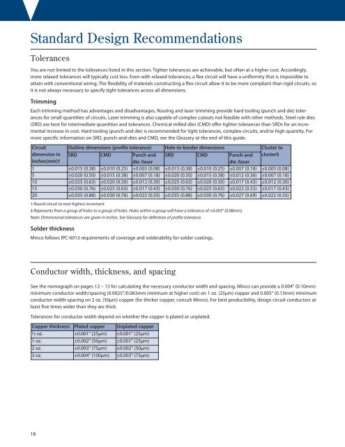
Tolerances<br />
You are not limited to the tolerances listed in this section. Tighter tolerances are achievable, but often at a higher cost. Accordingly,<br />
more relaxed tolerances will typically cost less. Even with relaxed tolerances, a flex circuit will have a uniformity that is impossible to<br />
attain with conventional wiring. The flexibility of materials constructing a flex circuit allow it to be more compliant than rigid circuits, so<br />
it is not always necessary to specify tight tolerances across all dimensions.<br />
Trimming<br />
Each trimming method has advantages and disadvantages. Routing and laser trimming provide hard tooling (punch and die) tolerances<br />
for small quantities of circuits. Laser trimming is also capable of complex cutouts not feasible with other methods. Steel rule dies<br />
(SRD) are best for intermediate quantities and tolerances. Chemical milled dies (CMD) offer tighter tolerances than SRDs for an incremental<br />
increase in cost. Hard tooling (punch and die) is recommended for tight tolerances, complex circuits, and/or high quantity. For<br />
more specific information on SRD, punch-and-dies and CMD, see the Glossary at the end of this guide.<br />
Circuit<br />
Outline dimensions (profile tolerance) Hole-to-border dimensions Cluster to<br />
dimension in<br />
inches(mm)†<br />
SRD CMD Punch and<br />
die /laser<br />
SRD CMD Punch and<br />
die /laser<br />
cluster§<br />
1 ±0.015 (0.38) ±0.010 (0.25) ±0.003 (0.08) ±0.015 (0.38) ±0.010 (0.25) ±0.007 (0.18) ±0.003 (0.08)<br />
5 ±0.020 (0.50) ±0.015 (0.38) ±0.007 (0.18) ±0.020 (0.50) ±0.015 (0.38) ±0.012 (0.30) ±0.007 (0.18)<br />
10 ±0.025 (0.63) ±0.020 (0.50) ±0.012 (0.30) ±0.025 (0.63) ±0.020 (0.50) ±0.017 (0.43) ±0.012 (0.30)<br />
15 ±0.030 (0.76) ±0.025 (0.63) ±0.017 (0.43) ±0.030 (0.76) ±0.025 (0.63) ±0.022 (0.55) ±0.017 (0.43)<br />
20 ±0.035 (0.88) ±0.030 (0.76) ±0.022 (0.55) ±0.035 (0.88) ±0.030 (0.76) ±0.027 (0.69) ±0.022 (0.55)<br />
† Round circuit to next highest increment.<br />
§ Represents from a group of holes to a group of holes. Holes within a group will have a tolerance of ±0.003" (0.08mm).<br />
Note: Dimensional tolerances are given in inches. See Glossary for definition of profile tolerance.<br />
Solder thickness<br />
Minco follows IPC-6013 requirements of coverage and solderability for solder coatings.<br />
Conductor width, thickness, and spacing<br />
See the nomograph on pages 12 – 13 for calculating the necessary conductor width and spacing. Minco can provide a 0.004" (0.10mm)<br />
minimum conductor width/spacing (0.0025"/0.063mm minimum at higher cost) on 1 oz. (25μm) copper and 0.005" (0.13mm) minimum<br />
conductor width-spacing on 2 oz. (50μm) copper (for thicker copper, consult Minco). For best producibility, design circuit conductors at<br />
least five times wider than they are thick.<br />
Tolerances for conductor width depend on whether the copper is plated or unplated.<br />
Copper thickness Plated copper Unplated copper<br />
½ oz. ±0.001" (25μm) ±0.001" (25μm)<br />
1 oz. ±0.002" (50μm) ±0.001" (25μm)<br />
2 oz. ±0.003" (75μm) ±0.002" (50μm)<br />
3 oz. ±0.004" (100μm) ±0.003" (75μm)<br />
18