FLEX CIRCUITS DESIGN GUIDE
Minco Flex Circuits Design Guide - BiS Sistem
Minco Flex Circuits Design Guide - BiS Sistem
- No tags were found...

Create successful ePaper yourself
Turn your PDF publications into a flip-book with our unique Google optimized e-Paper software.
Standard Design Recommendations<br />
Holes<br />
Wiring holes<br />
Minco can drill through-holes as small as 0.0039" (0.10mm). A<br />
0.020" (0.50mm) through-hole size is typical. Standard finished<br />
hole tolerance is ±0.003" (0.08mm). For all circuits, the finished<br />
through-hole size should be 0.003" (0.08mm) to 0.010"<br />
(0.25mm) larger in diameter than the component lead. This<br />
depends on the number of leads per component, and the positional<br />
tolerance of the component leads.<br />
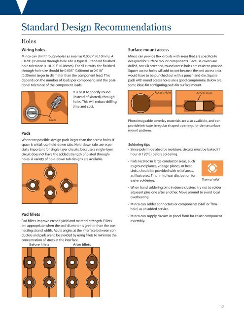
Surface mount access<br />
Minco can provide flex circuits with areas that are specifically<br />
designed for surface mount components. Because covers are<br />
drilled, not silk-screened, round access holes are easier to provide.<br />
Square access holes will add to cost because the pad access area<br />
would have to be punched out with a punch-and-die. Square<br />
pads with round access holes are a good compromise. Below are<br />
some ideas for configuring pads for surface mount.<br />
It is best to specify round<br />
(instead of slotted), throughholes.<br />
This will reduce drilling<br />
time and cost.<br />
Access Hole<br />
Access Hole<br />
Leads<br />
Pads<br />
Whenever possible, design pads larger than the access holes. If<br />
space is critial, use hold-down tabs. Hold-down tabs are especially<br />
important for single-layer circuits, because a single-layer<br />
circuit does not have the added strength of plated throughholes.<br />
A variety of hold-down tab designs are available.<br />
Photoimageable coverlay materials are also available, and can<br />
provide intricate, irregular shaped openings for dense surface<br />
mount patterns.<br />
Soldering tips<br />
• Since polyimide absorbs moisture, circuits must be baked (1<br />
hour @ 120°C) before soldering.<br />
• Pads located in large conductor areas, such<br />
as ground planes, voltage planes, or heat<br />
sinks, should be provided with relief areas,<br />
as illustrated. This limits heat dissipation for<br />
easier soldering.<br />
Thermal relief<br />
• When hand soldering pins in dense clusters, try not to solder<br />
adjacent pins one after another. Move around to avoid local<br />
overheating.<br />
Pad fillets<br />
Pad fIllets improve etched yield and material strength. Fillets<br />
are appropriate when the pad diameter is greater than the connecting<br />
strand width. Acute angles at the interface between conductors<br />
and pads are to be avoided by using fillets to minimize the<br />
concentration of stress at the interface.<br />
Before fillets<br />
After fillets<br />
• Minco can solder connectors or components (SMT or Thruhole)<br />
as an added service.<br />
• Minco can supply circuits in panel form for easier component<br />
assembly.<br />
17