FLEX CIRCUITS DESIGN GUIDE
Minco Flex Circuits Design Guide - BiS Sistem
Minco Flex Circuits Design Guide - BiS Sistem
- No tags were found...

You also want an ePaper? Increase the reach of your titles
YUMPU automatically turns print PDFs into web optimized ePapers that Google loves.
Standard Design Recommendations<br />
How to improve flexibility and bend radius<br />
Single-layer circuits are the best choice for dynamic (flex-in-use)<br />
applications. Two or more layer circuits are best suited to static<br />
applications, with flexes only during installation.<br />
Several problems can arise when a circuit is bent sharply.<br />
Compression can cause wrinkles in the cover coat on the inside<br />
of the bend. Stretching can result in tears in the cover material<br />
and/or broken conductors on the outside of the bend.<br />
Start the mechanical design by establishing the bend radius. If<br />
the radius is at least ten times the thickness of the material,<br />
there is a good chance that the circuit will function reliably.<br />
The minimum allowable bend radius depends on a number of<br />
factors, and is best defined by IPC-2223. Overall circuit thickness<br />
is slightly less than the sum of the individual insulator,<br />
adhesive and foil layer thicknesses.<br />
Bend radius (flexibility):<br />
Single-layer: 6 × circuit thickness (minimum)<br />
Double-layer: 12 × circuit thickness (minimum)<br />
Multilayer: 24 × circuit thickness (minimum)<br />
Circuit thickness is approximately 0.006" (0.150mm) per layer.<br />
Incorporate these features into multilayer and reduced bend ratio designs to increase reliability<br />
1. Reduce overall thickness in the flex area<br />
• Reduce the base copper weight (and the corresponding adhesive<br />
thicknesses) or reduce the dielectric thickness.<br />
• Use adhesiveless base materials. Adhesiveless materials will<br />
usually reduce the starting thickness of each substrate by 1-2<br />
mils (25-50μm) when compared to adhesive based substrates.<br />
• Eliminate copper plating on the conductors in the flexing area<br />
by utilizing selective (pads-only) plating or adding outer padsonly<br />
layers to the circuit.<br />
2. Make the circuit robust to withstand flexing<br />
• Balance the conductor weights and material thicknesses on<br />
each side of the neutral bend axis.<br />
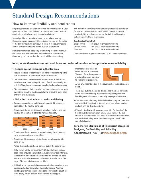
• Conductors should be staggered from layer to layer and not<br />
stacked on top of each other to increase flexibility.<br />
GOOD<br />
VS.<br />
BAD<br />
• Conductors should always be routed through bend areas as<br />
close to perpendicular as possible.<br />
• Incorporate tear stops or<br />
reliefs for slits in the circuit.<br />
The end of the slit represents<br />
a vulnerable point for a tear<br />
to start and to propagate.<br />
• Avoid any discontinuities in the cover coat or substrate near a<br />
bend.<br />
• The circuit outline should be designed so there are no twists<br />
in the finished assembly. Any burr or irregularity from the<br />
blanking operation could potentially propagate into a tear.<br />
• Consider factory forming. Reliable bend radii tighter than 10:1<br />
are possible if the circuit is formed using specialized tooling<br />
and will only be flexed one time.<br />
• If bend reliability is still a concern, consider "unbonding" the<br />
flexible substrates from each other. Since each of the substrates<br />
in the unbonded area has a much lower thickness than<br />
the total circuit, they are able to bend tighter than if they<br />
were fully bonded.<br />
For a more in-depth look at this subject please see<br />
Designing for Flexibility and Reliability<br />
Application Aid FAA31 - at www.minco.com/flex/<br />
• Conductor thickness and width should remain constant in<br />
bend areas.<br />
• Plated through holes should be kept out of the bend areas.<br />
• If the circuit will be bent within 1" (25.4mm) of termination<br />
pads, fillets should be placed at each conductor/pad interface.<br />
Stresses from a bend are not isolated to the immediate bend<br />
area and residual stresses can radiate out from the bend. See<br />
page 17 for more information on fillets.<br />
• If shields and/or ground planes are required on the circuit, use<br />
a crosshatched pattern rather than solid copper. Another<br />
shielding option is a screened-on conductive coating such as<br />
silver epoxy, which is much more flexible than copper.<br />
15