FLEX CIRCUITS DESIGN GUIDE
Minco Flex Circuits Design Guide - BiS Sistem
Minco Flex Circuits Design Guide - BiS Sistem
- No tags were found...

You also want an ePaper? Increase the reach of your titles
YUMPU automatically turns print PDFs into web optimized ePapers that Google loves.
Request a Quote<br />
Artwork checklist<br />
Minco strongly encourages customers to use the artwork<br />
checklist provided. If you answer 'yes' to all the criteria, your artwork<br />
will probably not need adjustment.<br />
Note: Depending on the size/complexity of the circuit, the criteria may<br />
differ.<br />
Dimensions<br />
• Does the border match the print dimensionally?<br />
• Does the artwork match the print dimensionally?<br />
Etched marking (if any)<br />
• Are all features of letters and symbols at least 0.010" (0.25mm)<br />
wide?<br />
• Are letters and symbols clear of conductors and borders?<br />
Border and cutouts<br />
• Is there a trim border (part outline) on at least one layer?<br />
• Do nominal borders allow for tolerances in the table on page 10?<br />
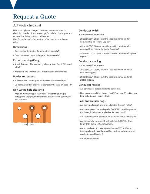
Non-wiring hole clearance<br />
• Are non-wiring holes at least 0.007" (0.18mm) (more preferred)<br />
over the specified minimum distance from conductors<br />
and borders?<br />
Conductor width<br />
Is artwork conductor width:<br />
• at least 0.001" (25μm) over the specified minimum for<br />
unplated 1/2 oz. (18μm) Copper?<br />
• at least 0.004" (100μm) over the specified minimum for<br />
unplated 1 oz. (35μm) (or thicker) copper?<br />
• at least 0.005" (125μm) over the specified minimum for plated<br />
copper?<br />
Conductor spacing<br />
Is artwork conductor space:<br />
• at least 0.001" (25μm) over the specified minimum for all<br />
unplated copper?<br />
• at least 0.002" (50μm) over the specified minimum for all<br />
plated copper?<br />
Conductor routing<br />
• Are conductors perpendicular to bend lines?<br />
• Have you avoided the I-beam effect? (See page 15 or Glossary<br />
for a definition of I-beam effect)<br />
Pads and annular rings<br />
• Are there pads on all layers for all plated through-holes?<br />
• Are non-exposed pads (via pads) 0.020" (0.51mm) larger than<br />
the through-holes (not applicable for micro vias)?<br />
• Are center locations provided for all drilled holes and/or slots?<br />
• Are the annular rings on all holes at .east 0.007" (0.18mm)<br />
larger than the specified minimum?<br />
• Are access holes in cover layers at least 0.007" (0.18mm)<br />
(more preferred) over the specified minimum distance from<br />
conductors and borders?<br />
• Are all pads filleted?<br />
25