FLEX CIRCUITS DESIGN GUIDE
Minco Flex Circuits Design Guide - BiS Sistem
Minco Flex Circuits Design Guide - BiS Sistem
- No tags were found...

You also want an ePaper? Increase the reach of your titles
YUMPU automatically turns print PDFs into web optimized ePapers that Google loves.
Request a Quote<br />
Designing CAD artworks<br />
This section provides the information necessary for designing<br />
CAD artworks that will meet the tolerance and quality requirements<br />
for a flex circuit. A correctly designed artwork will prevent<br />
unnecessary and costly delays in the initial shipment.<br />
Most CAD artwork is customer supplied. Minco can generate<br />
CAD artworks at additional cost. To generate an artwork, Minco<br />
needs:<br />
• Locations where the circuit will be bent, if any, and required<br />
flexibility at these locations (i.e. bending for installation or a<br />
dynamic application).<br />
• We prefer that you supply CAD generated data. If you cannot<br />
furnish CAD data, we can digitize a physical artwork at additional<br />
cost.<br />
• Outline dimensions and tolerances. See Page 18.<br />
• Location and size of conductor pads. See the table on page 16.<br />
• Minimum conductor widths, minimum spaces between conductors<br />
and conductor thickness. These will depend on current carrying<br />
capacity, impedance, dielectric, and the flexibility requirements<br />
of the circuit. See the nomograph on pages 12 – 13.<br />
• Net list<br />
• Conductor paths can be captured from a net list or schematic<br />
when required. A design charge may apply.<br />
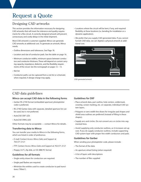
CAD-generated artwork<br />
CAD data guidelines<br />
Minco can accept CAD data in the following forms<br />
• Gerber RS-274X format (embedded aperture) photoplotter<br />
code is preferred.<br />
• RS-274D Gerber data with separate, detailed aperture list can<br />
be used, but is not preferred.<br />
• AutoCAD DXF (2D)<br />
• AutoCAD DWG (2D)<br />
Other formats may be acceptable — contact Minco for details.<br />
Transferring data to Minco<br />
You can transfer your media to Minco in the following forms,<br />
which are listed in order of preference.<br />
• E-mail: Contact Access: Minco Sales and Support at<br />
763.571.3121<br />
• FTP: Contact Access: Minco Sales and Support at 763.571.3121<br />
• Floppy (3.5"), Zip disk, or CD: IBM-PC format<br />
Guidelines for all formats<br />
• Single entity draws for conductors are required.<br />
Guidelines for DXF<br />
• Place artwork data, part outline, hole centers, soldermask,<br />
coverlay, screen marking, etc. on separate, individual CAD system<br />
layers.<br />
• Polygons or zero width line draws for irregular pad shapes and<br />
shield area outlines are preferred (instead of filling in these<br />
shapes).<br />
• Supply arcs and circles. Do not convert arcs or circles into segmented<br />
lines.<br />
• Avoid supplying only conductor outlines, as it increases set-up<br />
cost. If you do supply conductor outlines, include supporting<br />
CAD system layer with proper line width conductors and pads.<br />
Guidelines for Gerber<br />
When sending your photoplotter code, please include:<br />
• The format of the data<br />
• An aperture wheel listing (when required)<br />
• A list of layers with descriptions<br />
• The number of files supplied<br />
• Single pad flashes are required.<br />
• Minimize the entities used to create conductor to pad transitions<br />
(“fillets”).<br />
26